The estimation of impact ionization coefficients for -Ga2O3
Abstract
Impact ionization coefficients of anisotropic monoclinic -Ga2O3 are estimated along four crystallographic directions and the plot for the direction is shown. The approximation models were fitted to Baraff’s universal plot for ionization rate in semiconductors and the values were obtained for -Ga2O3. The phonon mean free path of -Ga2O3 was estimated to be 5.2604 using Gray medium approximation. The phonon group velocity takes the value of longitudinal acoustic phonons. The ionization rate has a maximum value of 3.98 106 along the direction over the applied electric field range (1.43-4) . Contrary to expectations, the phonon mean free path along direction is the lowest since it has a lower thermal conductivity to phonon group velocity ratio. The plots were compared with GaN and 4H-SiC, which shows that as bandgap increases the field required for ionization increases. The critical electric field was estimated to be 0.921 along direction.
I Introduction
The semiconductor industry dominated by Si-based technology has also explored various materials and compounds for specific-targeted applications. A wide variety of device designs Doering and Nishi (2007); O’Mara et al. (2007) have been studied for applications as diverse as high-power switching Shenai et al. (1989) to opto-electronic control Denbaars (1997); Sengupta et al. (2011) of physical processes. However, there is still a need for improved material sets, for instance, silicon carbide (SiC) and wurtzite gallium nitride (GaN) are now well-established as foundational blocks for power electronic components. These compound semiconductors possess desired power electronics specific material properties, for example, a large band gap and high breakdown field . A substantial body of work focussed on SiC and GaN power devices is available, however, there still lies areas where improved performance is desired. Recently, monoclinic Ga2O3 by virtue of its extraordinary material properties, an impressive Baliga’s figure of merit (larger than those of Si, SiC and GaN) has renewed interest in applications centred around power switching, RF amplifiers, and in general signal processing under high electric field operational conditions. Its manifold uniqueness therefore warrants more accurate study of material physics, related device technologies, and an overall better understanding of its core set of physical properties. The intrinsic set of advantages notwithstanding and coupled to previous acquaintance with this material when they were bulk melt-grown as substrates, their commercial viability remains poor vis-à-vis silicon and their derivatives currently in use. A particularly attractive way of probing a material deeper lies in the use of simulation tools that offset the cost of expensive experimental efforts. TCAD Simulation tools Fonseca et al. (2013) help in reducing the cost while improving the quality of experimental research by highlighting device structures with desired output characteristics, but the majority of the tools and methods are oriented towards silicon based devices. While methods, models and coefficients, semi-empirical band-structure calculation techniques Klimeck et al. (2000); Sengupta et al. (2016) are available for other materials like SiC, GaN and InP, little to no data are available for Ga2O3. In this work we will determine such coefficients and desirable models to be used for -Ga2O3, particularly the coefficients for impact ionization modelling since the major focus on -Ga2O3 is for power applications.
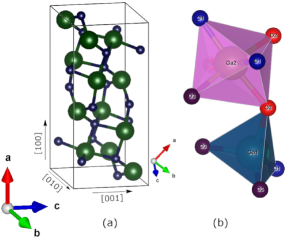
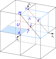
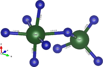
Gallium Oxide single crystals exhibit polymorphism Roy et al. (1952) with five confirmed polytypes , of which the anisotropic monoclinic -Ga2O3 is the most stable polymorph, thermodynamically. The unit cell of -Ga2O3, shown in Fig 1, consists of two inequivalent Ga sites (large spheres), three inequivalent O-sites (small spheres) and contains a total of 30 atoms and the primitive cell comprises 10 atoms. The tetrahedral and octahedral geometry of Ga1 and Ga2 sites are illustrated in Fig 1. A detailed geometry as given in Ref. Åhman et al., 1996; Geller, 1960 is illustrated in Appendix A. The lattice parameters corresponding to the crystallographic axis of -Ga2O3 unit cell are given as, a = 12.214 , b = 3.037 , c = 5.7981, and = 103.83 (between a and c) (Åhman et al., 1996), which implies that this crystal belongs to the C12/m1 space group for which the parallelpiped reciprocal lattice vector unit cell Brillouin zone schematic is shown in Fig 2, Bradley and Cracknell (2010); Aroyo et al. (2006a, b, 2011, 2014) and a detailed Brillouin zone computed using the primitive cell was suggested by H. Peelaers and C. G. Van de Walle Peelaers and Van de Walle (2015).
The dielectric constant of -Ga2O3 was set to 10.2, as given in Refs. Passlack et al., 1994; Hoeneisen et al., 1971, and the experimentally obtained band gap is ultra wide Janowitz et al. (2011); Tippins (1965); Matsumoto et al. (1974); Orita et al. (2000) at 4.85 0.1 eV and has an experimental electrical breakdown field of 3.6 Passlack et al. (1995) though the theoretical limit was estimated to be 8 , Hudgins et al. (2003) which encourages researchers towards the development of Ga2O3 devices, specifically for its applications in power electronics. Experimental estimates measure the effective electron mass to be around 0.3 Binet et al. (1994) and combining this with the first principle calculations a good compromise for will be 0.28, Varley et al. (2010); Yamaguchi (2004); He et al. (2006a) from which the conduction band density of states is be calculated as Nc= 3.71018 . Irmscher et al. (2011) The polymorph of Ga2O3 has been studied extensively over other polytypes owing to its thermal and chemical stability and ease of substrate preparation from melt based growth techniques, and the thermal conductivity measured to be 27 2.0, 14.71.5, 13.31.0 and 10.9 1.0 W/m-K for crystallographic directions , , and respectively, Guo et al. (2015) is different along different crystallographic axis, due to the crystal’s anisotropic nature.
Due to the lack of fundamental research, the estimation of impact ionization coefficients, namely ionization rate (), critical electric field (), applied electric field () and ionization rate constant (), depends on the determination of phonon mean free path and fortunately enough data is available to estimate this value. Phonon mean free path was calculated to be 5.2604, 3.0675, 2.99 and 2.736 , for crystallographic directions , , and , respectively. The impact ionization rates were calculated using the standard impact ionization models provided by Crowell-Sze, Sutherland and Thornber and these values were used in Selberherr IIM. The model suggested by Sutherland in Ref. Sutherland, 1980 provides the best fit to Universal Baraff’s Curve for ionization rates, and has the values 3.98 106, 7.626 106, 8.965 106 and 9.485 106 cm -1 for crystallographic directions , , and .
II Methods and Models
Several impact ionization models can be used for the estimation of ionization rate, which consecutively aids in determining the breakdown voltage. Selberherr’s model Siegfried (1984), which is a modification of Chynoweth’s law, takes the following expression,
| (1) |
where, is the ionization rate, the impact ionization rate constant, is the critical electric field, is the applied electric field strength at a specific position in the direction of current flow, and , a fitting constant, is in the range 1 to 2. The ionization coefficients for holes take similar values to that of electrons, for the purpose of simulations. To estimate the coefficients for Selberherr’s model, the numerical approximation methods provided by Crowell-Sze, Sutherland and Thornber are fitted to Baraff’s universal plot Baraff (1962) for ionization rate in semiconductors. Baraff plot follows the relation,
| (2) |
where, is the ionization rate, the phonon mean free path, the optical phonon energy, the ionization energy.
The Baraff curve approximation proposed by Crowell and Sze Crowell and Sze (1966) is expressed as,
| (3a) | ||||
| with: | ||||
| (3b) | ||||
| (3c) | ||||
| (3d) | ||||
| where, | ||||
| (3e) | ||||
| (3f) | ||||
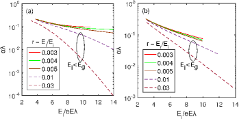
This approximation is accurate over the range r and x within two percent maximum error. A more rigorous approximation was proposed by Sutherland Sutherland (1980) given by,
| (4a) | |||
| with: | |||
| (4b) | |||
| (4c) | |||
| (4d) | |||
| (4e) | |||
For the range r and x this approximation is expected to fit Baraff’s curve perfectly. The empirical expression proposed by Thornber Thornber (1981) has been consistent with an elaborate momentum and energy scaling theory and is given by,
| (5a) | ||||
| where, | ||||
| (5b) | ||||
| (5c) | ||||
is the threshold field at which the ionization energy is reached in one mean free path and is when phonon energy is reached in one mean free path. To determine the value of impact ionization rates from the above expressions, we need to determine the value of optical phonon mean free path (MFP), on which not much experimental or theoretical research has been done and no data is available for -Ga2O3. The value of MFP can be determined from its relation to thermal conductivity and specific heat capacity provided as Gray’s approximation,
| (6) |
where is the thermal conductivity, is the phonon group velocity (values for is available in Ref Guo et al., 2015), is the phonon mean free path, which needs to be determined, is the specific heat capacity which is calculated using the Debye model of specific heat represented as,
| (7) |
where, and is the Debye temperature, which can take the experimentally measured value of 738 K Guo et al. (2015) or the first principles estimate of 872 K He et al. (2006b) for -Ga2O3, is the absolute temperature, is the Boltzmann constant and is the number of atoms, considered as Avogadro’s number. We considered the experimentally measured value for Debye temperature.
The models described above are pseudolocal in nature. Hence, the ionization rates calculated depend only on the electric field strength applied but not on the position where the carriers are generated. This suggests that the models can be used for any position within the space-charge region, which is not true. Such a description assumes an unphysical situation within the device for structures with sufficiently high multiplication. A critical multiplication ratio , between the ionized and the total number of carriers at a any position in the structure, was suggested by Okuto and Crowell in Ref. Okuto and Crowell, 1974 to address this pseudolocal issue in their non-localized concept description of avalanche ionization effect. Mc is given by the following relation,
| (8a) | ||||
| with: | ||||
| (8b) | ||||
| (8c) | ||||
| (8d) | ||||
| (8e) | ||||
where is the net number of optical phonons absorbed by the carrier and is assumed as zero, since only absorption of energy is considered at low temperatures. X, is the average distance at which an ionizatoin scattering occurs, D, is the dark-space distance, is the non-localized single-carrier ionization probability, is the “apparent ionization coefficient” introduced in Ref Okuto and Crowell, 1974. The expression for has the following theoretical limits,
| (9a) |
| (9b) |
III Results
In order to estimate the impact ionization coefficients we first determine the value for optical phonon mean free path () using Eq. 6 where the values used for thermal conductivity, phonon group velocity and specific heat capacity are listed in Table 1. Owing to anisotropy in the crystal structure, the approximate values of are obtained for different crystallographic directions as catalogued in Table II. These estimates are justified when we compare the thermal conductivities of -Ga2O3 and GaN given as 27 and 230 W/m-K Jeżowski et al. (2003), respectively. The phonon group velocity and specific heat capacity of GaN is determined to be 6.9-8.2 , Truell et al. (2013) and 0.49 °, Levinshtein et al. (2001) respectively. Corresponding values for -Ga2O3 are 7.8 and 0.56 ° (for direction) Galazka et al. (2014). The difference is 5% for phonon group velocity and 13% for specific heat capacity between the two compound semiconductors. Using Eq. (6) we see that the phonon mean free path is the only variable affecting thermal conductivity and has to be larger in GaN than -Ga2O3. In fact of GaN is larger by an order of 10 from Ref Danilchenko et al., 2006. We should note that the thus obtained is for the acoustic branch. We consider a situation where no acoustic phonons are present. If the energy of the electron is below the optical phonon energy the mean free path will be infinite since no collision will take place unless the electron gains energy above the optical phonon energy. The presence of acoustic phonons gives a maximum value for beyond which it cannot increase, and this estimation will be a good approximation for the purpose of calculating the ionization coefficients. The value of is estimated to be 5.2604 for -Ga2O3 along the direction, and takes the value 24.81 meV from Ref. Kranert et al., 2016.
| Crystallographic direction | Thermal Conductivity | Phonon group velocity |
| 27 2.0 | 7.8 | |
| 10.91.5 | 5.4 | |
| 14.71.0 | 7.1 | |
| 13.31.0 | 6.6 |
| Crystallo graphic direction (Material) | Impact ionization rate () [] | Critical Electric Field () [] | Phonon Mean Free Path ()[] | Applied Electric Field[ ] |
| 3.98 | 0.921 | 5.260 | 1.43-4 | |
| 7.626 | 1.581 | 3.067 | 3.37-7.7 | |
| 8.965 | 1.622 | 2.99 | 3.08-9.2 | |
| 9.485 | 1.755 | 2.763 | 3.5-9.7 | |
| (GaN) | 0.25 | 0.34 | 580 | 0.12-0.53 |
| (4H-SiC) | 0.15 | 0.16 | 32.5 | 0.09-0.35 |
Baraff adopts an approach which neither relies on diffusion approximation followed by Wolff wolff1954theory nor Shockley’s shockley1961problems “spike” distribution to describe electron transport but rather derives an integral equation for the collision density in order to estimate ionization rates, for all semiconductors. The curves from the mathematical models discussed in section II must fit this universal plot provided by Baraff for different values of ionization energy () over the range of applied electric field strength . The values to which they fit for -Ga2O3 are given in Table 2. The Baraff plots illustrated are for Sutherland model, Fig.3, and Thornber model, Fig.3, from which we can observe that Sutherland model fits more perfectly and for a larger range than Thornber model. Thus the values of ionization rate and applied electric field strength are calculated using Sutherland model. The solid lines are for values where the ionization energy is above the bandgap energy and the dashed lines are for values of below . The probability of ionization is less for values of below , but are shown to clarify that the approximation models fit the Baraff curve. The range in which the values for ionization rate, , and applied electric field strength are reliable for the material under consideration can also be extracted from Baraff curve. The plot for the model provided by Crowell-Sze is not shown. The figures are plotted only for , since the thermal conductivity is maximum along this direction. The estimates of the coefficients and are extracted from Fig. 4 (ionization coefficient inverse electric field) and Fig. 4 (log-log plot) respectively. The ionization rate constant, , can be calculated from these values using Eq. (1). The values of , and used to plot Fig. 4 are 5.2604, 24.81 meV and 7.275 eV (i.e., 1.5 ), respectively. There are no experimental verification available for ionization rates of -Ga2O3.
The ionization rate constant can be estimated from its relationship to ionization rate, critical field and applied field as shown in Eq. (1). The range of values thus obtained are for a range of the electric field estimated from Baraff plot. The exact value of ionization rate constant, , can only be determined through experimentation, or at the least by knowing the breakdown voltage and related electric field applied to the device under consideration. We predict the ionization rate constant to be ( 2.51 109 - 3.9 107) cm-1 over the applied electric field range of ( 1.43 107 - 4 107) V cm-1. The predicted values for ionization coefficients are listed in Table. 2 and given the large energy band gap of -Ga2O3, the value estimated for applied electric field strength can be justified when juxtaposed with other wide-bandgap semiconductors.
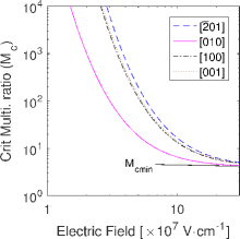
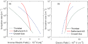
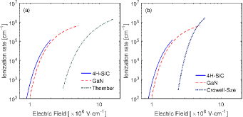
A comparison of plots between major wide-bandgap semiconductor materials considered for power electronics can be derived from Fig. 5. The curves were traced using the variables described in section II with parameters from Ref. Danilchenko et al., 2006; Jeżowski et al., 2003; Levinshtein et al., 2001; ouguzman1997theory; Truell et al., 2013 for GaN, Ref. choyke1969optical; berger1996semiconductor; harris1995properties; konstantinov1997ionization for 4H-SiC. The applied field strength range at which ionization occurs is larger in -Ga2O3 than GaN or 4H-SiC and a similar comparison can be made for materials germanium, silicon, gallium arsenide and gallium phosphide from Ref. okuto1972energy. The increase in applied field is attributed to the bandgap of the material since the field strength required for ionization increases as the bandgap increases. The ionization rate depends on the values of phonon mean free path and optical phonon energy . The phonon mean free path determines, the average distance a carrier has to travel to acquire enough energy for ionization and influences the ratio of “cross section” () for ionization. Comparing and of gallium oxide to corresponding values of GaN and 4H-SiC predicts the ionization rate to be higher in -Ga2O3, as estimated. The critical multiplication ratio discussed in section II aids in understanding the limitations of the ionization models and the numerically calculated is shown in Fig. 6. If the ratio of the total number carriers to the ionized carrier is higher than then the models do not hold and if it is lower the boundary conditions are important. We can see that has a large value at low field and saturates at high field as predicted by the theoretical limits and also notice that the field strength at which the multiplication holds is high and compliments the field strength obtained from Baraff plots.
IV Conclusion
We have estimated the ionization coefficients of -Ga2O3 using approximation models provided by Crowell-Sze, Thornber and Sutherland, for Baraff’s universal plot of ionization rates in semiconductors. The phonon mean free path was estimated using Gray approximation of thermal conductivity and debye’s model was used to determine specific heat. The ionization rate curves thus determined were compared with other major power semiconductors (GaN and 4H-SiC), and it was found that as the bandgap increases the field strength required for ionization also increases, regardless of phonon energy. Values for critical multiplication ratio of the carriers was determined to address the pseudolocal nature of the approximations. A plot for the same is illustrated and above these values the models do not hold.
The ionization rate constant can be determined by measuring the breakdown voltage and the electric field at this breakdown. Using the measured applied field, in the expression for ionization rate, we can deduce the ionization rate constant. Alternatively, existing breakdown values of gallium oxide devices can be used, provided we know the crystal orientation of the channel of the device during breakdown. Then this device can be simulated for the suggested range of values of ionization rate until the measured breakdown voltage is obtained. Finally, the ionization rate constant can be calculated using its relation to ionization rate and applied electric field.
The approximation models considered in this work, although developed based on silicon and gallium arsenide, holds true for a wide bandgap semiconductor, such as gallium oxide, since the carrier density approach by Baraff is universal for all semiconductors. The dependence of ionization rate to the change in carrier concentration was not considered. An experimental analysis measuring Id-Vd characteristics of -Ga2O3 MOSFET, such as in Ref. higashiwaki2013depletion and recording information on breakdown voltage and applied electric field, will assist in verifying the estimated ionization coefficient values.
Appendix A Geometry of -Ga2O3
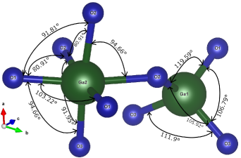
The bond lengths and angles for the two Ga sites are given in Table 4 and 5 and illustrated in Fig. 7 and 8.
| Element | x | y | z | |
|---|---|---|---|---|
| Ga1 | 0.09050(2) | 0 | 0.7946(5) | 0.0038(1) |
| Ga2 | 0.15866(2) | 0.31402(5) | 0.0040(1) | |
| O1 | 0.1645(2) | 0 | 0.1098(3) | 0.0060 (4) |
| O2 | 0.1733(2) | 0 | 0.5632(4) | 0.0056 (4) |
| O3 | 0.2566(3) | 0.0042(4) |
| Bonds | Bond length () |
|---|---|
| Gal–O1i | 1.835(2) |
| Ga1–O2 | 1.863(2) |
| Gal–O3ii | 1.833(1) |
| Ga2–O1 | 1.937(1) |
| Ga2–O2 | 2.074(1) |
| Ga2–O2iii | 2.005(2) |
| Ga2–O2 | 1.935(2) |
The equivalent isotropic displacement parameter, , is given by,
| (10) |
| Bonds | Angles() |
|---|---|
| O1i–Gal–O2 | 119.59(9) |
| O1i–Gal–O3ii | 106.79(7) |
| O2i–Ga1–O3ii | 105.92(7) |
| O3ii–Gal–O3iv | 111.9(1) |
| O1i–Ga2–O1v | 103.22(9) |
| O1–Ga2–O2 | 80.91(6) |
| O1i–Ga–O2iii | 91.87(7) |
| O1–Ga2–O3 | 94.66(7) |
| O2–Ga2–O2v | 94.14(7) |
| O2–Ga2–O2iii | 80.91(6) |
| O2–Ga2–O3 | 91.95(7) |
(i) x,y,1+z; (ii) -x,-y,1-z; (iii) -x,-y,1-z; (iv) -x,1-y,1-z; (v) x,1+y,z.
References
- Doering and Nishi (2007) R. Doering and Y. Nishi, Handbook of semiconductor manufacturing technology (CRC Press, 2007).
- O’Mara et al. (2007) W. O’Mara, R. B. Herring, and L. P. Hunt, Handbook of semiconductor silicon technology (Crest Publishing House, 2007).
- Shenai et al. (1989) K. Shenai, R. S. Scott, and B. J. Baliga, IEEE transactions on Electron Devices 36, 1811 (1989).
- Denbaars (1997) S. Denbaars, Proceedings of the IEEE 85, 1740 (1997).
- Sengupta et al. (2011) P. Sengupta, S. Lee, S. Steiger, H. Ryu, and G. Klimeck, MRS Online Proceedings Library Archive 1370 (2011).
- Fonseca et al. (2013) J. E. Fonseca, T. Kubis, M. Povolotskyi, B. Novakovic, A. Ajoy, G. Hegde, H. Ilatikhameneh, Z. Jiang, P. Sengupta, Y. Tan, et al., Journal of Computational Electronics 12, 592 (2013).
- Klimeck et al. (2000) G. Klimeck, R. C. Bowen, T. B. Boykin, C. Salazar-Lazaro, T. A. Cwik, and A. Stoica, Superlattices and Microstructures 27, 77 (2000).
- Sengupta et al. (2016) P. Sengupta, H. Ryu, S. Lee, Y. Tan, and G. Klimeck, Journal of Computational Electronics 15, 115 (2016).
- Geller (1960) S. Geller, The Journal of Chemical Physics 33, 676 (1960).
- Åhman et al. (1996) J. Åhman, G. Svensson, and J. Albertsson, Acta Crystallographica Section C: Crystal Structure Communications 52, 1336 (1996).
- Roy et al. (1952) R. Roy, V. Hill, and E. Osborn, Journal of the American Chemical Society 74, 719 (1952).
- Bradley and Cracknell (2010) C. Bradley and A. Cracknell, The mathematical theory of symmetry in solids: representation theory for point groups and space groups (Oxford University Press, 2010).
- Aroyo et al. (2006a) M. I. Aroyo, A. Kirov, C. Capillas, J. Perez-Mato, and H. Wondratschek, Acta Crystallographica Section A: Foundations of Crystallography 62, 115 (2006a).
- Aroyo et al. (2006b) M. I. Aroyo, J. M. Perez-Mato, C. Capillas, E. Kroumova, S. Ivantchev, G. Madariaga, A. Kirov, and H. Wondratschek, Zeitschrift für Kristallographie-Crystalline Materials 221, 15 (2006b).
- Aroyo et al. (2011) M. I. Aroyo, J. Perez-Mato, D. Orobengoa, E. Tasci, G. De La Flor, and A. Kirov, Bulg. Chem. Commun 43, 183 (2011).
- Aroyo et al. (2014) M. I. Aroyo, D. Orobengoa, G. de la Flor, E. S. Tasci, J. M. Perez-Mato, and H. Wondratschek, Acta Crystallographica Section A: Foundations and Advances 70, 126 (2014).
- Peelaers and Van de Walle (2015) H. Peelaers and C. G. Van de Walle, physica status solidi (b) 252, 828 (2015).
- Passlack et al. (1994) M. Passlack, N. Hunt, E. Schubert, G. Zydzik, M. Hong, J. Mannaerts, R. Opila, and R. Fischer, Applied physics letters 64, 2715 (1994).
- Hoeneisen et al. (1971) B. Hoeneisen, C. Mead, and M. Nicolet, Solid-State Electronics 14, 1057 (1971).
- Janowitz et al. (2011) C. Janowitz, V. Scherer, M. Mohamed, A. Krapf, H. Dwelk, R. Manzke, Z. Galazka, R. Uecker, K. Irmscher, R. Fornari, et al., New Journal of Physics 13, 085014 (2011).
- Tippins (1965) H. Tippins, Physical Review 140, A316 (1965).
- Matsumoto et al. (1974) T. Matsumoto, M. Aoki, A. Kinoshita, and T. Aono, Japanese journal of applied physics 13, 1578 (1974).
- Orita et al. (2000) M. Orita, H. Ohta, M. Hirano, and H. Hosono, Applied Physics Letters 77, 4166 (2000).
- Passlack et al. (1995) M. Passlack, E. Schubert, W. Hobson, M. Hong, N. Moriya, S. Chu, K. Konstadinidis, J. Mannaerts, M. Schnoes, and G. Zydzik, Journal of applied physics 77, 686 (1995).
- Hudgins et al. (2003) J. L. Hudgins, G. S. Simin, E. Santi, and M. A. Khan, IEEE Transactions on Power Electronics 18, 907 (2003).
- Binet et al. (1994) L. Binet, D. Gourier, and C. Minot, Journal of Solid State Chemistry 113, 420 (1994).
- Varley et al. (2010) J. Varley, J. Weber, A. Janotti, and C. Van de Walle, Applied Physics Letters 97, 142106 (2010).
- Yamaguchi (2004) K. Yamaguchi, Solid state communications 131, 739 (2004).
- He et al. (2006a) H. He, R. Orlando, M. A. Blanco, R. Pandey, E. Amzallag, I. Baraille, and M. Rérat, Physical Review B 74, 195123 (2006a).
- Irmscher et al. (2011) K. Irmscher, Z. Galazka, M. Pietsch, R. Uecker, and R. Fornari, Journal of Applied Physics 110, 063720 (2011).
- Guo et al. (2015) Z. Guo, A. Verma, X. Wu, F. Sun, A. Hickman, T. Masui, A. Kuramata, M. Higashiwaki, D. Jena, and T. Luo, Applied Physics Letters 106, 111909 (2015).
- Sutherland (1980) A. Sutherland, IEEE Transactions on Electron Devices 27, 1299 (1980).
- Siegfried (1984) S. Siegfried, Analysis and simulation of semiconductor devices (1984).
- Baraff (1962) G. A. Baraff, Physical review 128, 2507 (1962).
- Crowell and Sze (1966) C. Crowell and S. Sze, Applied Physics Letters 9, 242 (1966).
- Thornber (1981) K. Thornber, Journal of Applied Physics 52, 279 (1981).
- He et al. (2006b) H. He, M. A. Blanco, and R. Pandey, Applied physics letters 88, 261904 (2006b).
- Okuto and Crowell (1974) Y. Okuto and C. Crowell, Physical Review B 10, 4284 (1974).
- Jeżowski et al. (2003) A. Jeżowski, B. Danilchenko, M. Boćkowski, I. Grzegory, S. Krukowski, T. Suski, and T. Paszkiewicz, Solid state communications 128, 69 (2003).
- Truell et al. (2013) R. Truell, C. Elbaum, and B. B. Chick, Ultrasonic methods in solid state physics (Academic press, 2013).
- Levinshtein et al. (2001) M. E. Levinshtein, S. L. Rumyantsev, and M. S. Shur, Properties of Advanced Semiconductor Materials: GaN, AIN, InN, BN, SiC, SiGe (John Wiley & Sons, 2001).
- Galazka et al. (2014) Z. Galazka, K. Irmscher, R. Uecker, R. Bertram, M. Pietsch, A. Kwasniewski, M. Naumann, T. Schulz, R. Schewski, D. Klimm, et al., Journal of Crystal Growth 404, 184 (2014).
- Danilchenko et al. (2006) B. Danilchenko, T. Paszkiewicz, S. Wolski, A. Jeżowski, and T. Plackowski, Applied physics letters 89, 061901 (2006).
- Kranert et al. (2016) C. Kranert, C. Sturm, R. Schmidt-Grund, and M. Grundmann, Scientific Reports 6, 35964 (2016).