Disrupted orbital order and the pseudo-gap in layered 1T-TaS2
Abstract
We present a state-of-the-art density functional theory (DFT) study which models crucial features of the partially disordered orbital order stacking in the prototypical layered transition metal dichalcogenide 1T-TaS2. Our results not only show that DFT models with realistic assumptions about the orbital order perpendicular to the layers yield band structures which agree remarkably well with experiments. They also demonstrate that DFT correctly predicts the formation of an excitation pseudo-gap which is commonly attributed to Mott-Hubbard type electron-electron correlations. These results highlight the importance of interlayer interactions in layered transition metal dichalcogenides and serve as an intriguing example of how disorder within an electronic crystal can give rise to pseudo-gap features.
The spontaneous formation of so-called electronic crystals, i.e., spatial superlattices formed collectively by the valence electrons of a solid is among the most striking topics in current condensed matter research Monceau (2012); Grüner (1994). Charge density wave (CDW) order is a manifestation of such macroscopic collective quantum states which occurs in a wide range of materials, including doped copper oxide systems Chaix et al. (2017); Chang et al. (2012), heavy fermion systems Gruner et al. (2017) or layered transition metal dichalcogenides (TMDs) Wilson et al. (1975). In particular the latter class of materials currently regains enormous attention as “post graphene” quasi two-dimensional materials. Their unusual electronic properties propel innovative concepts for applications ranging from miniaturized electronic devices to quantum computing Stojchevska et al. (2014); Yoshida et al. (2015); Vaskivskyi et al. (2016); Ma et al. (2016); Pan et al. (2017).
Owing to the weak bonding between the layers, the TMDs are traditionally considered to realize rather two-dimensional electronic systems. However, recent theoretical and experimental work suggests that, due to orbital order which is intertwined with the CDW, the electronic structure markedly depends on the stacking arrangement of this combined order in the direction perpendicular to the layers Ge and Liu (2010, 2012); Darancet et al. (2014); Ritschel et al. (2015); Chen et al. (2016); Navarro-Moratalla et al. (2016); Hovden et al. (2016); Dolui and Sanvito (2016). Accordingly, density functional theory (DFT) based on oversimplified assumptions about the CDW stacking will yield electronic structures that do not agree with experiment Ritschel et al. (2015). In this letter we present a DFT model that realistically approximates the experimentally found partially disordered CDW stacking for the prototypical material 1T-TaS2 and compare these calculations to angle resolved photoemission spectroscopy data. 1T-TaS2 serves here as a prime example to study the effect of disorder within the orbital sector on the electronic structure.
Among the TMDs 1T-TaS2 is well known for its particularly rich electronic phase diagram as a function of temperature and pressure Sipos et al. (2008). Starting at ambient pressure and low temperatures the in-plane (IP) CDW order is commensurate (C) with the underlying crystal lattice. It is characterized by star-of-david shaped clusters comprising 13 Tantalum sites arranged in a IP superstructure as illustrated in Fig. 1 (a). Increasing the temperature or rising the external pressure yields a so-called nearly commensurate (NC)-CDW which is associated with the creation of defects within the C-CDW which, by themselves, order on an again larger length scale Spijkerman et al. (1997). At higher temperatures or pressures the NC-CDW transforms into incommensurate (IC)-CDWs.
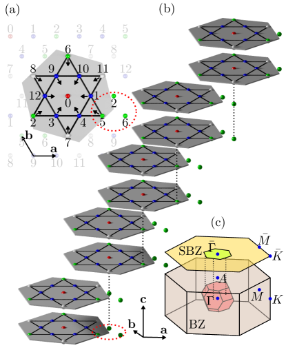
Interestingly, not only the IP structure is effected by the transitions between the different CDWs but also the stacking arrangement in the out-of-plane (OP) direction. The IC-CDW and the NC-CDW possess a well ordered stacking along the OP direction with a periodicity corresponding to three times the layer-to-layer distance Å Spijkerman et al. (1997). In contrast, the C-CDW is governed by a complex alternating and partially disordered stacking along the OP direction: According to the 13 Tantalum sites forming one star-of-david cluster (labels in Fig. 1 (a)), there are 13 possibilities of how two adjacent layers are aligned with respect to each other. We introduce the following notation: An arrangement where the central site, i.e. site 0, within a star-of-David cluster is centered above site in the layer below is referred to as . Taking the threefold IP symmetry of the C-CDW into account the 13 distinct stacking types form 5 symmetry equivalent groups, namely , , , and . Although the stacking of the C-CDW in 1T-TaS2 is still debated, there is firm theoretical Walker and Withers (1983); Nakanishi and Shiba (1984) and experimental Tanda et al. (1984); Ritschel et al. (2015) evidence that it can be viewed as bilayers which are stacked on top, i.e., stacking . These bilayers, for their part, are stacked by a random choice out of the three symmetry equivalent possibilities corresponding to the group . The resulting alternating partially disordered stacking, which we will denote by is illustrated in Fig. 1 (b). To the best of our knowledge, the peculiar disordered C-CDW stacking is only found in 1T-TaS2. The closely related material 1T-TaSe2 develops the same IP C-CDW structure. However, in this material the stacking is governed by the formation of macroscopic domains with a long-range ordered stacking corresponding to one stacking out of the group Wiegers et al. (2001). Interestingly, it has been shown, that this long-range OP stacking order can be transformed into a disordered stacking among the group by subtle doping of Zr impurities on the Ta site Moncton et al. (1976). However, as opposed to 1T-TaS2 there is no alternation between different stacking groups.
Another remarkable feature of the C-CDW in 1T-TaS2 lies in its semiconducting transport properties. Commonly, this is attributed to Mott-Hubbard type electron-electron correlations. According to this scenario every star-of-David cluster contributes a single 5d electron to a half filled narrow conduction band. A sufficiently large Coulomb repulsion acting on these clusters is believed to drive a Mott-Hubbard transition with overlapping Hubbard subbands Fazekas and Tosatti (1979, 1980). It has been proposed that Anderson localization finally drives a metal-to-insulator transition at low temperatures yielding the observed semiconducting transport properties Dardel et al. (1992a, b). It should be noted that a semiconducting CDW phase is very uncommon among the class of TMDs. All other CDW phases are metallic or even superconducting at low temperatures Rossnagel (2011). Recently, time and angle resolved photoemission spectroscopy (trARPES) was employed to observe the ultrafast collapse of an excitation gap at the Brillouin zone center (-point, cf. Fig. 1 (c)) – the so called Mott gap – which was interpreted as a clear signature that electronic degrees of freedom are involved in the formation of this gap Perfetti et al. (2008); Hellmann et al. (2010, 2012).
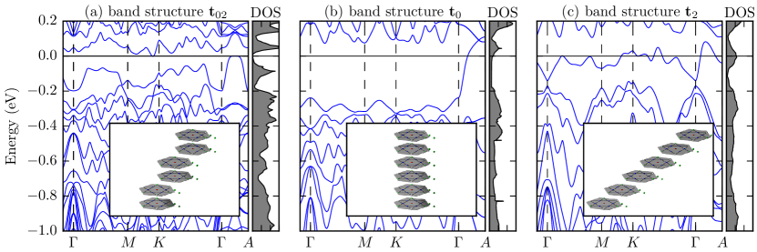
However, in what follows we will use an extension of our previous DFT approach Ritschel et al. (2015) to show that the transport properties and in particular the gap at of the C-CDW phase can be inferred from the actual CDW stacking. All DFT calculations have been done using the FPLO14 package Koepernik and Eschrig (1999). Following our previous approach the IP supercell structure was derived from reference Brouwer, 1978 and Spijkerman et al., 1997. In order to incorporate the different stacking types we constructed triclinic supercells without changing the atomic displacements and using the experimental interlayer distance Brouwer (1978). The disordered alternating stacking of the C-CDW as illustrated in Fig. 1 (b) does not obey translational symmetry in the OP direction and, hence, it cannot be treated in a conventional DFT bandstructure scheme. In order to circumvent this difficulty we approximate the disordered stacking by a periodic alternation of the stacking and . In other words, the partial disorder among the group of symmetry equivalent stacking types is neglected and a single fixed stacking is chosen. We denote this stacking, which is visualized in the inset of Fig. 2 (a), by . In Fig. 2 (a) we show the result of a DFT bandstructure calculation for this periodically alternating stacking. For comparison we also reproduce the bandstructure calculations from Ref. Ritschel et al., 2015 for the non-alternating stacking types and in Fig. 2 (b) and (c), respectively.
The first and most important observation is that the DFT calculation within the local density approximation (LDA) which takes the alternating stacking into account indeed yields a gap-like feature at the Fermi energy. This can be most clearly seen from the density of states (DOS) shown in the right panel of Fig. 2 (a). Thus, the key result of these calculations is that LDA predicts an insulating or semiconducting ground state for the alternating stacking . In contrast, the non-alternating stacking types and possess a Fermi surface and, hence, our LDA calculations predict metallic ground states (cf. Fig. 2 (b) and (c)) in accordance with previous calculations Bovet et al. (2003); Ge and Liu (2010); Darancet et al. (2014); Ritschel et al. (2015).
Although the formation of this gap is surprising at first glance it can be understood in terms of elementary band theory arguments: The supercell corresponding to stacking or contains an odd number of electrons (13 Tantalum sites each contributing one 5d electron). LDA calculations for these stacking types result in metallic ground states as the valence band is partially filled. In order to model the alternating stacking it is necessary to include two star-of-David clusters in the supercell. Accordingly, the resulting even number of electrons in this supercell can yield a completely filled valence band and thus an insulating or semiconducting ground state. However, this line of arguments does certainly not allow to deduce the size of the gap. Depending on subtle details of the hopping integrals between wavefunctions in adjacent layers the gap size could indeed be zero or there could even be a small overlap of valance and conduction band resulting in a semimetal with conducting behavior at finite temperatures. Interestingly, the band structure and DOS shown in Fig. 2 (a) suggest exactly such a zero-gap semiconductor for the case of the -stacking. Measurements of the Hall effect in 1T-TaS2 find semiconducting or semimetallic behavior in the C-CDW phase of 1T-TaS2, which supports our theoretical result Inada et al. (1980).
We will now assess the validity of our LDA model of the C-CDW phase by a detailed comparison of the calculated electronic band structure to angle-resolved photoemission spectroscopy (ARPES) measurements. To this end we have measured the valance electronic structure of a high quality single crystal of 1T-TaS2 as a function of and which, together with the energy-axis, yields a 3D data set. These measurements were performed at the -ARPES endstation at beamline UE112PG2 of the Berlin Synchrotron (BESSY). We used -polarized light of 96 eV photon energy, so that the final state crystal momentum at normal emission corresponds to the -point Rossnagel et al. (2005). The sample temperature was kept at 1 K. In Fig. 3 we compare various cuts through the obtained 3D data set with corresponding DFT calculations.
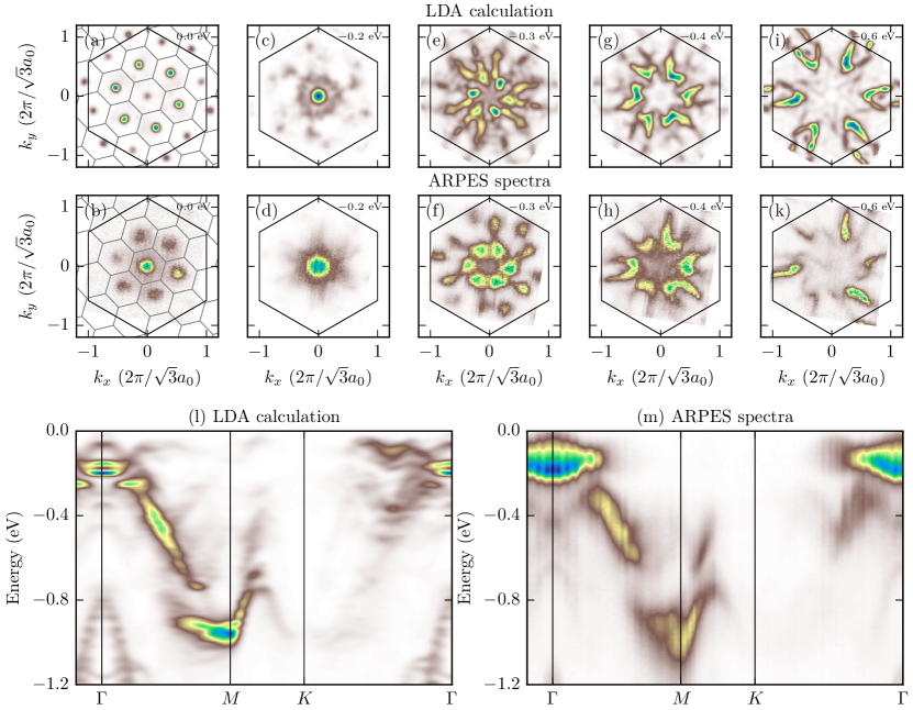
We use the unfolding scheme which is described in Ref. Ku et al., 2010. This approach facilitates a comparison of the theoretical bandstructures to the experimentally accessible spectral function Damascelli et al. (2003). Furthermore we use a heuristic approximation in order to mimic the effect of the partial disorder which is a marked characteristic of the CDW stacking in 1T-TaS2: Since the three vectors , and occur randomly in the partially disordered stacking the whole structure obeys, on average, threefold rotational symmetry. This symmetry is broken by the approximation , where only occurs. For a comparison to ARPES data we have therefore symmetrized the calculated unfolded bandstructure for in order to restore the threefold symmetry. This symmetrization bears on the assumption that, on average, the effect of the disorder on the electronic structure can be approximated with a linear incoherent superposition of , and . In addition, it is known that ARPES spectra often represent an inherent integration of the electronic structure Koitzsch et al. (2009). In other words, the momentum of the electrons which are probed by an APRES experiment is not sharply defined. Instead also electrons with different momenta contribute to the photocurrent. This might be even more relevant for partially disordered structures since, strictly speaking, does not represent a valid quantum number in such a system. In order to simulate this effect we consider a weighted linear combination of unfolded IP bandstructures corresponding to six equidistant values between and the midpoint between and . The weighting factors follow a Gaussian distribution centered at . Finally, the unfolded bandstructure is convoluted with a resolution function in order to obtain the simulated spectral function shown in Fig. 3. Note that the present LDA-simulation does not account for more elaborated matrix element effects Lindroos et al. (2002) of the photoemission process, causing deviations between LDA-simulation and experiment. However, these deviations play no role for the following discussion.
In fact, apart from details in the intensity distribution, the overall agreement between measurement and calculation in Fig. 3 is remarkable. For instance, not only the energy of the electron pocket feature at the -point is well reproduced by our calculations (Fig. 3 (l,m)). Also the shape of that feature is nicely described by the LDA model. This is remarkable as these bands are rendered hole-like for the non-alternating stacking types (Fig. 2 (b,c)). It should be emphasized that the gap between the center of this feature at the -point and the Fermi level is commonly explained in terms of electron-electron correlations and is therefore often referred to as the “Mott-gap”. This interpretation is indeed corroborated by the ultrafast response of this gap to photo-excitation, which appears inconsistent with a gap caused by electron-phonon interactions Perfetti et al. (2008); Hellmann et al. (2010, 2012).
Notwithstanding, the quantitatively correct prediction of this feature by LDA strongly argues against electron-electron correlations causing the gap at the -point. Instead, our results indicate that this gap is dominated by interlayer hybridization. The marked sensitivity of the low-energy electronic structure with respect to the OP order found here, is indeed rooted in orbital textures, which are interwoven with the CDW Ge and Liu (2010); Ritschel et al. (2015). Different stacking arrangements alter the hopping integrals between the orbitally ordered layers in a non-trivial manner yielding pronounced changes in the electronic structure. It is important to point out that the electronic orbitals can respond to external perturbations on electronic time scales, i.e. our result is in keeping with the observed ultra-fast response of the gap at .
The energy cuts at the Fermi level (Fermi surface) shown in Fig. 3 (a,b) bear another interesting result: The weak signal observed in ARPES was previously referred to as a remnant or pseudo-gapped Fermi surface Dardel et al. (1992a); Pillo et al. (1999); Bovet et al. (2004); Borisenko et al. (2008). Surprisingly, similar features occur in our LDA calculations (cf. Fig. 3 (a)). Note that the finite intensity at the -point in the calculation is a result of the integration: The electron pocket at the -point transforms into an hole-like band as increases towards the -point. This hole like band can be seen in Fig. 3 (l) and (a) since the simulated also contains these bands as a result of the integration. LDA calculations for the alternating stacking naturally produce bandstructures corresponding to a zero-gap semiconductor (cf. Fig. 2 (a)). The pseudogap feature, which is observed in ARPES at photon energies nominally corresponding to the -point, might therefore be directly related to the partial disorder of the stacking in the real material, as this breaks the translational symmetry in the OP-direction, causing a pronounced broadening in the -direction and yielding similar effects as the -integration performed here.
In conclusion, we presented LDA-calculations for the C-CDW phase of 1T-TaS2, which reproduce all the main features of the experimentally observed electronic structure on a quantitative level. They key ingredient for the presented supercell calculations is a realistic description of the OP stacking. Strong electron-electron correlations are therefore not necessary to understand the electronic structure of 1T-TaS2 in the C-CDW phase. In particular the so-called Mott gap appears not to be driven by strong electron-electron interactions. Instead this gap can be explained quantitatively by the hybridization of orbitally ordered -planes stacked along the -direction. As a result, despite the layered structure of the TMDs, the OP stacking plays a dominant role for the IP electronic (gap) structure and, hence, the transport properties. At the core of this strong interplay between electronic band structure and CDW-stacking lies the complex orbital order, which was previously identified to form along with the CDW in TMDs Ritschel et al. (2015). Finally our results provide an example of how disorder within an electronic crystal (disordered stacking of orbital order) can give rise to pseudo-gap features – an effect that may also be relevant to the much discussed pseudo-gap phase of the high-temperature superconducting cuprates. Such orderings of orbital degrees of freedom and related disorder effects might therefore impact a wide range of materials and certainly deserve further scrutiny in future studies.
This work was financially supported by the Deutsche Forschungsgemeinschaft under Grant No. RI 2908/1-1, DFG-GRK1621 and GE 1647/2-1. We thank K. Rossnagel and G. Sawatzky for fruitful discussions.
References
- Monceau (2012) P. Monceau, Advances in Physics 61, 325 (2012).
- Grüner (1994) G. Grüner, Density waves in solids, Vol. 89 (Addison-Wesley Reading, MA, 1994).
- Chaix et al. (2017) L. Chaix, G. Ghiringhelli, Y. Y. Peng, M. Hashimoto, B. Moritz, K. Kummer, N. B. Brookes, Y. He, S. Chen, S. Ishida, Y. Yoshida, H. Eisaki, M. Salluzzo, L. Braicovich, Z.-X. Shen, T. P. Devereaux, and W.-S. Lee, Nat Phys 13, 952 (2017).
- Chang et al. (2012) J. Chang, E. Blackburn, A. T. Holmes, N. B. Christensen, J. Larsen, J. Mesot, R. Liang, D. A. Bonn, W. N. Hardy, A. Watenphul, M. v. Zimmermann, E. M. Forgan, and S. M. Hayden, Nat Phys 8, 871 (2012).
- Gruner et al. (2017) T. Gruner, D. Jang, Z. Huesges, R. Cardoso-Gil, G. H. Fecher, M. M. Koza, O. Stockert, A. P. Mackenzie, M. Brando, and C. Geibel, Nature Physics 13, 967 (2017).
- Wilson et al. (1975) J. Wilson, F. Di Salvo, and S. Mahajan, Advances in Physics 24, 117 (1975).
- Stojchevska et al. (2014) L. Stojchevska, I. Vaskivskyi, T. Mertelj, P. Kusar, D. Svetin, S. Brazovskii, and D. Mihailovic, Science 344, 177 (2014).
- Yoshida et al. (2015) M. Yoshida, R. Suzuki, Y. Zhang, M. Nakano, and Y. Iwasa, Sci. Adv. 1, e1500606 (2015).
- Vaskivskyi et al. (2016) I. Vaskivskyi, I. A. Mihailovic, S. Brazovskii, J. Gospodaric, T. Mertelj, D. Svetin, P. Sutar, and D. Mihailovic, Nature Communications 7, 11442 (2016).
- Ma et al. (2016) L. Ma, C. Ye, Y. Yu, X. F. Lu, X. Niu, S. Kim, D. Feng, D. Tomanek, Y.-W. Son, X. H. Chen, and Y. Zhang, Nat Commun 7, (2016).
- Pan et al. (2017) J. Pan, C. Guo, C. Song, X. Lai, H. Li, W. Zhao, H. Zhang, G. Mu, K. Bu, T. Lin, X. Xie, M. Chen, and F. Huang, J. Am. Chem. Soc. (2017), 10.1021/jacs.7b00216.
- Ge and Liu (2010) Y. Ge and A. Y. Liu, Phys. Rev. B 82, 155133 (2010).
- Ge and Liu (2012) Y. Ge and A. Y. Liu, Phys. Rev. B 86, 104101 (2012).
- Darancet et al. (2014) P. Darancet, A. J. Millis, and C. A. Marianetti, Phys. Rev. B 90, 045134 (2014).
- Ritschel et al. (2015) T. Ritschel, J. Trinckauf, K. Koepernik, B. Büchner, M. v. Zimmermann, H. Berger, Y. I. Joe, P. Abbamonte, and J. Geck, Nat Phys 11, 328 (2015).
- Chen et al. (2016) P. Chen, Y.-H. Chan, M.-H. Wong, X.-Y. Fang, M. Y. Chou, S.-K. Mo, Z. Hussain, A.-V. Fedorov, and T.-C. Chiang, Nano Letters, Nano Lett. , 6331 (2016).
- Navarro-Moratalla et al. (2016) E. Navarro-Moratalla, J. O. Island, S. Mañas-Valero, E. Pinilla-Cienfuegos, A. Castellanos-Gomez, J. Quereda, G. Rubio-Bollinger, L. Chirolli, J. A. Silva-Guillén, N. Agraït, G. A. Steele, F. Guinea, H. S. J. van der Zant, and E. Coronado, Nat. Commun. 7, 11043 (2016).
- Hovden et al. (2016) R. Hovden, A. W. Tsen, P. Liu, B. H. Savitzky, I. El Baggari, Y. Liu, W. Lu, Y. Sun, P. Kim, A. N. Pasupathy, and L. F. Kourkoutis, Proceedings of the National Academy of Sciences (2016), 10.1073/pnas.1606044113.
- Dolui and Sanvito (2016) K. Dolui and S. Sanvito, EPL (Europhysics Letters) 115, 47001 (2016).
- Sipos et al. (2008) B. Sipos, A. F. Kusmartseva, A. Akrap, H. Berger, L. Forro, and E. Tutis, Nat Mater 7, 960 (2008).
- Spijkerman et al. (1997) A. Spijkerman, J. L. de Boer, A. Meetsma, G. A. Wiegers, and S. van Smaalen, Phys. Rev. B 56, 13757 (1997).
- Walker and Withers (1983) M. B. Walker and R. L. Withers, Phys. Rev. B 28, 2766 (1983).
- Nakanishi and Shiba (1984) K. Nakanishi and H. Shiba, Journal of the Physical Society of Japan 53, 1103 (1984).
- Tanda et al. (1984) S. Tanda, T. Sambongi, T. Tani, and S. Tanaka, Journal of the Physical Society of Japan 53, 476 (1984).
- Wiegers et al. (2001) G. Wiegers, J. de Boer, A. Meetsma, and S. van Smaalen, Zeitschrift für Kristallographie/International journal for structural, physical, and chemical aspects of crystalline materials 216, 45 (2001).
- Moncton et al. (1976) D. E. Moncton, F. J. DiSalvo, J. D. Axe, L. J. Sham, and B. R. Patton, Phys. Rev. B 14, 3432 (1976).
- Fazekas and Tosatti (1979) P. Fazekas and E. Tosatti, Philos. Mag. B 39, 229 (1979).
- Fazekas and Tosatti (1980) P. Fazekas and E. Tosatti, Physica B+C 99, 183 (1980).
- Dardel et al. (1992a) B. Dardel, M. Grioni, D. Malterre, P. Weibel, Y. Baer, and F. Levy, Phys. Rev. B. 45, 1462 (1992a).
- Dardel et al. (1992b) B. Dardel, M. Grioni, D. Malterre, P. Weibel, Y. Baer, and F. Lévy, Phys. Rev. B 46, 7407 (1992b).
- Rossnagel (2011) K. Rossnagel, J. Phys.: Condens. Matter 23, 213001 (2011).
- Perfetti et al. (2008) L. Perfetti, P. A. Loukakos, M. Lisowski, U. Bovensiepen, M. Wolf, H. Berger, S. Biermann, and A. Georges, New J. Phys. 10, 053019 (17pp) (2008).
- Hellmann et al. (2010) S. Hellmann, M. Beye, C. Sohrt, T. Rohwer, F. Sorgenfrei, H. Redlin, M. Kalläne, M. Marczynski-Bühlow, F. Hennies, M. Bauer, A. Föhlisch, L. Kipp, W. Wurth, and K. Rossnagel, Phys. Rev. Lett. 105, 187401 (2010).
- Hellmann et al. (2012) S. Hellmann, T. Rohwer, M. Kalläne, K. Hanff, C. Sohrt, A. Stange, A. Carr, M. Murnane, H. Kapteyn, L. Kipp, M. Bauer, and K. Rossnagel, Nat Commun 3, 1069 (2012).
- Koepernik and Eschrig (1999) K. Koepernik and H. Eschrig, Phys. Rev. B 59, 1743 (1999).
- Brouwer (1978) R. Brouwer, Incommensurability in crystal structures, Ph.D. thesis, Rijksuniversiteit Groningen (Netherlands) (1978).
- Bovet et al. (2003) M. Bovet, S. van Smaalen, H. Berger, R. Gaal, L. Forró, L. Schlapbach, and P. Aebi, Phys. Rev. B 67, 125105 (2003).
- Inada et al. (1980) R. Inada, Y. Ōnuki, and S. Tanuma, Physica B+C 99, 188 (1980).
- Rossnagel et al. (2005) K. Rossnagel, E. Rotenberg, H. Koh, N. V. Smith, and L. Kipp, Phys. Rev. Lett. 95, 126403 (2005).
- Ku et al. (2010) W. Ku, T. Berlijn, and C.-C. Lee, Phys. Rev. Lett. 104, 216401 (2010).
- Damascelli et al. (2003) A. Damascelli, Z. Hussain, and Z.-X. Shen, Rev. Mod. Phys. 75, 473 (2003).
- Koitzsch et al. (2009) A. Koitzsch, I. Opahle, S. Elgazzar, S. V. Borisenko, J. Geck, V. B. Zabolotnyy, D. Inosov, H. Shiozawa, M. Richter, M. Knupfer, J. Fink, B. Büchner, E. D. Bauer, J. L. Sarrao, and R. Follath, Phys. Rev. B 79, 075104 (2009).
- Lindroos et al. (2002) M. Lindroos, S. Sahrakorpi, and A. Bansil, Phys. Rev. B 65, 054514 (2002).
- Pillo et al. (1999) T. Pillo, J. Hayoz, H. Berger, M. Grioni, L. Schlapbach, and P. Aebi, Phys. Rev. Lett. 83, 3494 (1999).
- Bovet et al. (2004) M. Bovet, D. Popovic, F. Clerc, C. Koitzsch, U. Probst, E. Bucher, H. Berger, D. Naumovic, and P. Aebi, Phys. Rev. B. 69, 125117 (2004).
- Borisenko et al. (2008) S. V. Borisenko, A. A. Kordyuk, A. N. Yaresko, V. B. Zabolotnyy, D. S. Inosov, R. Schuster, B. Büchner, R. Weber, R. Follath, L. Patthey, and H. Berger, Phys. Rev. Lett. 100, 196402 (2008).