Ignition of quantum cascade lasers in a state of oscillating electric field domains
Abstract
Quantum Cascade Lasers (QCLs) are generally designed to avoid negative differential conductivity (NDC) in the vicinity of the operation point in order to prevent instabilities. We demonstrate, that the threshold condition is possible under an inhomogeneous distribution of the electric field (domains) and leads to lasing at an operation point with a voltage bias normally attributed to the NDC region. For our example, a Terahertz QCL operating up to the current maximum temperature of 199 K, the theoretical findings agree well with the experimental observations. In particular, we experimentally observe self-sustained oscillations with GHz frequency before and after threshold. These are attributed to traveling domains by our simulations. Overcoming the design paradigm to avoid NDC may allow for the further optimization of QCLs with less dissipation due to stabilizing background current.
I Introduction
The core of any laser is a gain medium, which is pumped sufficiently strong, so that the gain overcomes the losses at threshold and the strong lasing field ignites. Typically, the medium is in a stationary state before threshold (while more complicated behavior such as relaxation oscillations may occur afterwards). For electrically pumped lasers, this implies electric stability, which includes the avoidance of negative differential conductivity (NDC). This is, e.g., a longstanding issue for the application of dispersive gain (also called Bloch gain) in semiconductor superlattice (SLs), where the gain mechanism is intrinsically related to NDC Esaki and Tsu (1970); Ktitorov et al. (1972). In this context, it was pointed out by Kroemer, that once lasing is established, a stable operation point is possible in SLs, as the lasing field changes the electric behavior substantially Kroemer (2000). In a region of NDC, a homogeneous electric field distribution in the transport direction is unstable and decays into regions with different electric fields, called field domains, as originally studied for Gunn diodes Shaw et al. (1992). For SLs, domain formation Esaki and Chang (1974); Wacker (2002); Bonilla and Grahn (2005) hindered the observation of dispersive gain Shimada et al. (2003); Savvidis et al. (2004) for a long time and no laser action has been realized so far. Thus, avoiding NDC is a common design paradigm of the related, technologically extremely successful Quantum Cascade Laser (QCL) Faist et al. (1994); Faist (2013), as already pointed out in the precursory work Kazarinov and Suris (1971). While NDC and the formation of stationary domains have been observed and analyzed in some QCL structures Lu et al. (2006); Wienold et al. (2011); Yasuda et al. (2013); Dhar et al. (2014), they are commonly considered to impede the desired lasing action.
In this work, we demonstrate, that the operation of a QCL is also possible in the range of NDC, where the lasing field stabilizes the operation point similar to the never realized idea for SLs Kroemer (2000). The key issue is the ignition of the lasing field, which occurs in a state of oscillating field domains, as shown both experimentally and by simulations. Our findings reveal an alternative type of laser ignition with interesting nonlinear behavior. Furthermore, lifting the paradigm of NDC in QCLs, may also allow for new designs with higher performances.
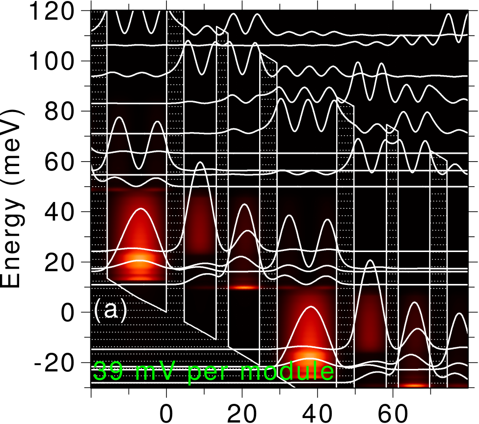
Specifically, we consider a Terahertz QCL structure, labeled V812, which was already studied in Fathololoumi et al. (2013). It shows lasing up to 199.3 K (with Cu waveguides), comparable to the current record of 199.5 K Fathololoumi et al. (2012) for a similar device with higher current density. V812 belongs to the family of three-well designs with resonant tunnel injection and resonant phonon extraction Williams et al. (2003), see the band-diagram at the nominal operation point (NOP) in Fig. 1(c). This class of designs has been previously shown to exhibit bias instabilities around threshold Fathololoumi et al. (2013), when operated via a serial resistance. This is due to NDC occurring for biases after alignment of the injector level with the lower laser and extractor level, as common for tunneling in semiconductor heterostructures Kazarinov and Suris (1971); Esaki and Chang (1974); Capasso et al. (1986).
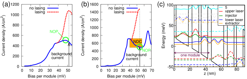
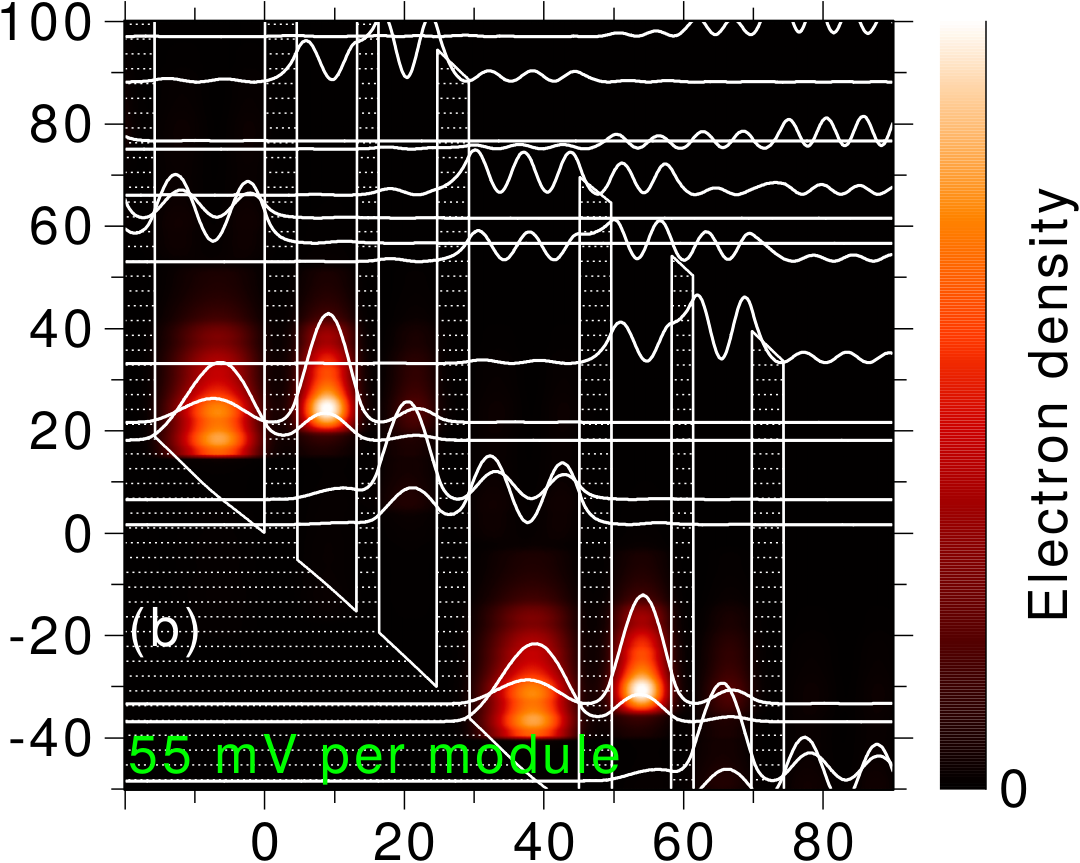
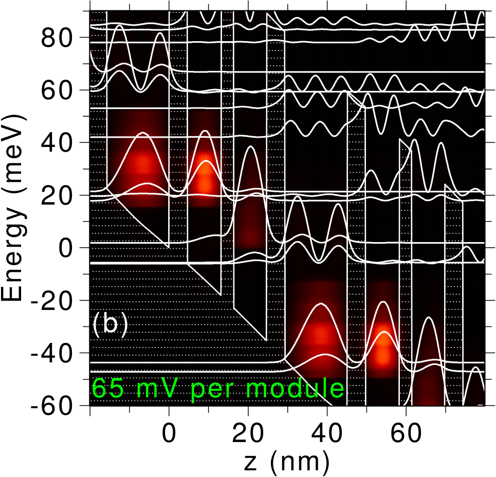
Fig. 1(a) shows the generally sought scenario where the QCL ignites in a region without NDC; this example is a highly performant bound-to-continuum four-well structure Li et al. (2014). After threshold, the lasing field causes stimulated emission, which enhances the current (dashed line) compared to the current without lasing (solid line). These data are obtained from our non-equilibrium Green’s function (NEGF) model Wacker et al. (2013); Winge et al. (2016), where we assume a homogeneous bias drop along the structure allowing for periodic boundary conditions between the modules. For the device V812, studied here, we instead find a current peak at a bias of 39 mV per module, which is below the NOP, see Fig. 1(b). Above this point, the current drops with bias resulting in a region of NDC, which even covers the NOP at 54 mV per module, where the injector level aligns with the upper laser level. Thus, without stimulated emission, the NOP is not directly accessible. However, the current starts to increase at a higher bias exhibiting a peak at 65 mV, where the upper laser level aligns with a further level 5 111For its most part, level 5 corresponds to the second excited state of the lasing double-well.. We will demonstrate how this tunnel resonance plays an essential role during laser ignition as it provides an operation point with positive differential conductivity exhibiting sufficient optical gain. For the self-consistent lasing field [red dashed line in Fig. 1(b)], where gain and losses compensate, the current is strongly increased, resulting in positive differential conductivity and stable operation around the NOP. This situation is in complete analogy with the scenario proposed for SLs Kroemer (2000). Comparing Figs. 1(a,b), we find that the ratio between the lasing-induced current and the background current is actually higher for the QCL operating in the NDC region. For the bound-to-continuum structure in Fig. 1(a) further current paths through other levels prevent NDC. This results in a parasitic background current density at the operation point which acts as a source of dissipation Chassagneux et al. (2012). For good diagonal designs such as the structure V812222The “diagonality” of a design is related to spatial separation between lasing states and is commonly assessed by the oscillator strength, here 0.3 in V812 structure. The lower the oscillator strength between lasing states, the more “diagonal” is the laser design., the current without lasing is actually low at the NOP, as a long life-time of the upper laser state is envisaged. Thus the scenario observed in Fig. 1(b) is actually beneficial, provided the ignition of the lasing field is guaranteed.
In this manuscript we show, how the ignition occurs in V812 by a detailed experimental and theoretical study. For this purpose we extend the standard simulation schemes for domain formation for superlattices Wacker (2002); Bonilla and Grahn (2005) and QCLs Wienold et al. (2011) by the interplay with the cavity fields, as taken into account by our microscopic NEGF simulations, see Appendix A.2. Using this model, we are able to simulate the ignition of the lasing field in the NDC region. The current-bias relation exhibits a “merlon” at threshold in good agreement with the experimental data as discussed in Sec. II. Studying the time-dependence of the experimental bias, we observe self-sustained oscillations on the GHz scale both before and after threshold, see Sec. III. Within our model, these oscillations are attributed to traveling field domains. Furthermore, we validate the ignition scenario by the red shift of the lasing spectrum close to threshold in Sec. IV. Details on the simulations and experiments are given in Appendices A,B, respectively. Appendices C,D provide additional data from simulations and experiments with a different device. Finally, Appendix E addresses the distortion of the oscillation signal by the incomplete RF design. Our findings clearly demonstrate the ignition scenario in the NDC region, which results in conventional lasing at the NOP, where the lasing induced current stabilizes the operation.
II Formation of field domains
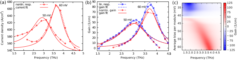
Fig. 2 shows an unusual scenario around ignition in the light()-voltage()-current density() characteristics, where the voltage has a flat local maximum (referred to as merlon) around as highlighted by the colored areas in panel (b). Simultaneously, the light intensity exhibits a peak, while at higher current density () a common linear increase of intensity and bias is observed. The results from our model with domain formation, see panel (c), agree reasonably well with the experimental observation in panel (b).
The global scenario leading to the merlon is shown in Fig. 2(a). The relation is obtained by operating via a load resistance and a parallel capacitance with an external bias –the output voltage from the pulser. (The circuit model is further discussed in the Appendix A.2.) If the load line is shifted to the right of the first current peak around 39 mV per module, a domain state is established in the QCL, which results in the red solid horizontal line, also called current plateau. Here the total bias is distributed on a low- and a high-field domain [shown in greater detail in Fig. 4(a)]. The high-field domain exhibits gain (at a frequency slightly higher than the NOP), and the total gain, as expressed by Eq. (7), gets close to the losses, if the high-field domain becomes large enough. The onset of lasing changes the local current-field relation, which gives rise to the pronounced merlon of the dashed red line. For even higher currents, this domain state merges with the homogeneous state under lasing (black dashed line) demonstrating that the conventional lasing around the NOP is stabilized due to the lasing induced current.
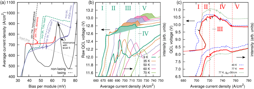
The merlon feature occurs for a wide range of temperatures up to 90 K in our sample, see Fig. 2(b). Both in experiment and simulation, it is shifted to higher currents with increasing temperature, see Fig. 2(b, c). In Fig. 2(c), we also show simulations for an increased threshold gain , which shifts the bias, but does not change the essential feature. Such a shift also occurs between devices with different metallization of the electric contact, see Fig. 2(a). A similar merlon is also observed between 89 K and 105 K for the structure V773 of Ref. Fathololoumi et al. (2013).
Around the merlon we identify five regions, as indicated in Figs. 2(b, c). In region I, increases with relatively little variation of current as common for domain formation, where the increase in bias corresponds to a spatial increase of the high-field domain. At the experimental threshold, we observe a kink in [together with a small spike (20 mV) in (b) at low temperature]. Subsequently, a joint increase of current and bias marks the region II, the left flank of the merlon. Both in experiment and simulation, the lasing intensity is drastically increasing in this region. This is followed by a region III, the top of the merlon, where the bias is almost constant and the calculated lasing intensity shows less variation, while a drop is observed in the experiment. The latter may be partially related to the drop in laser frequency occurring here (see Sec. IV) and associated changes in mirror losses. On the right flank of the merlon, region IV, the bias drops with current. Finally, in region V, the bias and intensity increase almost linearly with current as common for lasing operation within a homogeneous field distribution.
Fig. 2(a) also provides a comparison between the experimental characteristics of three devices, processed with either TiAu or PdGe contacts. The PdGe mesa device was purposely fabricated to frustrate stimulated emission. The of this device (purple solid line) shows two pronounced shoulders at average biases of 40 mV and 68 mV per module, without any detailed structure in between. This confirms our simulation data (black solid line), which show current peaks close to these biases, but, without lasing, no current peak at the operation point of 54 mV per module. Voltage fluctuations, as recorded with a 1 GHz bandwidth oscilloscope, are overlaid on the current density of the PdGe mesa device in Fig. 2(a). They can be regarded as a sign for NDC both between the shoulders and after the shoulder at 68 mV/module. Laser emission on the low loss waveguide, i.e. with TiAu contacts, collapses after 55 mV/module, close to the predicted NOP, a voltage corresponding to the optimum injection to the upper laser state, which is now accessible thanks to stimulated emission. This is in contrast with the higher loss waveguide device, i.e. with PdGe contacts, where laser emission switches off later, above 60 mV/module.
The simulated increase of current above 75 mV per module is due to tunneling from the lower lasing level to level 5 (aligned at 83 mV per module) and subsequent leakage to continuum. As the current in the continuum is not well covered in our model, the simulations underestimate the current here. Overall, the simulated current densities and biases agree well with the experimental data.
III Oscillating field domains
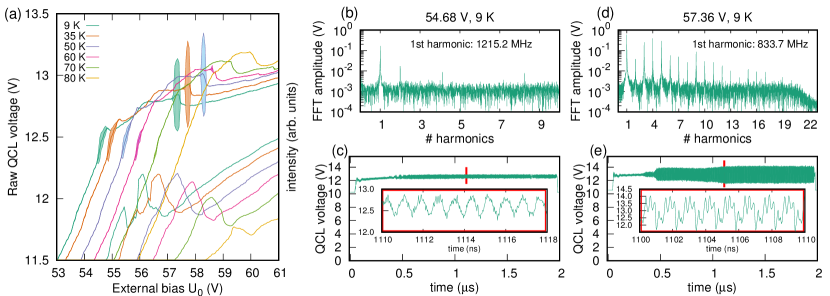
Fig. 3 shows self-sustained bias oscillations measured experimentally. As exemplified in panels (c) and (e), they occur both below and above threshold. The shaded regions in panel (a) show the extend of the oscillatory behavior as monitored with the 1 GHz bandwidth oscilloscope, see Appendix B. With a high bandwidth real-time oscilloscope, we observe GHz oscillations up to a temperature of 78 K in parts of region III and the transition to IV. Here, we measure frequencies in the range of GHz, which are decreasing with bias for each temperature. In region I, the less intense GHz oscillations are detected up to 68 K. The frequencies are around 1.2 GHz and increase up to slightly 1.3 GHz above threshold. The laser ignites while the voltage self-oscillates, nevertheless these oscillations are quickly damped as the bias increases above threshold (beginning of region II), see also Fig. 14 in Appendix D for the oscillations around threshold. The measurement of the bias dependence of the oscillation frequency is described in Appendix D.
The occurrence of oscillations with GHz frequency can be understood on the basis of traveling field domains as known from Gunn diodes Shaw et al. (1992) and superlattices Wacker (2002); Bonilla and Grahn (2005). For the low doping density, the NDC region cannot be overcome by charge accumulation in a single module Wacker (2002); Wacker et al. (1997). Based on the current and electron density, we estimate an average drift velocity of 6.6 km/s, with which these excess carriers between the domains travel through the structure. As a new accumulation layer forms only after the preceding one has traversed a large part of the device with a length of 10 m, we get a typical oscillation period of 1 ns.
Such oscillations based on traveling field domains are found in our simulations as shown in Fig. 4 for a selected set of operation points in the current-bias relation (extensive data can be found in Appendix C. Here we find different oscillation modes in the different regions of the current-bias characteristics, labeled I-IV in Fig. 4. The reason is that the local current-field relation is strongly modified by the lasing field.
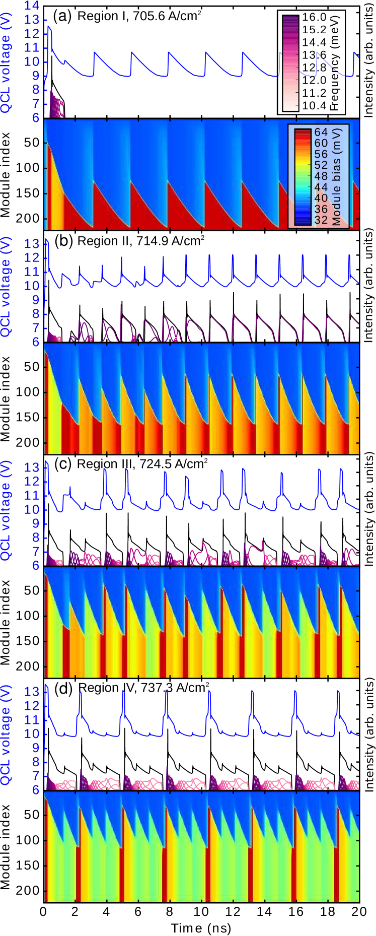
In region I, the lasing field does not play a role and the local current-field relation [as given by the black line in Fig. 1(b)] is unaltered. Within the domains, the condition of a constant current density implies the bias drop per module of mV and mV, in the low- and high-field domain, respectively. Between both domains, there is a layer of electron accumulation [e.g. around module 150 at 6 ns in Fig. 4(a)], which travels towards the positive contact. From time-resolved electron density plots we find that the accumulation layer spans over several modules (3-6). The movement of the accumulation front provides a drop in bias and, following the load line, an increase in current. Eventually, the current reaches the first peak in the local current-field relation, where the low-field domain becomes unstable and a new domain boundary forms (e.g. around module 130 at 8 ns). These oscillations exhibit frequencies of 0.4-0.6 GHz [as can be seen in Figures 10, 11 of Appendix C], increasing with external bias in accordance with measurements.
In region II, the lasing field is strong enough to alter the local current-relations resulting in the surge for the average current, see Fig. 2. Lasing sets in just after the forming of the high-field domain [e.g. at 12 ns in Fig. 4(b)]. The increased current results in a drop of field in the high-field domain, as conduction plus displacement current has to match the current in the low-field domain. In the following, the accumulation front travels, reducing the extend of the high-field domain and the total gain drops, so that lasing operation stops. While the accumulation front travels further, the low-field domain reaches the first current peak and a new domain boundary forms similar to region I.
Upon increasing the external bias to region III, the new instability may occur, while lasing is still active. Then the new high-field domain arises at a lower field around 50 mV per module [e.g. at 10 ns in Fig. 4(c)]. However, starting from this state, lasing always stops before the next domain forms and we observe an irregular (possibly chaotic, but we did not prove this) pattern in Fig. 4(c) or different types of locking between both scenarios, see Fig. 12 in Appendix C.
In region IV, see Fig. 4(d), lasing prevails most of the time and at least half of the high-field domains are formed close to the NOP with fields around 50 mV per module. This provides the drop in average bias as characteristic for this region. While new domains form about once per ns, the fundamental oscillation frequency is 0.37 GHz in Fig. 4(d) as only every third time the lasing operation stops.
Comparing with the experimental oscillations, the shape of the bias signal in region I is triangular both in experiment, Fig. 3(c), and simulations, Fig. 4(a). The bias signal in regions III/IV resembles more a switching between plateaus with bias values separated by 1 V. Here the experimental data, Fig. 3(e), do not show the thin bias spikes visible in Figs. 4(c, d). Instead, a strong ringing-like feature with a pseudo-period of ns is observed, which is attributed to lacking RF design (see Appendix B). An attempt to filter out ringing effects has been tested and some deconvolution results are reported in Appendix E. The simulated frequency of the oscillations in region I (0.5 GHz) is lower than the experimental results (1.2 GHz), while in region III the experimental frequency well matches the mean rate of domain formations (both 0.8 GHz). In region III, we also detected a subharmonic regime at a specific bias range, see Fig. 16 in Appendix D and Fig. 17(b) in Appendix E, which might indicate different coexisting domain ignition processes as observed in the simulations in regions III and IV. The main discrepancy is that the simulations provide oscillations throughout all the regions I-IV, while experimentally they are only clearly detected within parts of the regions I, III, and IV (the latter is small in the experiment), as shown in Fig. 3(a). However, we experimentally observed strongly enhanced noise on voltage, light intensity, and phase on the lock-in amplifier used during THz detection in regions II and III, which we could not fully explain yet. In this context, we note that the stability of domains depends both on the details of the electron distribution in the transition region between the domains, the nature of the injecting contact, and the external circuit (for instance the 50 Ohm coaxial cable was not considered in simulations). For these issues, we did rather simple approximations, which are difficult to overcome as no consistent treatment has been proven valid so far. Furthermore, pinning of the accumulation layer may occur if individual modules differ due to growth imperfections. These effects could also cause the differences between the measured and simulated oscillation frequencies.
IV Lasing Spectra
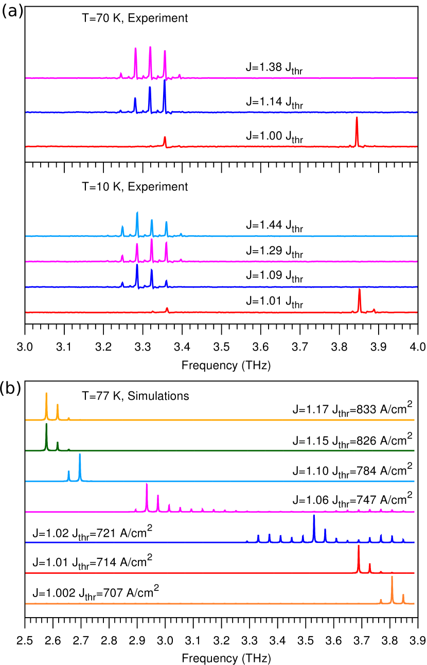
For the ignition scenario from a domain state discussed here, the high-field domain exhibits a higher bias drop per module than the final lasing state. Due to the Stark shift, which is substantial for a diagonal design as V812, we thus expect a higher lasing frequency at ignition. Fig. 5 shows that this is indeed the case. Just after threshold, the lasing frequency is around 3.8 THz in the experiment and slightly lower in the simulation. With increasing current a drop to 3.3 THz (experiment) or 2.6 THz (simulations) is observed, where the frequencies remain constant with further increase of current. The discrepancy in frequency for operation in region V is related to the lower threshold bias in the simulations. Fig. 2(a) shows, that the lasing around 800 A/cm2 occurs at 45 mV per module in the simulations and at 50 mV per module in the experiment. Thus the difference in frequency corresponds to the Stark shift. E.g., for an operating bias of 52 mV per module, the simulations show a gain peak at 3.1 THz (see also Fig. 8 in the Appendix A.3) in much better agreement with the experimentally observed lasing. A similar spectral red-shift after threshold was also observed in the more diagonal structure V773 of Ref. Fathololoumi et al. (2013).
V Conclusion and Outlook
The onset of lasing from a state of oscillating electric field domains was demonstrated for THz QCLs. Comparing experimental and theoretical results, this feature is clearly reflected in the shape of the current-bias relation, characteristic self-sustained oscillations around threshold, and the red shift in the optical spectra just after threshold.
This ignition type demonstrates that there is no need for positive differential conductivity for the NOP at threshold, which is also visible in other highly performing QCLs Chan et al. (2013); Fathololoumi et al. (2013). Instead, significant gain at a resonance at higher field is sufficient. In this case domain formation in the NDC region allows a part of the device to operate at this auxiliary operation point. After ignition of the lasing field, the stimulated transitions provide sufficient current at the NOP to break the NDC. Thus a conventional requirement for laser design is lifted, which allows for more flexibility in the design of QCLs at the price of noise-like behavior at threshold. In particular, such a new design could reduce the background current and provide more effective power conversion to the lasing field. In order to realize this scenario, during the design stage of highly diagonal structures particular attention should be paid to the gain at the positive differential resistance region next above the NOP.
Furthermore, we found complex oscillation patterns due to the interplay between the lasing field and the running field domains. This establishes a further degree of freedom compared to the related superlattices with their rich spectra of nonlinear and chaotic behaviorAmann et al. (2003); Fromhold et al. (2004); Hramov et al. (2014). In this context the time-resolved measurement of the lasing activity with a fast THz detector Scheuring et al. (2013) could provide additional relevant data.
Acknowledgements.
The authors would like to thank Dr. Saeed Fathololoumi for the FTIR measurements and Dr. Seyed Ghasem Razavipour for fruitful discussions and for providing unpublished data on wafer V773 collected in the lab of Prof. Dayan Ban, Waterloo University. Dr. Sergei Studenikin and Nick Donato from Tektronix have kindly lend us the 15 GHz and 2 GHz bandwidth oscilloscope, respectively. Financial support from the Swedish Science Council (grant 2017-04287) is gratefully acknowledged.Appendix A Simulation procedure
A.1 NEGF simulations for homogeneous field distributions
Our calculations are based on the NEGF model Wacker et al. (2013); Winge et al. (2016) providing us with the current density and gain which are nonlinear functions of the electric field . Here is the field due to an applied bias and is the electrical component of the lasing field in the waveguide with frequency . As common for most simulation schemes Jirauschek and Kubis (2014), these calculations assume a homogeneous bias drop along the QCL structure. To calculate the current under operation we increase the ac field strength at each bias point until gain is saturated by the level of the losses . In addition, the peak gain frequency is updated with the ac field strength to track intensity dependent effects on the laser transition. This procedure provides the data presented in Fig. 1(a,b). The temperature used in the simulations defines the thermal occupations of the phonon modes. Due to the excitation of the mostly relevant optical phonons on short time scales Vitiello et al. (2012); Shi and Knezevic (2014) this temperature should be higher than the experimental heat sink temperature. As input we use the nominal sample parameters together with an exponential interface roughness modelFranckié et al. (2015) with 0.2 nm height and 10 nm lateral correlation length. All these model details agree with Winge et al. (2016), where results for a large number of devices are shown. Note, that we define the bias , electric field and electric current(density) with an additional minus sign throughout the paper to compensate for the negative electron charge .
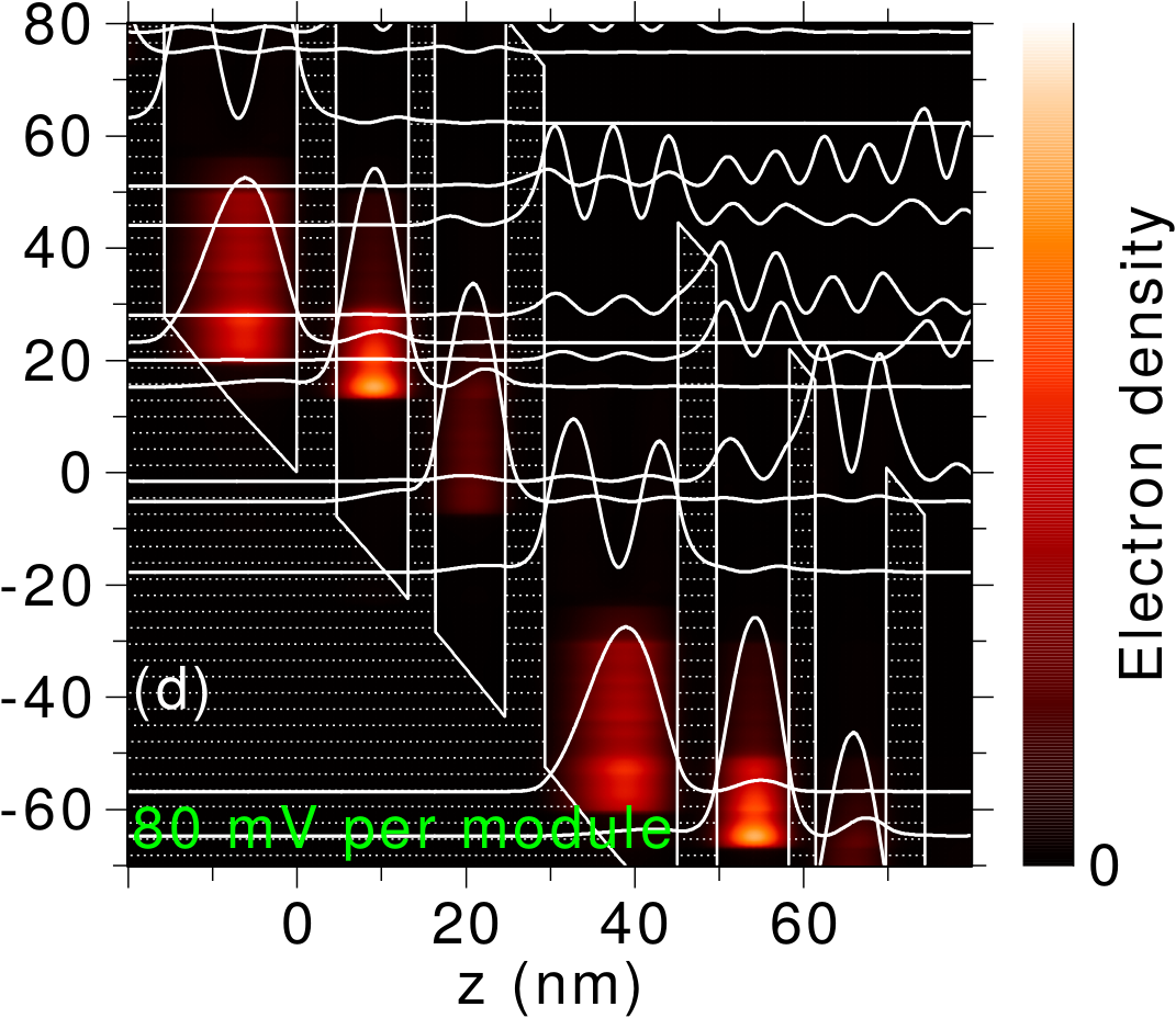
In Fig. 6 we show the calculated electron densities together with the Wannier-Stark levels for different biases, in order to study the relevant alignments. For a bias of 39 mV per module (panel a) the injector states aligns with the lower laser level and the extractor state allowing for a strong current through the entire module. This is just the first current peak in Fig. 1(b). The resonance at 65 mV is shown in panel (c) and the increasing current around 80 mV [see Fig. 2(a)] is attributed to tunneling to continuum states in panel (d). Here, we used 9 states per module and next-nearest neighbors in the simulations. For biases below 70 mV per module, we found that 7 states per module were sufficient, which allows to reduce the numerical effort.
In order to simulate domain formation with the interplay of an intra-cavity lasing field, as shown in Fig. 2, the gain needs to be estimated at frequencies , which may differ from of the lasing field. A common situation in this study is that lasing sets in in the high field domain, allowing for a build up in intensity at the frequency favored at that field strength. As intensity increases, the local current-field relation changes to a degree, where lasing at other frequencies is more favorable compared to the original one. This poses the question: How does the established laser field promote the onset of lasing at other frequencies? To answer this, multidimensional fitting of the simulated NEGF data is not enough, as we need to estimate the gain at frequencies other than the lasing frequency. Our approach is to use fits for the current density and gain which are based on a simple physical model (see Appendix A.3) and where the parameters are determined by comparing with the full NEGF calculations.
A.2 Domain formation and external circuit
In this section, we describe the simulation of the extended QCL structure with modules within the circuit shown in Fig. 7(a).
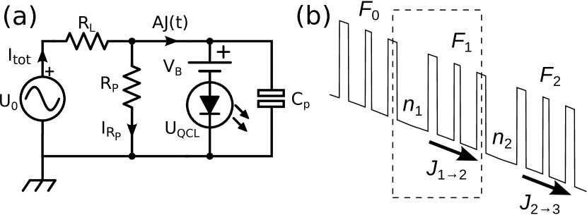
In particular, we drop the assumption of a periodic voltage drop along the QCL structure, which lifts the requirement for charge neutrality in each module of the QCL. Instead, the electron density in module may differ from the background doping (both in units 1/area). Here we assume that the additional charge of each module is essentially located in the injector well [the widest well of the structure, see Fig. 1(c)], and that the current density between the injector wells and essentially depends on the bias drop over module . The numbering is illustrated in Fig. 7(b). Following Ref. Wacker and Schöll (1995), Ampere’s law and Poisson’s equation provide
| (1) | ||||
| (2) |
where is the current density flowing into the QCL device and is the intrinsic QCL capacitance assuming an average relative dielectric permittivity for the active region with the cross section and a module thickness nm. We use the parasitic capacitance and checked explicitly that larger values like hardly change the results. Operating via a load resistor , the circuit in Fig. 7(a) provides
| (3) | ||||
| (4) |
where is the Schottky barrier and is the voltage probe resistance. Throughout the paper we use Ohm, Ohm, and in our simulations. The load curve of Eq. (3) does not consider the effect of the residual resistance of the ground electrode on Si carrier, as addressed in Appendix B. Determining the current density within a module is far from trivial, as we have to take into account a non-periodic situation and carrier densities differing from the doping. Following the common approximation for superlattices Wacker (2002); Bonilla and Grahn (2005) and QCLs Wienold et al. (2011), we use
| (5) |
This expression is only defined for , as a real injector well is required on both sides. In order to close the equation system, we further need the cases and . Here we assume Ohmic boundary conditions
| (6) |
with the conductivity , which is chosen to be higher than the average conductivity in the QCL structure. This modeling follows essentially Wienold et al. (2011), where domain formation in QCLs was studied. Going beyond this work, we also consider the coupling to the lasing field here.
The waveguide modes constitute a global coupling between the modules. Each mode is associated with a constant frequency , an electric field strength , and its average photon number . Similarly, the gain in the waveguide is obtained by the average over all modules, where we assume that the gain is proportional to the electron density in the respective module:
| (7) |
Here the gain in each module is subject to saturation from all cavity modes. The gain recovery time is given by the time-scales for scattering and tunneling in the modules, which are typically ps. This is shorter than the photon lifetime of 6 ps (for the gain threshold of ), so that we can assume, that the gain is an instantaneous function of the intensity. For the photon numbers we thus have
| (8) |
for all cavity modes , where is the group refractive index (assumed to be constant here), and is given by the waveguide and mirror losses. A similar approach to model the photon density in a THz QCL was reported in Ref. Agnew et al. (2015).
The last term in Eq. (8) describes the spontaneous emission of light from electrons in the upper laser level into the lasing mode , which is crucial for ignition. Assuming a plane wave in our metal-metal waveguide, we can use the standard textbook expression for the spontaneous emission rate [see, e.g., Eq. (8.3-6) of Yariv (1988)]
| (9) |
where is the matrix element between the upper and lower laser state, m is the thickness of the waveguide, and is the Lorentzian from Eq. (11) replacing the delta function. For different operation points, we find typical values ms. For simplicity we choose ms for all simulations. This value is appropriate for the high-field domain with meV, where lasing typically sets in. (Here is large and is small, see Fig. 8). We checked explicitly, that increasing by a factor of two hardly changed the results.
A.3 Effective model of a single module
In order to fit the current and the gain, we use expressions resulting from a simple two-level model, onto which the NEGF results are mapped. We consider an injecting current into level 2, scattering lifetimes , for level 1 and 2, respectively, and for scattering from 2 to 1. A laser field closely resonant to the energy difference induces a transition rate, which, according to Fermi’s golden rule Sakurai (1993), is proportional to the square of the oscillating field:
| (10) | ||||
where the energy-conserving -function is replaced with the more realistic Lorentzian
| (11) |
Under irradiation with we can thus establish the rate equations, following Ref. Faist (2013),
where the second term of the equation for makes sure that the population reaches its thermal equilibrium value in the absence of the injecting current and ac field. For the steady state, we obtain the inversion
| (12) |
where right hand side of the first line corresponds to the inversion for vanishing ac field strength. Thus
| (13) |
with as the ratio should be minimized for a good QCL design. Following Ref. Wacker (2012), we can relate the linear response gain for a two level system to the -factor as
| (14) |
Following Ref. Lindskog et al. (2014), Eq. (13) provides the gain saturation
| (15) |
Here, is the unsaturated linear response gain from Eq. (14) with . Note, that we have now separated the pumping ac field at frequency from the probe at , which means that we can now probe the saturated gain at a chosen frequency going beyond our NEGF simulations, where only a single frequency appears.
Under the assumption that the bottleneck for current is the inverted population at the laser transition, the total current will be a sum of stationary and induced current following
| (16) |
where only the frequency , saturating the system, appears. Here, we use the absolute value of the inversion, following our observation, that the current also increases with absorption in the NEGF simulations, due to new transport channels opening up. The expression can readily be generalized to many modes of finite intensity, yielding a sum over field strengths at different frequencies , each with . Identifying the gain in the expression for current, using Eq. (14), gives
| (17) |
where the total gain contains a sum over the relevant transitions. The last factor in the first equation has been rewritten as the Poynting vector giving the intensity at in the final expression.
To map the NEGF simulation results onto the effective model, we first calculate and for vanishingly small at each bias point . We consider the range of 35 – 65 mV per module and frequencies 1.5 – 4.5 THz as relevant for domain formation. is fitted by and . According to Eq. (15) the saturated gain can then be described by the effective lifetime , which is found from fitting the gain spectra to the NEGF simulations at higher intensities, as exemplified in Fig. 8(b). We thus require three fit parameters (), together with the calculated and to model the saturated gain and current at each bias point. Here, the NEGF simulation data is fitted to a target function consisting of both Eq. (15) and (17) which balances both the gain and stimulated current contributions and makes efficient use of all simulation data. The procedure provides a physically sound way of interpolating through the simulation data and allows us to calculate the current under irradiation as a function of bias, frequency and ac field strength. Representative current and gain spectra are shown in Figs. 8(a) and (b), respectively, together with their fits using Eq. (17) and Eq. (15).
Figs. 8(a,b) shows a particularly large linewidth for a bias of 50 mV per module. The reason can be seen in in Fig. 6(b), where the lower laser level and the extraction level form a doublet with a spacing of 5 meV. Thus the gain is based on two different transitions of approximately equal strength resulting in the large linewidth.
Unsaturated gain for a single module as a function of bias and frequency is displayed in Fig. 8(c). A strong Stark shift can be seen as bias is increasing. At the nominal operation point of 54 mV per module, gain peaks around 3.3 THz, which agrees with the experimental lasing frequencies reported in Ref. Fathololoumi et al. (2013), see also Fig. 5.
Appendix B Experimental methods and measurements
We consider the structure V812 reported in Ref. Fathololoumi et al. (2013) using devices processed with a Au-Au double metal waveguide. These showed lasing up to the heat-sink temperature of 160 K. The laser under study, 1.049-mm long and 143- wide, is Indium-soldered onto a highly resistive ( Ohm.cm) hyper pure floating zone Si carrier on which fan-out Au electrodes were fabricated, see Fig. 9(a). Laser devices and simple mesas (non lasing) with Pd/Ge/Ti/Pt/Au Ohmic contacts were also fabricated and mounted on Si carrier.
It occurred that both lasers, TiAu and PdGe contacted, were mounted on carriers with too thin electrodes that showed residual, although non negligible, resistance. The effect of the ground electrode resistance on measurements could not be circumvented easily, at least not in pulsed mode operation. Fortunately, the PdGe mesa devices were mounted on a carrier with much thicker electrodes (hence their vanishing resistance) and their electrical characteristics served as reference in order to derive the ground electrode resistance of the Si carrier, the Schottky barrier (for TiAu only) and therefore the exact bias per module on laser devices [Fig. 2(a)]. Consequently, in Fig. 2(a) the experimental average bias per module for the PdGe contacted mesa device is simply given by the signal from the voltage probe divided by . This is in contrast with lasing devices, where the potential drop across the ground electrode resistance of 1 Ohm (TiAu, dashed green) and 0.85 Ohm (PdGe, dashed purple) of their “defective” Si carrier, as well as the Schottky top contact drop of 0.65 V for TiAu device, had to be taken into account. It is worth mentioning that the PdGe mesa device was tested in voltage-controlled conditions, i.e. with a small load resistance Ohm, which could explain why the current plateaus are not very flat (Fig. 2(a), purple solid line). In Figs. 2(b), 3(a,c,e) the “raw” QCL voltage is not corrected from the effects of Schottky barrier and ground electrode resistance of Si carrier; the latter is likely to be temperature dependent. This explains to a large extend the difference between the vertical scales of Fig. 2(b) and (c). Nevertheless, the overall good agreement between theoretical and experimental biases per module can be appreciated in Fig. 2(a).
High precision characteristics were recorded using current controlled conditions, by use of a series resistance of Ohm placed near the device in a 9 K closed-cycle He refrigerator system, see Fig. 7(a) for the circuit. The external bias is supplied to the circuit by a pulse generator. The total current in the circuit, , was measured at the output port of the pulse generator with a calibrated 200 MHz bandwidth current transformer. Because of the high resistive Si carrier, the device is operated with a floating ground. We made sure and checked that the net current in the 50 Ohm coaxial cable from the voltage pulser is zero, meaning the current flowing in the QCL returns to the pulser ground via the shield of coaxial cable.
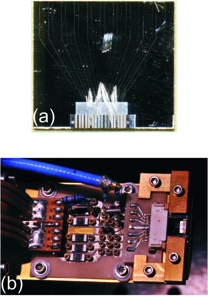
The voltage across the QCL, , is recorded via a four-point measurement setup and with a calibrated voltage probe placed inside the cryostat and terminated to 50 Ohm on the oscilloscope. The probe consists of a 18 GHz bandwidth SMA cable on which small footprint 1000 and 330 Ohm resistors were tightly soldered to center conductor and shield respectively. Despite the high quality SMA cable used here, the RF performance of the voltage measurement setup is hindered by the absence of RF design between the input port of the voltage probe and the device that are 25 mm apart, see Fig. 9(b). Before reaching the voltage probe, the RF signal has to propagate through simple wirebonds connecting the QCL electrodes and the tip of fan-out electrodes patterned on Si, then through non-RF designed fan-out electrodes on the Si carrier, then conductors on two AlN boards and finally the resistors used for the voltage probe. This incomplete RF design results in a ringing effect that is partially filtered out in Appendix E. In the future, a proper RF designed setup to probe the QCL voltage should be considered.
The small bypass current in the voltage probe (see Fig. 7(a)), was subtracted in the final reported results of current density in Fig. 2(b), in DC mode, and its resistance, , was taken into account in the load curve that is explained with Eq. (3) in next section, see also Fig. 7(a). The total circuit current and the QCL voltage were measured in pulsed mode with 2-s pulses, repeated at 100 Hz frequency and with 14 Hz macro modulation of the train of pulses to adapt the measurement to the response time of the Golay cell, the THz detector. The output of the Golay cell was connected to a lock-in amplifier with 1 s time constant and locked to 14 Hz reference signal. Here, unusual long pulses were used to benefit from the good flatness of these pulses in their second half and consequently report high accuracy data and longer sections of oscillations, when they occur. Small heating effects on laser threshold have been identified and found responsible for vertical () shift of the merlon for long pulses, the shift depending on the position of integration window where current and voltage are monitored. Experimentally, we observed the merlon at lower bias, if shorter pulses are applied (about 0.1 V lower for 300-ns pulse duration). This is why the electrical characteristics (Fig. 2(a, b) for instance) were recorded near the center of the 2-s pulse, not close to the trailing edge. A 5 GS/s, 1 GHz bandwidth digital oscilloscope (Tektronix DPO4104) was used to zoom and measure the top of the pulses and by using appropriate DC offsets and vertical scales. The and values were measured inside a 200-ns long integration window defined between cursors placed at and inside the pulse. Sixty four current and voltage traces were averaged (average mode of oscilloscope) and finally reported with 1 and 2 mV/div scales respectively, meaning that any changes of vertical scale that can result into discontinuities were taken into account and thoroughly corrected. Before turning on the average mode on the oscilloscope, clipping the single pulse signals (observed in sample mode) by the 10-division vertical dynamic range was carefully avoided in the integration window (only). The calibration of the pulse generator was also checked as well as that of the oscilloscope. Data from oscilloscope and lock-in amplifier were recorded 32 times, 1 s apart, and finally means and standard deviations were derived. We used 50 mV voltage steps on the pulse generator in order to resolve features on the merlon. At each step, we also recorded 200 single traces, i.e. non averaged (sample mode), of and channels to capture any oscillations or discontinuities. The median value of peak-to-peak amplitude of these pulses was computed inside the same 200-ns window of interest. Moreover, this median value was subtracted from the peak-to-peak amplitude of 64-pulse averaged signal to account for non perfect flatness of voltage and current channels in the integration window. After this subtraction the final value was named the “net” amplitude, which is shown for the entire temperature range in Fig. 3(a) superimposed on the bias signal as shaded regions. Note, that these amplitudes are only qualitative due to the limited bandwidth of the oscilloscope used here. When voltage oscillations were detected, current oscillations were also observed albeit less intense due to limited bandwidth of current transformer.
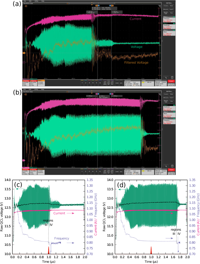
The time-resolved voltage oscillations were recorded with a 40 GS/s 15 GHz bandwidth real-time oscilloscope (Tektronix TDS6154C) and a 10 dB attenuator was employed due to the large oscillation amplitude in region III. The first set of measurements with the 1 GHz oscilloscope permitted to locate the oscillations with a low vertical resolution as a function of external bias. With the help these low resolution “spectra” we drove the time-resolved measurements with TDS6154C for different external biases and temperatures; single pulses were sampled at a maximum resolution, 25 ps/point.
Due to the residual positive slope of the external bias from the pulser (), single pulse measurements could reveal several sections of the merlon at once (such as regions III and IV). This simple technique, described in Appendix D, was convenient to assess the oscillating frequency versus raw QCL voltage.
The spectral measurements were performed with a continuous scanning Fourier transform infrared spectrometer set at a mirror velocity speed of 0.05 cm/s and resolution of 0.1 and equipped with a LHe cooled Si bolometer. We used a double modulation technique in which the QCL was biased with 0.5- pulses at a repetition rate of 300 Hz. The signal from bolometer was filtered with high pass 200 Hz filter and finally sent to lock-in amplifier with time constant of 10 ms. Only five or ten scans were accumulated by FTIR.
In passing we also note that high resolution X-ray diffraction measurements indicate that the experimental layers are 1.7% shorter. For thinner wells, the tunnel resonances are shifted to larger biases and the lasing transitions to higher frequencies, which might reflect some minor discrepancies observed between theory and experiment.
Appendix C Additional modeling results
To complement the data shown in Fig. 4, a set of plots detailing the domain formation simulation results are shown in Figs. 10-13. They describe the simulated oscillations from just before threshold to a highest current density of 1.07 , corresponding to a change in external bias, , from 54.2 V to 57.8 V, respectively. At the high end of the current, see Fig. 13(g, h), the lasing is stabilized in the sense that the high-field domain always stays close to 50 mV/per period and the laser action is uninterrupted. Increasing the external bias further, this state will eventually merge with the homogeneous branch as shown in Fig. 2(a).
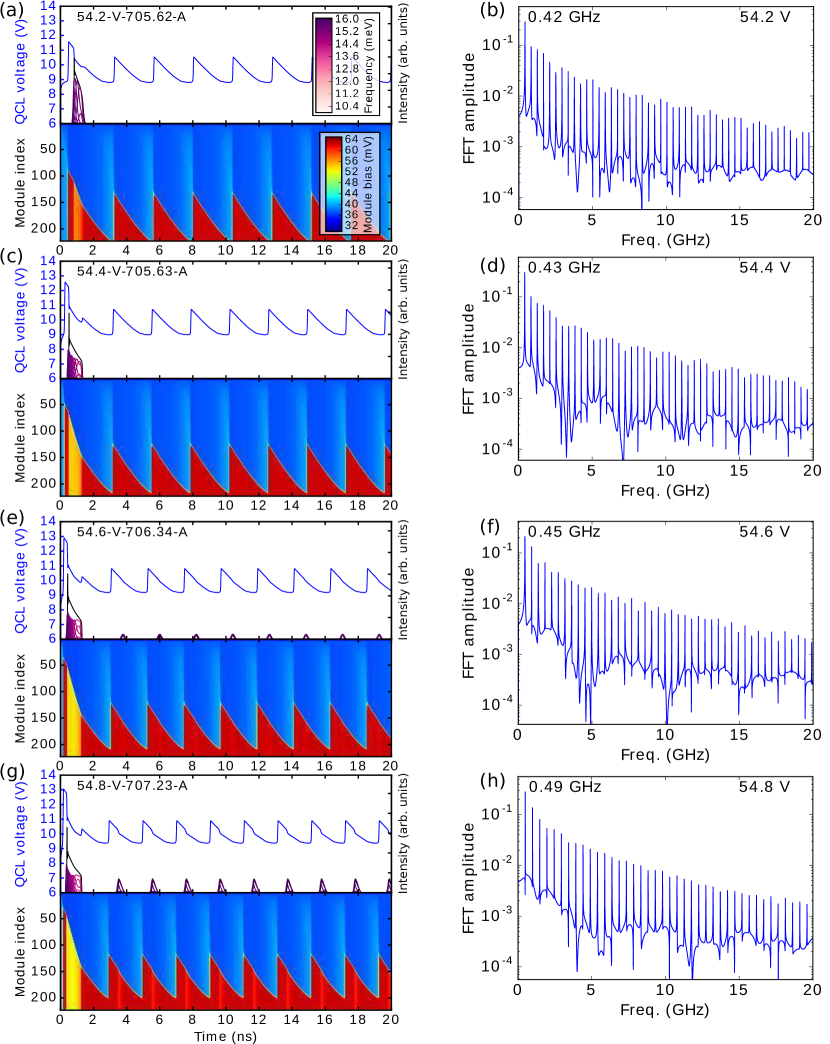
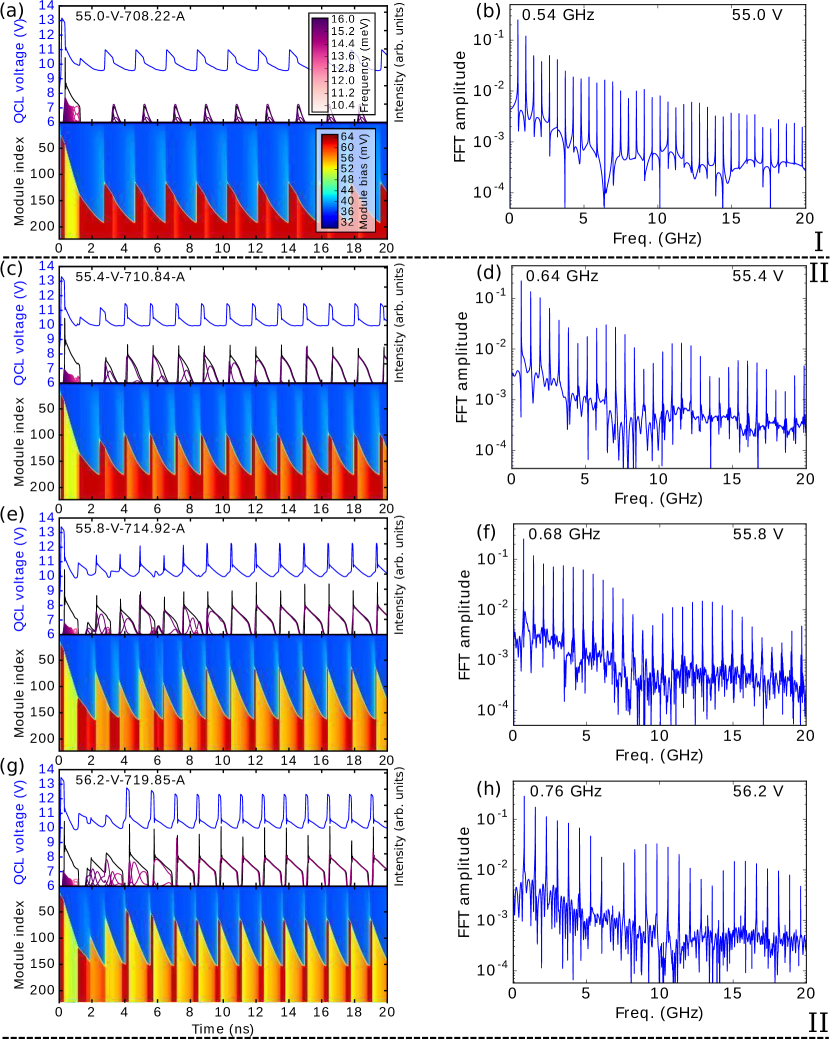
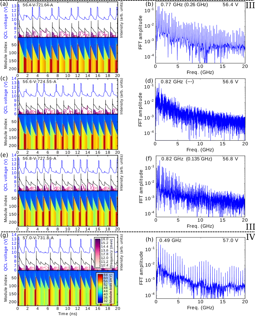
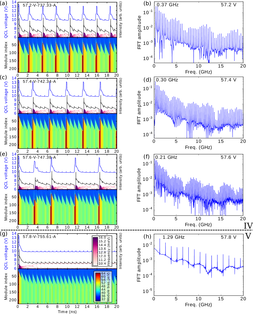
Figure 10 focuses on the oscillating domains of region I. Here the oscillation frequency is slowly increasing with bias as the new instability occurs at a larger extend of the previous high-field domain. Thus, the accumulation front travels a shorter range, resulting in the frequency increase with . The Fourier transforms (FTs) in the right hand column were taken over a long signal (200 ns) compared to short stretch of time of only 20 ns used for the voltage and module color plots on the left side. In each of the panels the frequency of the strongest oscillating signal is given together with the lowest frequency distinguishable in brackets. In panels (e, g) threshold is actually reached for short periods in time, but the lasing field is too weak to influence the local current-field relation. Thus the high-field domains keep the field strength of 62 mV per module.
Figure 11 shows the transition from region I to region II, where the lasing strongly increases and affects the high-field domains, whose fields drop. Due to the Stark shift, this implies a drop in lasing frequency, and lasing is now also observed for lower frequencies, see also Fig. 5. However, lasing stops, after the high-field domain has shrunk sufficiently due to the traveling accumulation front. On the right hand side, we note an increase in the oscillation frequencies.
The next collection of plots in Fig. 12 shows the region III and the transition to region IV. Here the lasing is still active while some new high-field domains form with a field of 50 mV per module, i.e. close to the NOP. Thus two different domain formation scenarios coexist. These do either arrange in a pattern such as in panels (a, b) and (e, f) with subharmonic frequencies and , respectively, or become irregular as seen in panel (c, d). A similar subharmonic feature could also be detected experimentally, see Figs. 16 and 17(b) below. Within region III, where the average bias drop over the QCL is roughly constant, less than half of the new high-field domains exhibit this low field. For the lowest panels (g, h), the two different domain formation processes alternate. For this operation point, the average bias reaches a maximum, defining the transition to region IV.
In the final collection of plots in Fig. 13 decreasing oscillation frequencies of region IV can be studied, where the interruptions in lasing become less and less frequent. As field-domains with high field become rare, the average bias drops in this region upon increase of the total bias , which defines region IV. In the lowest panels (g, h) the lasing is uninterrupted and region V is reached, where the laser operates with a linear increase of bias and intensity with current. Our simulations show some oscillatory feature. However the amplitude of the bias oscillation is strongly reduced compared to the other regions.
Appendix D Bias dependence of oscillation frequency
The voltage dependence of the oscillation frequency can be demonstrated by repeating the measurement of the raw QCL voltage with the 15 GHz bandwidth oscilloscope at different external biases . However, this obvious measuring technique was hampered by the pulse-to-pulse variations. Therefore, a faster method was also employed which relied on the residual positive slope of the voltage input pulse and a local Fourier transform within a Gaussian window covering 40 ns. This slope is non negligible for and is greatly reduced at longer time as the external bias eventually converges to the setpoint value.
In the set of experiments reported in the Appendices D and E we used actually a different device than the one in Sec. II and III. This device is from the same laser bar, mounted on the same Si carrier, and its electrical characteristics, the merlon for instance, are very similar. However, the bias oscillations were stronger with a peak-to-peak value up to 3.6 V as monitored by the 15 GHz bandwidth oscilloscope.
For the data reported here, we employed a 6.25 GS/s, 2 GHz bandwidth oscilloscope (Tektronix MSO58) with its 8-bit analog-to-digital converter to benefit from its maximum sampling rate. A digital low-pass filter with a cutoff frequency of 312.5 MHz was available, which allowed the real-time visualization of changes in average bias as characteristic for different regions in the merlon. By carefully adjusting the setpoint on the pulser, we could observe the oscillations in region I with the transition to region II, see Fig. 14(a), as well as the oscillations in region III with the transition to region IV, see Fig. 14(b). Fine tuning of the pulser setpoint and a “judicious” choice of the pulses –due to inevitable pulse-to-pulse fluctuations– were necessary to obtain this data.
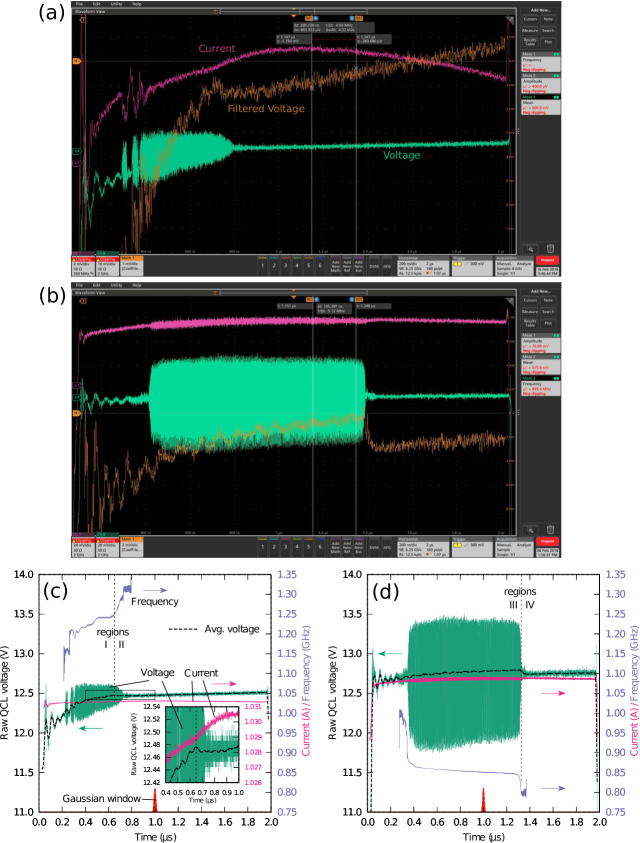
Figure 14 shows two examples of oscillations at 9 K for external bias corresponding to regions I [nominal pulse amplitude V, panels (a, c)] and III [ V, panels (b, d)]. The panels (a) and (b) are the oscilloscope screen captures of the total current pulse (magenta), the raw QCL voltage (green) and the low-pass filtered voltage (orange). The bottom panels (c) and (d) show the results of a moving Fourier analysis performed on the raw QCL voltage. For that purpose, a 45 ns (panel (c)) and 40-ns (panel (d)) wide Gaussian windows with a center shifted from the leading to the trailing edge of the pulse were used. The standard deviation of the Gaussians were 7.5 ns and 6.7 ns respectively. Doing so, in a single shot, the average voltage within the Gaussian window (black line) can be computed and the voltage sensitivity of the first harmonic frequency (purple line) estimated, albeit the non flatness of external bias pulse might slightly influence the oscillation frequency.
In Fig. 14(a, c) we identify the transition between regions I and II at by the sudden change in slope in bias, which stops its strong increase. More detailed, the inset of panel (c) displays a small spike in bias (10 mV), similar to the one observed at threshold for low temperatures in Fig. 2(b) where the spike is 20 mV in average mode. Furthermore, a slight increase in the current slope also indicates the transition to a region with higher average conductivity as common for region II due to lasing. These features are similar for all pulses analyzed. Regarding the lasing signal, we observed that the phase of the lock-in amplifier starts to be stabilized, when the oscillations vanish at the end of the pulse (strictly speaking for the majority of pulses with nominally equal set point bias ). Fig. 14(c), which is representative for many pulses analyzed, shows that the oscillations are decaying in time after entering the region II. This relates the transition between region I and II with threshold, see also Fig. 2(b). Therefore, laser threshold occurs in a state of running electric field domains, a likely hypothesis that could be confirmed with a fast THz detector Scheuring et al. (2013). Consequently, for the device is operated in region I, where we observe oscillations with a peak-to-peak amplitude of 0.4 V and frequencies of 1.2 GHz, slightly increasing with bias. These values agree well with the data in Fig. 3(b, c), where a different device was studied with a 15 GHz oscilloscope.
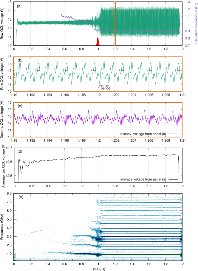
In Fig. 14(b) the sharp drop of filtered voltage (orange) indicates region IV, the only region where the bias over the QCL drops. This allows the identification of region III for times s, see also panel (d). Within this region large amplitude voltage oscillations with peak-to peak amplitude of 1.8 V and a frequency of 0.85 GHz, decreasing with bias, are detected by the 2 GHz oscilloscope (with the 15 GHz oscilloscope higher amplitudes are resolved). These values are again comparable to Fig. 3(d, e). The oscillations are also echoed in the current signal despite the current transformer being limited to a 200 MHz bandwidth. We observe, that this region is very sensitive to the bias pulses as shown in Fig. 15. The envelope of oscillations varies greatly from pulse-to-pulse and we see variations from day-to-day. Nevertheless the key issues are pertinent: i) the giant amplitude of oscillations of several volts, ii) the oscillation frequency consistently in 850 MHz range333The same 850 MHz oscillation frequency was automatically computed by the oscilloscope between the vertical cursors and displayed as “Meas 3” on the right side of the screen capture in Fig. 14(b). and iii) an averaged voltage drop V within the region IV. While the voltage drops, the oscillations actually persist, albeit with reduced amplitude. This is best seen in Fig. 15(a, c).
It is noteworthy that the pulse-to-pulse variations sometimes lead to a region III consisting of several segments with different amplitudes and with decreasing center frequencies, see Fig. 15(c, d). The moving FT results in an instantaneous frequency versus time that looks like a staircase, where the last step is centered at 813 MHz. When such a multi-segment region III appears it is also concomitant with a deeper average voltage step in region IV.
Analyzing the operation point with a raw QCL voltage of 12.65 V in region III in more detail with the 15 GHz oscilloscope, we could actually observe subharmomics , see Fig. 16. For larger values of , we observe this subharmonic regime systematically, when the QCL bias crosses the 12.65 V level.
Appendix E Filtering the oscillation patterns by deconvolution
For a better interpretation of the large amplitude oscillations of the raw QCL voltage observed in region III (see Fig. 3(e) and Figs. 14-16), the step response of the voltage probe setup was measured by employing a 200-ps rise-time pulser. In that way the setup was characterized up to 7 GHz. During this test, the load resistance was removed and the bias setpoint V was chosen to match the 50 Ohm DC impedance on the QCL at this bias. This measurement revealed a general ringing enveloppe at 0.93 GHz with a exponential decay of 1.1 ns, but also some complex features inside this enveloppe. From classic Fourier analysis we could reconstruct an estimated impulse response of the voltage detection setup. The impulse response shows complex ringing effects that we could not associate with simple electrical circuits. This response lasts for 3 ns and it is peaked at ns after the impulse. When integrating the impulse response, which is equivalent to derive the step response, the ringing effect would cause a strong 75% voltage overshoot at ns. With such an impulse response and by employing standard Fourier analysis we tried to perform deconvolution on the complex oscillation traces of the raw QCL voltage. Nevertheless, the results of this operation should be treated with cautiousness considering i), the RF circuit of the setup is far from being optimized as already explained in Appendix B and illustrated via Fig. 9 and ii), our characterization technique is limited to 7 GHz so far.
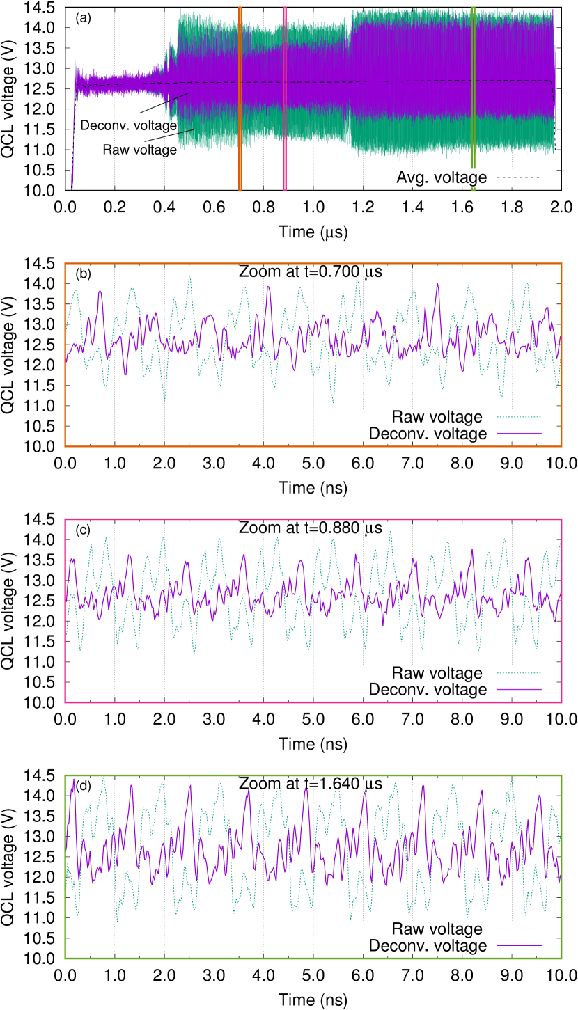
Figure 17 shows the result of deconvolution for an external bias corresponding to region III. The span of oscillations does not last 2 because of the residual positive slope of the input pulse (see Appendix D). Panel (a) demonstrates a reduction of the peak-to-peak amplitude oscillation after deconvolution, suggesting the ringing effects have been filtered out to a large extend. The next three panels show 10-ns wide zoomed areas representing segments, with different oscillation amplitudes in panel (a). From a bird’s eye view the raw QCL voltage patterns in the different segments look similar as ringing effects dominate; nevertheless, after deconvolution the differences become more evident. When the average voltage is 12.65 V we systematically observed a subharmonic regime, where GHz is the main oscillation frequency (Fig. 17(b) and Fig. 16). The filtered trace seems to indicate there could be one strong “spike” of voltage once every three periods. Such complex oscillations with three different spikes in a lapse of time, have been predicted by our model, see Fig. 12(a-b), and our filtered voltage trace resonates rather well with these simulations. Panels (c) and (d) show the filtered QCL voltage around and respectively. The average voltage and fundamental frequency are 12.66 V and 0.874 GHz respectively around and 12.7 V, 0.850 GHz around . These filtered traces display general square-like V oscillations (with some high frequency noise). In addition, these oscillations are the “pedestal” of voltage spikes that briefly appear at the end of the top plateaus of the square-like oscillations. From this filtering operation, the amplitude of the spikes could be as high as V, suggesting that during a short period of time many modules are forming a high field domain at a bias corresponding to the alignment of the upper lasing state with level 5. With cautiousness one could state that the deconvoluted traces seem in rather good agreement with some simulated voltage traces (Fig. 4(b-d) and Figs. 11-13. When the same procedure is performed on oscilloscope traces recorded for an external bias corresponding to the birth of oscillations in region III, the spikes of voltage appear in the middle of the top plateau of the square-like oscillations.
When the filtering operation is performed on oscilloscope traces recorded for external biases set near threshold (end of region I, beginning of region II), the filtered and unfiltered signals have about the same amplitude oscillations, which suggests that the ringing effects did not affect very much the measurement. In this case, it seems that before threshold the oscillations pattern are triangular-like, and after threshold they become more square-like; an observation in resonance with simulations displayed in Figs. 10,11. Nevertheless, the signal-to-noise and the bandwidth limitation of the filtering operation prevent a solid confirmation of these preliminary observations.
To summarize, this deconvolution procedure indicates the severity of distortion in the measured signal and emphasizes the importance of better RF design of voltage detection setup; this would become even more crucial if chaotic behavior were investigated.
References
- Esaki and Tsu (1970) L. Esaki and R. Tsu, “Superlattice and negative differential conductivity in semiconductors,” IBM J. Res. Dev. 14, 61–65 (1970).
- Ktitorov et al. (1972) S. A. Ktitorov, G. S. Simin, and V. Ya. Sindalovskii, “Bragg reflections and the high-frequency conductivity of an electronic solid-state plasma,” Sov. Phys.–Sol. State 13, 1872 (1972), [Fizika Tverdogo Tela 13, 2230 (1971)].
- Kroemer (2000) H. Kroemer, “Large-amplitude oscillation dynamics and domain suppression in a s uperlattice Bloch oscillator,” eprint arXiv:cond-mat/0009311 (2000), cond-mat/0009311 .
- Shaw et al. (1992) M. P. Shaw, V. V. Mitin, E. Schöll, and H. L. Grubin, The Physics of Instabilities in Solid State Electron Devices (Plenum Press, New York, 1992).
- Esaki and Chang (1974) L. Esaki and L. L. Chang, “New transport phenomenon in a semiconductor ”superlattice”,” Phys. Rev. Lett. 33, 495–498 (1974).
- Wacker (2002) Andreas Wacker, “Semiconductor superlattices: a model system for nonlinear transport,” Phys. Rep. 357, 1–111 (2002).
- Bonilla and Grahn (2005) Luis L Bonilla and Holger T Grahn, “Non-linear dynamics of semiconductor superlattices,” Rep. Prog. Phys. 68, 577 (2005).
- Shimada et al. (2003) Y. Shimada, K. Hirakawa, M. Odnoblioudov, and K. A. Chao, “Terahertz conductivity and possible Bloch gain in semiconductor superlattices,” Phys. Rev. Lett. 90, 046806 (2003).
- Savvidis et al. (2004) P. G. Savvidis, B. Kolasa, G. Lee, and S. J. Allen, “Resonant crossover of terahertz loss to the gain of a Bloch oscillating InAs/AlSb superlattice,” Phys. Rev. Lett. 92, 196802 (2004).
- Faist et al. (1994) J. Faist, F. Capasso, D. L. Sivco, C. Sirtori, A. L. Hutchinson, and A. Y. Cho, “Quantum cascade laser,” Science 264, 553–556 (1994).
- Faist (2013) Jérôme Faist, Quantum Cascade Lasers (Oxford University Press, Oxford, 2013).
- Kazarinov and Suris (1971) R. F. Kazarinov and R. A. Suris, “Possibility of the amplification of electromagnetic waves in a semiconductor with a superlattice,” Sov. Phys. Semicond. 5, 707 (1971).
- Lu et al. (2006) S. L. Lu, L. Schrottke, S. W. Teitsworth, R. Hey, and H. T. Grahn, “Formation of electric-field domains in GaAs - AlxGa1-xAs quantum cascade laser structures,” Phys. Rev. B 73, 033311 (2006).
- Wienold et al. (2011) M. Wienold, L. Schrottke, M. Giehler, R. Hey, and H. T. Grahn, “Nonlinear transport in quantum-cascade lasers: The role of electric-field domain formation for the laser characteristics,” J. Appl. Phys. 109, 073112 (2011).
- Yasuda et al. (2013) H. Yasuda, I. Hosako, and K. Hirakawa, “High-field domains in terahertz quantum cascade laser structures based on resonant-phonon depopulation scheme,” in 38th International Conference on Infrared, Millimeter, and Terahertz Waves (2013) pp. 1–2.
- Dhar et al. (2014) Rudra Sankar Dhar, Seyed Ghasem Razavipour, Emmanuel Dupont, Chao Xu, Sylvain Laframboise, Zbig Wasilewski, Qing Hu, and Dayan Ban, “Direct nanoscale imaging of evolving electric field domains in quantum structures,” Sci. Rep. 4, 7183 (2014).
- Fathololoumi et al. (2013) S. Fathololoumi, E. Dupont, Z. R. Wasilewski, C. W. I. Chan, S. G. Razavipour, S. R. Laframboise, Shengxi Huang, Q. Hu, D. Ban, and H. C. Liu, “Effect of oscillator strength and intermediate resonance on the performance of resonant phonon-based terahertz quantum cascade lasers,” J. Appl. Phys. 113, 113109 (2013).
- Fathololoumi et al. (2012) S. Fathololoumi, E. Dupont, C.W.I. Chan, Z.R. Wasilewski, S.R. Laframboise, D. Ban, A. Mátyás, C. Jirauschek, Q. Hu, and H. C. Liu, “Terahertz quantum cascade lasers operating up to 200 K with optimized oscillator strength and improved injection tunneling,” Opt. Express 20, 3866–3876 (2012).
- Williams et al. (2003) Benjamin S. Williams, Sushil Kumar, Hans Callebaut, Qing Hu, and John L. Reno, “Terahertz quantum-cascade laser operating up to 137 K,” Appl. Phys. Lett. 83, 5142 (2003).
- Capasso et al. (1986) F. Capasso, K. Mohammed, and A. Y. Cho, “Sequential resonant tunneling through a multiquantum well superlattice,” Appl. Phys. Lett. 48, 478 (1986).
- Li et al. (2014) L. Li, L. Chen, J. Zhu, J. Freeman, P. Dean, A. Valavanis, A. G. Davies, and E. H. Linfield, “Terahertz quantum cascade lasers with W output powers,” Electron. Lett. 50, 309–311 (2014).
- Wacker et al. (2013) Andreas Wacker, Martin Lindskog, and David O. Winge, “Nonequilibrium Green’s function model for simulation of quantum cascade laser devices under operating conditions,” IEEE J. Sel. Top. Quant. 19, 1200611 (2013).
- Winge et al. (2016) David O. Winge, Martin Franckié, and Andreas Wacker, “Simulating terahertz quantum cascade lasers: Trends from samples from different labs,” Journal of Applied Physics 120, 114302 (2016).
- Note (1) For its most part, level 5 corresponds to the second excited state of the lasing double-well.
- Chassagneux et al. (2012) Y. Chassagneux, Q. J. Wang, S. P. Khanna, E. Strupiechonski, J. R. Coudevylle, E. H. Linfield, A. G. Davies, F. Capasso, M. A. Belkin, and R. Colombelli, “Limiting factors to the temperature performance of thz quantum cascade lasers based on the resonant-phonon depopulation scheme,” IEEE Trans. Terahertz Sci. Technol. 2, 83–92 (2012).
- Note (2) The “diagonality” of a design is related to spatial separation between lasing states and is commonly assessed by the oscillator strength, here 0.3 in V812 structure. The lower the oscillator strength between lasing states, the more “diagonal” is the laser design.
- Wacker et al. (1997) A. Wacker, M. Moscoso, M. Kindelan, and L. L. Bonilla, “Current-voltage characteristic and stability in resonant-tunneling n-doped semiconductor superlattices,” Phys. Rev. B 55, 2466–2475 (1997).
- Chan et al. (2013) Chun Wang I. Chan, Qing Hu, and John L. Reno, “Tall-barrier terahertz quantum cascade lasers,” Appl. Phys. Lett. 103, 151117 (2013).
- Amann et al. (2003) A. Amann, K. Peters, U. Parlitz, A. Wacker, and E. Schöll, “Hybrid model for chaotic front dynamics: From semiconductors to water tanks,” Phys. Rev. Lett. 91, 066601 (2003).
- Fromhold et al. (2004) T. M. Fromhold, A. Patane, S. Bujkiewicz, P. B. Wilkinson, D. Fowler, D. Sherwood, S. P. Stapleton, A. A. Krokhin, L. Eaves, M. Henini, N. S. Sankeshwar, and F. W. Sheard, “Chaotic electron diffusion through stochastic webs enhances current flow in superlattices,” Nature 428, 726–730 (2004).
- Hramov et al. (2014) A. E. Hramov, V. V. Makarov, A. A. Koronovskii, S. A. Kurkin, M. B. Gaifullin, N. V. Alexeeva, K. N. Alekseev, M. T. Greenaway, T. M. Fromhold, A. Patanè, F. V. Kusmartsev, V. A. Maksimenko, O. I. Moskalenko, and A. G. Balanov, “Subterahertz chaos generation by coupling a superlattice to a linear resonator,” Phys. Rev. Lett. 112, 116603 (2014).
- Scheuring et al. (2013) A. Scheuring, P. Dean, A. Valavanis, A. Stockhausen, P. Thoma, M. Salih, S. P. Khanna, S. Chowdhury, J. D. Cooper, A. Grier, S. Wuensch, K. Il’in, E. H. Linfield, A. G. Davies, and M. Siegel, “Transient analysis of THz-QCL pulses using NbN and YBCO superconducting detectors,” IEEE Trans. Terahertz Sci. Technol. 3, 172–179 (2013).
- Jirauschek and Kubis (2014) Christian Jirauschek and Tillmann Kubis, “Modeling techniques for quantum cascade lasers,” Appl. Phys. Rev. 1, 011307 (2014).
- Vitiello et al. (2012) Miriam S. Vitiello, Rita C. Iotti, Fausto Rossi, Lukas Mahler, Alessandro Tredicucci, Harvey E. Beere, David A. Ritchie, Qing Hu, and Gaetano Scamarcio, “Non-equilibrium longitudinal and transverse optical phonons in terahertz quantum cascade lasers,” Appl. Phys. Lett. 100, 091101 (2012), 10.1063/1.3687913.
- Shi and Knezevic (2014) Y. B. Shi and I. Knezevic, “Nonequilibrium phonon effects in midinfrared quantum cascade lasers,” J. Appl. Phys. 116, 123105 (2014).
- Franckié et al. (2015) Martin Franckié, David O. Winge, Johanna Wolf, Valeria Liverini, Emmanuel Dupont, Virginie Trinité, Jérôme Faist, and Andreas Wacker, “Impact of interface roughness distributions on the operation of quantum cascade lasers,” Opt. Express 23, 5201–5212 (2015).
- Wacker and Schöll (1995) A. Wacker and E. Schöll, “Criteria for stability in bistable electrical devices with S- or Z-shaped current voltage characteristic,” J. Appl. Phys. 78, 7352 (1995).
- Agnew et al. (2015) G. Agnew, A. Grier, T. Taimre, Y. L. Lim, M. Nikolić, A. Valavanis, J. Cooper, P. Dean, S. P. Khanna, M. Lachab, E. H. Linfield, A. G. Davies, P. Harrison, Z. Ikonić, D. Indjin, and A. D. Rakić, “Efficient prediction of terahertz quantum cascade laser dynamics from steady-state simulations,” Appl. Phys. Lett. 106, 161105 (2015), http://dx.doi.org/10.1063/1.4918993.
- Yariv (1988) Amnon Yariv, Quantum Electronics, 3rd ed. (John Wiley & Sons, New York, 1988).
- Sakurai (1993) J. J. Sakurai, Modern Quantum Mechanics, 1st ed. (Addison Wesley, 1993).
- Wacker (2012) A. Wacker, “Quantum cascade laser: An emerging technology,” in Nonlinear Laser Dynamics, edited by K. Lüdge (Wiley-VCH, Berlin, 2012).
- Lindskog et al. (2014) M. Lindskog, J. M. Wolf, V. Trinite, V. Liverini, J. Faist, G. Maisons, M. Carras, R. Aidam, R. Ostendorf, and A. Wacker, “Comparative analysis of quantum cascade laser modeling based on density matrices and non-equilibrium Green’s functions,” Appl. Phys. Lett. 105, 103106 (2014).
- Note (3) The same 850 MHz oscillation frequency was automatically computed by the oscilloscope between the vertical cursors and displayed as “Meas 3” on the right side of the screen capture in Fig. 14(b).