Large Disparity Between Optical and Fundamental Band Gaps in Layered In2Se3
Abstract
In2Se3 is a semiconductor material that can be stabilized in different crystal structures (at least one 3D and several 2D layered structures have been reported) with diverse electrical and optical properties. This feature has plagued its characterization over the years, with reported band gaps varying in an unacceptable range of 1 eV. Using first-principles calculations based on density functional theory and the HSE06 hybrid functional, we investigated the structural and electronic properties of four layered phases of In2Se3, addressing their relative stability and the nature of their fundamental band gaps, i.e., direct versus indirect. Our results show large disparities between fundamental and optical gaps. The absorption coefficients are found to be as high as that in direct-gap III-V semiconductors. The band alignment with respect to conventional semiconductors indicate a tendency to -type conductivity, explaining recent experimental observations.
I Introduction
Chalcogenides form a large family of 2D layered materials with diverse electronic and optical properties, that includes metalsChoi et al. (2017), semiconductors Yang et al. (2016); Zheng et al. (2016), and topological insulators Zhang et al. (2009). As typical of 2D layered materials, their electronic and optical properties strongly depend on the number of layers, the layer stacking sequence, and how the atoms are arranged within each layer Padilha et al. (2014). In2Se3 is a distinguished member of this family of compounds. It has been investigated for many technological applications, including solar cells Peng et al. (2007), photodetectors Balakrishnan et al. (2016); Zhai et al. (2010); Jacobs-Gedrim et al. (2014); Island et al. (2015) and phase-change memory devices Lee et al. (2005); Yu et al. (2007). Extraordinary photoresponse in 2D In2Se3 nanosheets has been observed Jacobs-Gedrim et al. (2014); Zheng et al. (2015), with key figures of merit exceeding those of graphene and other 2D materials based photodetectors; the reported photoconductive response extends into ultraviolet, visible, and near-infrared spectral regions. In2Se3-based phase-change memories have been demonstrated, exploring transitions between different polytypes with diverse electrical properties Lee et al. (2005); Yu et al. (2007). More recently, ferroelectric ordering in 2D In2Se3 has also been predicted Ding et al. (2017), creating prospects of room-temperature ferroelectricity with reversible spontaneous electric polarization in both out-of-plane and in-plane orientations. All these properties and potential applications are affected by or depend on the polymorphism of In2Se3. The ease of stabilizing In2Se3 in different crystal structures with diverse electronic and optical properties can be detrimental to photodetectors, yet it may be desirable for phase-memory devices where the involved structures must display disparate electrical properties.
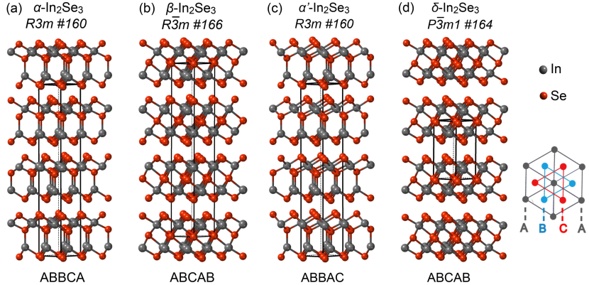
Although In2Se3 has been studied for many years, the reports on crystal structure are rather confusing and even contradictory in many cases Osamura et al. (1966); Popović et al. (1979); Ye et al. (1998), with remarkable disagreements on atomic positions within the layers and layer stacking sequence. At least four phases have been reported (, , , and ), with one of them being a 3D phase (labeled ) and the others identified as layered phases. The layered structures are composed of five atomic layer Se-In-Se-In-Se sets, with strong covalent bonds within each quintuple layer and van der Waals interactions connecting neighboring quintuple layers. Among the layered phases of In2Se3, and , shown in Fig. 1(a) and (b), are the most prominent, with a reported transition temperature of 473 K Ei-Shair and Bekheet (1992).
The reported values for the band gap of layered In2Se3, either from optical absorption spectra Marsillac et al. (2011); Ho and Wang (2013); Clavijo et al. (2009); Bodnar (2016) or calculated using first-principles methods based on the density functional theory Debbichi et al. (2015); Ji et al. (2013), vary from 0.55 eV to 1.5 eV, and the nature of the gap, i.e., direct or indirect, has often been overlooked. Here we perform hybrid functional calculations for the electronic and optical properties of four layered structures of In2Se3 (including the and structures shown in Fig. 1), paying special attention to the disparity between optical and fundamental band gaps. We compare the stability of the different phases through their formation enthalpies, calculate the real and imaginary parts of the dielectric functions, and determine optical absorption coefficients. We find that the layered structures all have indirect band gaps, with the lowest band gap of 0.17 eV and the highest of 1.35 eV. The calculated optical transition matrix elements reveal that the optical gap is significantly different from the fundamental band gap for two of the structures, and that the onset of optical absorption all occur at energies higher than 1 eV. We also compute the band alignment between the different phases, and find that the position of the conduction-band minimum (CBM) is relatively low with respect to the vacuum level, indicating a tendency for -type conductivity for all the layered In2Se3 structures.
II Computational approach
The calculations are based on the density functional theory Hohenberg and Kohn (1964); Kohn and Sham (1965) and the screened hybrid functional of Heyd-Scuseria-Ernzerhof (HSE06) Heyd et al. (2003, 2006) as implemented in the VASP code Kresse and Hafner (1993a, b). The interactions between the valence electrons and the ions are described using projector augmented wave (PAW) potentials Blöchl (1994); Kresse and Joubert (1999). To improve the description of the weak interaction between the quintuple layers of In2Se3, we adopted a van der Waals (vdW) correction according to DFT-D2 method of Grimme Grimme (2006). The structures were optimized using a cutoff of 320 eV for the plane wave basis set, until forces on the atoms were lower than 0.005 eV/Å. The Brillouin zone was sampled using a -centered 666 mesh of -points for the primitive cells.
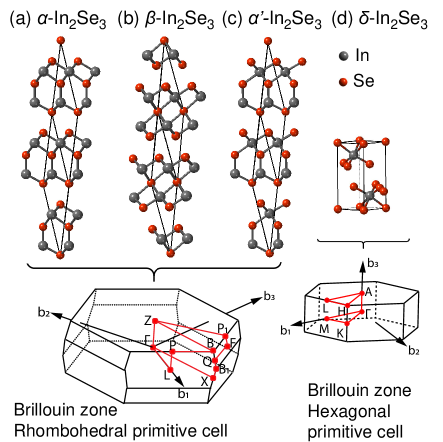
The structures of In2Se3 in Fig. 1(a)-(c) can be described by rhombohedral primitive cells containing one formula unit, while the structure in Fig. 1(d) is described by a hexagonal primitive cell with two formula units. These primitive cells are shown in Fig. 2. For the rhombohedral primitive cells we chose the following lattice vectorsFurthmüller and Bechstedt (2016):
| (1) |
where the three vectors have the same length , and form an angle defined by =. In practice, the lattice parameters of the layered structures of In2Se3 are often reported using conventional hexagonal unit cells. Our choice of lattice vectors for the rhombohedral primitive cells makes it easy to express the lattice parameters of the hexagonal unit cells, and in terms of and above. The lattice vectors of the hexagonal unit cells, containing three formula units, are given by:
| (2) |
The dielectric function along the in-plane direction () and out-of-plane direction () are written as:
| (3) |
where and are the diagonal and nondiagonal elements of the dielectric tensor obtained using the rhombohedral primitive cells with the lattice vectors given by Eq. 1 Furthmüller and Bechstedt (2016). The electronic band structures and dielectric functions were calculated using the HSE06 hybrid functional. Calculations using the GW method Hybertsen and Louie (1986); Shishkin and Kresse (2006) give band gaps that are systematically higher by only 0.1 eV. Contributions from excitons and phonon-assisted optical transitions to the absorption coefficient are expected to be relatively small and were not included in the present work.
III Results and discussion
III.1 Structure and stability of layered In2Se3
| (Å) | (Å) | Hf(eV) | |
| -In2Se3 | |||
| HSE06 | 4.066 | 30.368 | -3.982 |
| HSE06+vdW | 3.973 | 28.752 | -3.109 |
| Exp. | 4.00 | 28.80 Ye et al. (1998) | -2.858 Chatillon (1993) |
| 4.05 | 28.77 Osamura et al. (1966) | ||
| Previous calc. | 3.93 | 27.9 Debbichi et al. (2015) | |
| -In2Se3 | |||
| HSE06 | 3.978 | 29.890 | -3.737 |
| HSE+vdW | 3.904 | 27.671 | -3.071 |
| Exp. | 4.025 | 28.762 Lutz et al. (1988) | |
| 4.05 | 29.41Osamura et al. (1966) | ||
| Previous calc. | 4.00 | 29.04 Debbichi et al. (2015) | |
| -In2Se3 | |||
| HSE06 | 3.978 | 10.195 | -3.732 |
| HSE06+vdW | 3.902 | 9.322 | -3.042 |
| Exp. | 4.01 | 9.64 Popović et al. (1979) | |
| -In2Se3 | |||
| HSE06 | 4.003 | 30.279 | -3.975 |
| HSE06+vdW | 3.975 | 28.785 | -3.103 |
The crystal structures of layered In2Se3 are composed of sets of quintuple layers, Se-In-Se-In-Se, with each atomic layer containing only one elemental species arranged in a triangular lattice. Within the quintuple layers, the atoms form strong covalent/ionic bonds, while the interactions between neighboring quintuple layers are weak and of the van der Waals type. The crystal structures in Fig.1 differ in the stacking within the quintuple layer and inter quintuple layers. The most studied phases of layered In2Se3 are the and shown in Fig. 1(a) and (b). In the -In2Se3 structure, space group , the Se-In-Se-In-Se atomic layers are stacked in the ABBCA sequence, where one of the In is fourfold coordinated in a tetrahedral environment, and the other is sixfold coordinated in an octahedral environment. In the -In2Se3, space group , both In atoms are sixfold coordinated in octahedral environments. In a variant of the -In2Se3 structure, here labeled , space group , the Se-In-Se-In-Se atomic layers are stacked in the ABBAC sequence, where one of the In is fourfold coordinated, and the other is sixfold coordinated, as shown in Fig. 1(c). The -In2Se3 structure, space group , is a variant of the -In2Se3, differing only in the stacking of the quintuple layers. While in -In2Se3, each period along the out-of-plane direction ( axis) contains three quintuple layers [Fig. 1(b)], in -In2Se3, each period along axis contains only one quintuple layer, as shown in Fig. 2(d).
The calculated lattice parameters of , , , and -In2Se3, using both HSE06 and HSE06 with van der Waals correction (HSE06+vdW) are listed in Table 1. HSE06 leads to a good agreement between theoretical and experimental results for in-plane lattice parameters , however the error in the out-of-plane lattice parameter exceeds compared to the experimental value for the structure. HSE06+vdW improves the description of , reducing the error to less than .
The calculated formation enthalpies are also listed in Table 1. is defined as:
| (4) |
where ) are the total energies per formula unit of In2Se3 in the different crystal structures, and are the total energies per atom of In and Se bulk phases. Using HSE06+vdW, we find that -In2Se3 has the lowest formation enthalpy (-3.109 eV), followed by , , and -In2Se3. The calculated formation enthalpy of -In2Se3 is in good agreement with available experimental data Chatillon (1993). We note that vdW corrections systematically increase formation enthalpies by about 0.8 eV for the different phases of layered In2Se3.
III.2 Electronic structure of layered In2Se3
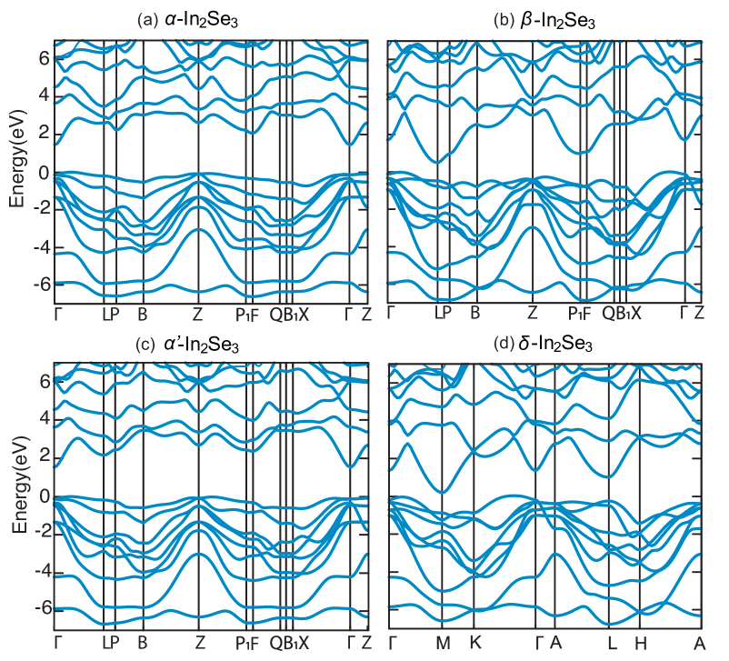
The calculated band structures of , , , and -In2Se3, using the primitive cells, are shown in Fig. 3, including all the high symmetry points in the irreducible part of the Brillouin zone. The four layered phases of In2Se3 display fundamental indirect band gaps, with highly dispersive conduction bands (small effective electron masses) derived from In orbitals, and much less dispersive valence bands derived mostly from Se orbitals.
For -In2Se3, the valence-band maximum (VBM) occurs along the -L direction (about one third of the -L distance from ), while the conduction-band minimum (CBM) is located at , with an indirect band gap of 1.34 eV. The direct gap at is 1.46 eV. For -In2Se3, the VBM occurs along the -X direction (about one third of the distance from ), while the CBM is located at the L point, with an indirect band gap of 0.49 eV. The conduction-band edge at is 1.21 eV higher than at L, and the valence-band edge at is 0.12 eV lower than the VBM along -X, so that the direct gap at is 1.82 eV. The phase has a very similar band structure as the -In2Se3, with a band gap of 1.35 eV, i.e., only 0.01 eV higher than that of -In2Se3. The -In2Se3 has a small band gap of only 0.17 eV, with the VBM along the -K direction and the CBM at the M point in the hexagonal Brillouin zone [Fig. 2(d)]. The direct gap at is 1.55 eV.
Previous results of first-principles calculations for the band gap of In2Se3 vary in a wide rangeDebbichi et al. (2015); Ji et al. (2013). The few reported band structures for bulk In2Se3 are nevertheless incomplete for the following reasons. First, the calculations were performed using the hexagonal unit cells, instead of the primitive cells. This may prevent a proper analysis of the direct versus indirect nature of the band gap since the Brillouin zone of the hexagonal unit cell is folded into that of the rhombohedral primitive cell. A direct gap in the Brillouin zone of the hexagonal cell may well involve distinct points in the Brillouin zone of the primitive rhombohedral cell. Second, and more worrisome, the calculations for the hexagonal unit cells do not include all high-symmetry points in the irreducible part of the Brillouin zone; they only include paths in the in-plane direction passing through the point. In fact, our calculations for the band structure of -In2Se3 using the hexagonal unit cell show that while the VBM occurs at the -K direction, the CBM occurs at the L point, i.e., not located in paths in the in-plane direction passing through the point [see the Brillouin zone in Fig. 2(d) for reference].
Based on full-potential linearized augmented plane-wave and local orbitals (FPLAPW+lo) basis method and the modified Becke Johnson (mBJ) meta-GGA, an indirect band gap of 0.55 eV and a direct band gap at of 1.5 eV were reported for -In2Se3Ji et al. (2013). The authors argued that the calculated band gap was underestimated due to DFT band gap problem. However, the Becke Johnson (mBJ) meta-GGA approximation was designed to overcome this problem and to give band gaps in close agreement with experimental values. DFT-GGA calculations for and -In2Se3 resulted in indirect band gaps of 0.49 eV and 0.21 eV, while using the GW method, gaps of 1.25 eV and 0.7 eV were obtainedDebbichi et al. (2015). However, the authors calculated the band structures using the hexagonal unit cells and only considered in-plane -paths passing through the point.
We also calculated the optical transition matrix elements between valence- and conduction-band states for the four layered structures of In2Se3. For the and ’ structures, we find the transition at to be allowed and slightly higher in energy than the fundamental indirect band gap. For -In2Se3, we find that the lowest energy direct transition at L is not allowed and that the optical gap originates from the second valence band to the conduction band at L. For -In2Se3, the optical gap is associated with the transition from the first valence band and conduction band at M. These results show a disparity between the fundamental and the optical gaps, which are larger than 1 eV in the case of and -In2Se3.
III.3 Dielectric functions and absorption coefficients of layered In2Se3
The optical properties of layered In2Se3 are discussed based on the real and imaginary parts of the dielectric matrix, absorption coefficient and the optical transition matrix elements. To determine the optical band gap from the dielectric functions and the derived absorption coefficient we employed the tetrahedral method for the integration over the Brillouin zone, with a small Lorentzian broadening parameter of 0.001 eV. The calculations for the dielectric function were carried out for the rhombohedral primitive cells for , , and -In2Se3, and then converted to the hexagonal directions according to Eq. 3.
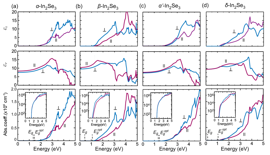
The real and imaginary parts of the dielectric function are shown in Fig. 4. Due to the hexagonal layered structure, we expect the dielectric function to be anisotropic, with nonzero components only in the out-of-plane () and in the in-plane () directions.
For , , and -In2Se3, the real part of the dielectric tensor at zero energy (or frequency), is higher in the in-plane than in the out-of-plane direction, i.e., . This is expected since the electronic screening is stronger in the in-plane directions than in the out-of-plane direction due to the layered nature of the crystal structure. For the phase, we find , likely due to the alignment of the Se atoms connecting two neighboring quintuple layers, that favors the overlap of Se orbitals across the quintuple layers, and the smaller distance between the quintuple layers.
The absorption coefficients were determined from the real and imaginary parts of the dielectric matrix and are shown at the bottom panel in Fig. 4. For all the structures investigated, the amplitude of absorption coefficients are rather large for above band-gap excitations, i. e., exceeding 106 cm-1, which are of the same order of magnitude as that in direct gap III-V semiconductors Stillman et al. (1984). The optical absorption coefficients start increasing only at energies higher than 1 eV. Note that the optical band gap of and -In2Se3 are similar to the fundamental band gap, because the small difference between the VBM and the of valence band edge at -point. In contrast, the optical band gap of 1.27 eV for -In2Se3 and 1.11 eV for -In2Se3 are much higher than the fundamental gap of 0.49 eV and 0.17 eV, respectively.
Optical absorption measurements of and -In2Se3 single crystals, where the form was obtained by heating -In2Se3 crystals above 473 K in a furnace, revealed optical band gaps of 1.356 eV and 1.308 eV respectivelyJulien et al. (1990). Optical transmission measurements in -In2Se3 films, deposited using thermal evaporation on glass substrates, indicated an indirect fundamental band gap slightly below the optical band gap of 1.37 eV El-Shair and Bekheet (1992). Layered In2Se3 samples grown by vapor phase techniqueYe et al. (1998) have shown onset in the absorption spectra at 1.26 eV, with an estimated fundamental indirect gap of about 1.1 eV. The authors proposed a structure composed of quintuple layers with an unlikey truncated wurtzite crystal arrangement within each quintuple layer, where one Se atoms at the boundary is one-fold coordinated. We believe these results actually refer to -In2Se3 based on the reported lattice parameters. Films of -In2Se3 fabricated by ion-beam sputtering at 312 K from single crystals showed a band gap of 1.58 eV, determined from transmittance spectra Bodnar (2016). More recently, a band gap of 1.46 eV for -In2Se3 and 1.38 eV for -In2Se3 were determined using photocurrent spectroscopyWang et al. (2017). The authors noted that the -In2Se3 films (86 nm) were highly electrically conductive as a metal. All these results indicate optical band gaps above 1 eV, in agreement with our calculations.
Our calculations also offer some insights on the electronic structure of (InxBi1-x)2Se3 even though we did not carry out explict calculations for this system. Recent experiments have proposed that adding In to Bi2Se3 increases the band gap and reduces the Fermi level which is resonant in the conduction band of Bi2Se3, leading to a transition from a doped topological insulator to a trivial insulator with band gap over 1 eV Liu and Vanderbilt (2013). However, it is unclear if the conduction-band edge in the (InxBi1-x)2Se3 alloy is pushed up or if the ARPES measurements do not capture the range where the band edges occur Brahlek et al. (2012); Wu et al. (2013); Liu and Vanderbilt (2013). From our results, it is unlikely that alloying -In2Se3 (band gap 0f 0.49 eV) with Bi2Se3 (0.22 eV) Martinez et al. (2017) would lead to fundamental band gaps larger than 1 eV as previously proposed Liu and Vanderbilt (2013).
III.4 Band alignments
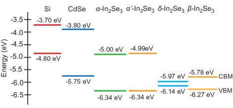
Finally, we calculated the band alignment between the different structures of layered In2Se3. To be able to directly compare the VBM and CBM of the different phases, we fixed the volume per formula unit in each calculation to be that in -In2Se3, so that the average electrostatic potential, which is used as reference in the HSE06 calculations, is the same for the different structures. In order to align with the vacuum level, we used a slab of -In2Se3 with 9 quintuple layers and determined the averaged electrostatic potential of the middle quintuple layer with respect to the potential in the vacuum region of the slab. The results are shown in Fig. 5 and are compared to the values of the VBM and CBM for CdSe and Si from the literature Van de Walle and Neugebauer (2003).
From Fig. 5, we note that the CBM of layered In2Se3 are significantly lower than that of CdSe or Si, and lower than the standard hydrogen electrode potential (i.e., -4.5 eV below the vacuum level Van de Walle and Neugebauer (2003)), implying that all the layered phases of In2Se3 will have a tendency for -type conductivity. This is specially the case of -In2Se3 and -In2Se3. This explains the recent measurements of photocurrent spectroscopy Wang et al. (2017) where -In2Se3 was reported to behave as a metal. It is also likely that the band gap of 1.38 eV determined from the onset in the photocurrent spectrum is larger than the calculated optical gap of 1.23 eV in the present work due to the high density of electrons in the conduction band in the experiment, leading to a blue shift due to the MossBurstein effect.
The VBM of the layered In2Se3 phases are all lower than that of CdSe. This can be explained by the - coupling in CdSe which is likely to be stronger than in In2Se3. In CdSe, the filled Cd 4 is well below the valence band composed of Se 5 orbitals. The Cd 4 states have the same symmetry as the VBM states, so the - coupling pushes the VBM upwards. Since In 4 is lower than the Cd 4, the - coupling is expected to be weaker in In2Se3, resulting in lower VBM.
IV Summary
We reported on the electronic structure and optical properties of layered In2Se3 using the HSE06 hybrid functional with vdW corrections. We found that the fundamental band gaps are indirect, and the optical gaps are all larger than 1 eV. In the case of -In2Se3, which shares the same crystal structure of Bi2Se3, the fundamental band gap is only 0.49 eV, while the optical gap is 1.27 eV. The small fundamental band gap of -In2Se3 is not expected to lead to alloys of In2Se3 and Bi2Se3 with gaps much larger than the gaps of the parent compounds as suggested in the literature. The calculated absorption coefficient are found to exceed 106 cm-1 and the onsets of optical absorption are overall in good agreement with experimental observations.
Acknowledgments
We thank S. Law and Y. Wang for fruitful discussions. This work was supported by the National Science Foundation Faculty Early Career Development Program DMR-1652994. This research was also supported by the the Extreme Science and Engineering Discovery Environment supercomputer facility, National Science Foundation grant number ACI-1053575, and the Information Technologies (IT) resources at the University of Delaware, specifically the high performance computing resources.
References
- Choi et al. (2017) W. Choi, N. Choudhary, G. H. Han, J. Park, D. Akinwande, and Y. H. Lee, Materials Today 20, 116 (2017), 1403.4270 .
- Yang et al. (2016) S. Yang, C. Wang, C. Ataca, Y. Li, H. Chen, H. Cai, A. Suslu, J. C. Grossman, C. Jiang, Q. Liu, and S. Tongay, ACS Applied Materials and Interfaces 8, 2533 (2016).
- Zheng et al. (2016) Z. Zheng, T. Zhang, J. Yao, Y. Zhang, J. Xu, and G. Yang, Nanotechnology 27, 225501 (2016).
- Zhang et al. (2009) H. Zhang, C.-X. Liu, X.-L. Qi, X. Dai, Z. Fang, and S.-C. Zhang, Nature Physics 5, 438 (2009).
- Padilha et al. (2014) J. E. Padilha, H. Peelaers, A. Janotti, and C. G. Van De Walle, Physical Review B 90, 1 (2014).
- Peng et al. (2007) H. Peng, D. T. Schoen, S. Meister, X. F. Zhang, and Y. Cui, Journal of the American Chemical Society 129, 34 (2007).
- Balakrishnan et al. (2016) N. Balakrishnan, C. R. Staddon, E. F. Smith, J. Stec, D. Gay, G. W. Mudd, O. Makarovsky, Z. R. Kudrynskyi, Z. D. Kovalyuk, L. Eaves, and A. Patanè, 2D Materials 3, 1 (2016).
- Zhai et al. (2010) T. Zhai, X. Fang, M. Liao, X. Xu, L. Li, B. Liu, and Y. Koide, ACS Nano 4, 1596 (2010).
- Jacobs-Gedrim et al. (2014) R. B. Jacobs-Gedrim, M. Shanmugam, N. Jain, C. A. Durcan, M. T. Murphy, T. M. Murray, R. J. Matyi, R. L. Moore, and B. Yu, ACS Nano 8 (2014).
- Island et al. (2015) J. O. Island, S. I. Blanter, M. Buscema, H. S. Van Der Zant, and A. Castellanos-Gomez, Nano Letters 15, 7853 (2015).
- Lee et al. (2005) H. Lee, D.-H. Kang, and L. Tran, Materials Science and Engineering: B 119, 196 (2005).
- Yu et al. (2007) B. Yu, S. Ju, X. Sun, G. Ng, T. D. Nguyen, M. Meyyappan, and D. B. Janes, Applied Physics Letters 91, 133119 (2007).
- Zheng et al. (2015) W. Zheng, T. Xie, Y. Zhou, Y. L. Chen, W. Jiang, S. Zhao, J. Wu, Y. Jing, Y. Wu, G. Chen, Y. Guo, J. Yin, S. Huang, H. Q. Xu, Z. Liu, and H. Peng, Nature communications 6, 1 (2015).
- Ding et al. (2017) W. Ding, J. Zhu, Z. Wang, Y. Gao, D. Xiao, Y. Gu, Z. Zhang, and W. Zhu, Nature Communications 8, 14956 (2017).
- Osamura et al. (1966) K. Osamura, Y. Murakami, and Y. Tomiie, Journal of the Physical Society of Japan 21, 1848 (1966).
- Popović et al. (1979) S. Popović, A. Tonejc, B. Gržeta-Plenković, B. Čelustka, and R. Trojko, Journal of Applied Crystallography 12, 416 (1979).
- Ye et al. (1998) J. Ye, S. Soeda, Y. Nakamura, and O. Nittono, Japanese Journal of Applied Physics 37, 4264 (1998).
- Ei-Shair and Bekheet (1992) H. T. Ei-Shair and A. E. Bekheet, Journal of Physics D: Applied Physics 25, 1122 (1992).
- Marsillac et al. (2011) S. Marsillac, N. S. Mangale, V. Gade, and S. V. Khare, Thin Solid Films 519, 5679 (2011).
- Ho and Wang (2013) C.-H. Ho and Y.-P. Wang, Optical Materials Express 3, 1420 (2013).
- Clavijo et al. (2009) J. Clavijo, E. Romero, , and G. Gordillo, Journal of Physics: Conference Series 167, 12016 (2009).
- Bodnar (2016) I. V. Bodnar, Semiconductors 50, 715 (2016).
- Debbichi et al. (2015) L. Debbichi, O. Eriksson, and S. Lebegue, Journal of Physical Chemistry Lettrs 6, 3098 (2015).
- Ji et al. (2013) H. Ji, A. Reijnders, T. Liang, L. M. Schoop, K. S. Burch, N. P. Ong, and R. J. Cava, Materials research bulletin 48, 2517 (2013).
- Hohenberg and Kohn (1964) P. Hohenberg and W. Kohn, Physical Review 136, B864 (1964).
- Kohn and Sham (1965) W. Kohn and L. J. Sham, Physical Review 140, A1133 (1965).
- Heyd et al. (2003) J. Heyd, G. E. Scuseria, and M. Ernzerhof, Journal of Chemical Physics 118, 8207 (2003).
- Heyd et al. (2006) J. Heyd, G. E. Scuseria, and M. Ernzerhof, Journal of Chemical Physics 124 (2006).
- Kresse and Hafner (1993a) G. Kresse and J. Hafner, Physical Review B 47, 558 (1993a).
- Kresse and Hafner (1993b) G. Kresse and J. Hafner, Physical Review B 48, 13115 (1993b).
- Blöchl (1994) P. E. Blöchl, Physical Review B 50, 17953 (1994).
- Kresse and Joubert (1999) G. Kresse and D. Joubert, Physical Review B 59, 1758 (1999).
- Grimme (2006) S. Grimme, Journal of Computational Chemistry 27, 1787 (2006).
- Furthmüller and Bechstedt (2016) J. Furthmüller and F. Bechstedt, Physical Review B 93, 115204 (2016).
- Hybertsen and Louie (1986) M. S. Hybertsen and S. G. Louie, Phys. Rev. B 34, 5390 (1986).
- Shishkin and Kresse (2006) M. Shishkin and G. Kresse, Physical Review B 74, 035101 (2006).
- Chatillon (1993) C. Chatillon, Journal of Crystal Growth 129, 297 (1993).
- Lutz et al. (1988) H. D. Lutz, M. Fischer, H. P. Baldus, and R. Blachnik, Journal of The Less-Common Metals 143, 83 (1988).
- Stillman et al. (1984) G. Stillman, V. Robbins, and N. Tabatabaie, IEEE Transactions on Electron Devices 31, 1643 (1984).
- Julien et al. (1990) C. Julien, A. Chlwy, and D. Siapkas, Physica Status Solidi (a) 553 (1990).
- El-Shair and Bekheet (1992) H. T. El-Shair and A. E. Bekheet, Journal of Physics D: Applied Physics 25, 1122 (1992).
- Wang et al. (2017) Q. Wang, L. Yang, S. Zhou, X. Ye, Z. Wang, W. Zhu, M. D. McCluskey, and Y. Gu, The Journal of Physical Chemistry Letters 8, 2887 (2017).
- Liu and Vanderbilt (2013) J. Liu and D. Vanderbilt, Physical Review B 88, 224202 (2013).
- Brahlek et al. (2012) M. Brahlek, N. Bansal, N. Koirala, S. Y. Xu, M. Neupane, C. Liu, M. Z. Hasan, and S. Oh, Physical Review Letters 109, 1 (2012).
- Wu et al. (2013) L. Wu, M. Brahlek, R. V. Aguilar, A. V. Stier, C. M. Morris, Y. Lubashevsky, L. S. Bilbro, N. Bansal, S. Oh, and N. P. Armitage, Nature Physics 9, 410 (2013).
- Martinez et al. (2017) G. Martinez, B. A. Piot, M. Hakl, M. Potemski, Y. S. Hor, A. Materna, S. G. Strzelecka, A. Hruban, O. Caha, J. Novák, A. Dubroka, Č. Drašar, and M. Orlita, Scientific Reports 7, 6891 (2017).
- Van de Walle and Neugebauer (2003) C. G. Van de Walle and J. Neugebauer, Nature 423, 626 (2003).