Suppression of Charge Density Wave by Substrate Induced Doping on TiSe2/TiO2 Heterostructure
Abstract
Substrate engineering provides an opportunity to modulate the physical properties of quantum materials in thin film form. Here we report that TiSe2 thin films grown on TiO2 have unexpectedly large electron doping that suppresses the charge density wave (CDW) order. This is dramatically different from either bulk single crystal TiSe2 or TiSe2 thin films on graphene. The epitaxial TiSe2 thin films can be prepared on TiO2 via molecular beam epitaxy (MBE) in two ways: by conventional co-deposition using selenium and titanium sources, and by evaporating only selenium on reconstructed TiO2 surfaces. Both growth methods yield atomically flat thin films with similar physical properties. The electron doping and subsequent suppression of CDW order can be explained by selenium vacancies in the TiSe2 film, which naturally occur when TiO2 substrates are used. This is due to the stronger interfacial bonding that changes the ideal growth conditions. Our finding provides a way to tune the chemical potential of chalcogenide thin films via substrate selection and engineering.
keywords:
TiSe2, charge transfer, substrate engineering, suppression of CDWGeballe Laboratory for Advanced Materials, Departments of Physics and Applied Physics, Stanford University, Stanford, California 94305, USA \altaffiliationThese two authors contributed equally to this work. \alsoaffiliationGeballe Laboratory for Advanced Materials, Departments of Physics and Applied Physics, Stanford University, Stanford, California 94305, USA \altaffiliationThese two authors contributed equally to this work. \alsoaffiliationGeballe Laboratory for Advanced Materials, Departments of Physics and Applied Physics, Stanford University, Stanford, California 94305, USA \alsoaffiliationGeballe Laboratory for Advanced Materials, Departments of Physics and Applied Physics, Stanford University, Stanford, California 94305, USA
1 Introduction
Thin film growth using MBE has been shown to be a powerful tool for studies of correlated materials1, 2, 3. Physical properties of correlated thin films can be significantly changed through substrate selection and engineering. For instance, titanate substrates including SrTiO3, anatase and rutile TiO2 have been found to have multiple effects on FeSe films, including large and anisotropic strain, charge transfer, interfacial electron-phonon coupling and superconducting transition temperature enhancement2, 4, 5, 6. It is therefore interesting to test the effect of titanate substrates on other thin films of correlated electron systems.
Layered transition-metal dichalchogenides (TMDC) have been extensively studied due to their interesting physical properties, including the emergence of superconductivity and CDW order7, 8. Specifically, TiSe2 has attracted significant interest due to the controversy over the driving force of its CDW order. TiSe2 bulk single crystals undergo a phase transition at around 200 K into a CDW state characterized by the 3D commensurate () wave vector 9. There are multiple explanations of the origin of the CDW in TiSe2, including band Jahn-Teller effect10, exciton condensation 11, 12 and conventional Fermi-surface nesting13. Monolayer thin films of TiSe2 have been grown on bilayer graphene using MBE, yielding similar band structure, and CDW with a 2D commensurate () wave vector. The CDW transition temperature for monolayer TiSe2 on graphene is slightly higher than that of bulk crystals 14, 15. In multilayer thin films of TiSe2 on graphene, the CDW wave vector changes from 2D-like to 3D-like and the transition temperature decreases to bulk value as thickness increases16. The intriguing physical properties of TiSe2 make it an attractive testbed for the study of substrate effects on thin films.
In this work, we grew TiSe2 on rutile TiO2 (100) (TiSe2/TiO2) and bi-layer graphene (TiSe2/graphene) substrates using MBE and characterized its electronic structure via angle-resolved photoemission spectroscopy (ARPES). We find that the TiSe2 films on TiO2 (TiSe2/TiO2) are heavily electron doped and do not show the signatures of a CDW in ARPES spectra. Furthermore, after depositing selenium on vacuum-annealed TiO2 substrates (thereafter noted as Se:TiO2), Se atoms reacts with the reconstructed substrate surface, and organizes into epitaxial films of TiSe2. Our experiments on TiSe2/TiO2 films provide a way to tune the chemical potential and change the ground state property of thin films through substrate engineering.
2 Electronic Band Structure
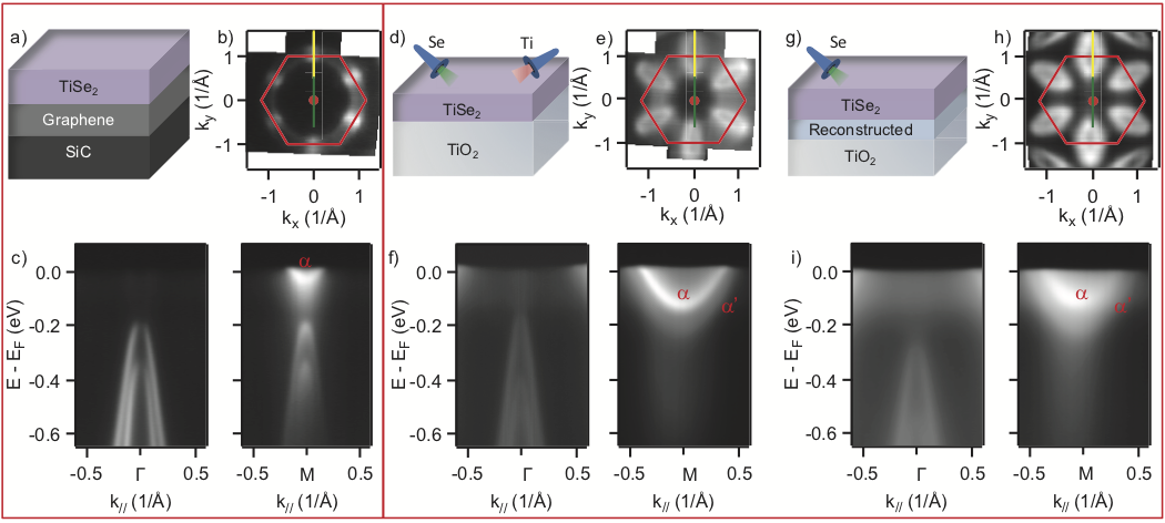
Previous researchers have reported the band structure of TiSe2 (either in bulk form or TiSe2/graphene)17, 14, and the results of TiSe2 bulk single crystals and TiSe2/graphene are very similar. Near the Fermi level (), there is a pair of bands centered at the point. At the M point, the bottom of an electron band reaches just below . We measured the Fermi surface and band structure of TiSe2/graphene at 20 K, shown in Fig 1(b, c). At this measurement temperature, TiSe2/graphene is in the CDW phase and the ARPES data clearly show that the hole bands at are folded to M. There is little signal of the folding from the electron band at M to , which is consistent with previous ARPES works17, 14. From the Fermi surface map we observe six tiny pockets formed by electron bands at M. These results are consistent with the previous research on TiSe2/graphene14, 15, 16.
The Fermi surface and band structure of TiSe2/TiO2 at the same measurement temperature of 20 K, shown in Fig 1(e-f), exhibit a few stark differences from those of TiSe2/graphene. The bands are no longer folded, indicating the lack of CDW order. Also the electron pockets are much larger for TiSe2/TiO2, representing a doping of electron per unit cell, calculated from the Fermi surface volume. In contrast, TiSe2/graphene has a doping of merely over the perfectly stoichiometric compound (see Fig 1(b)). The doping of TiSe2/graphene is nonzero possibly due to Se vacancies. Besides those two features, below the main electron band near the M point (denoted as in Fig. 1(f)) there is a weaker copy of the band around 100 meV below the main band and crossing the Fermi level, denoted as band. This “copy” band is more clearly seen in the second energy derivative of the ARPES spectra in Supplemental Figure 2. This cannot be attributed to the quantum well effects in the finite-thickness films, as the energy difference between and is thickness independent up to 24 monolayers (ML) (see Supplemental Fig. 1). Further work needs to be done to explain the origin of the band .
All the three features mentioned above, including lack of CDW, large electron doping and the “copy” band at M, have little thickness dependence from 3ML to 24ML, as is demonstrated in Supplemental Fig. 1.
Rutile TiO2 (100) surface undergoes a (3 1) reconstruction above 670 ∘C. During this process parts of surface atoms are lost, leading to a terraced surface with exposed atoms of titanium 18. Surprisingly, after annealing the rutile TiO2 substrate above the surface reconstruction temperature in vacuum, we can grow epitaxial thin films of TiSe2 by only depositing Se. Given that, we speculate that Se atoms react with the Ti atoms exposed to vacuum due to the reconstruction, and form TiSe2 (denoted before as Se:TiO2). The electronic band structure of Se:TiO2, shown in Fig 1(i), is very similar to that of TiSe2/TiO2 grown by co-deposition of Se and Ti. As in TiSe2/TiO2, there is no band folding between and M, which indicates the suppression of CDW, and very large electron doping level of electron/unit cell. Also below the main band near M there is a “copy” band , shown in Fig. 1(i), similar to the case of TiSe2/TiO2.
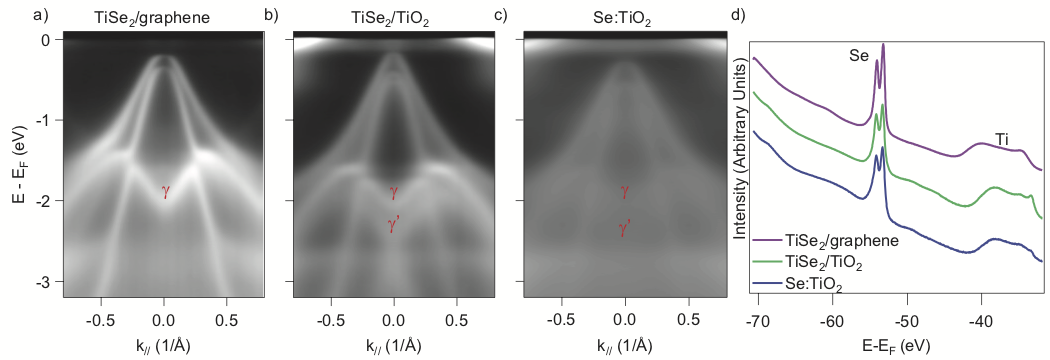
We further compared the band structure of TiSe2/graphene and the TiSe2 films grown on TiO2. Figure 2 (a-c) display the deeper valence bands for 1ML TiSe2/graphene, 6ML TiSe2/TiO2 and Se:TiO2, respectively. In TiSe2/TiO2, there are two bands which share similar dispersion but are separated by 350 meV. There is a hint of the band in Se:TiO2 as well, but the signal is much weaker. The origin of the band in TiSe2 films on TiO2 substrate needs further work to elucidate. Besides this difference, the vast majority of band features are similar with the exception of a chemical potential shift in the cases of TiSe2/TiO2 and Se:TiO2.
Figure 2 (d) shows the core level spectra of TiSe2/graphene, 7ML TiSe2/TiO2 and Se:TiO2. The Se double peaks are similar for all three systems in both position and magnitude. The Ti peaks for TiSe2/TiO2 and Se:TiO2 are shifted towards lower binding energy and have slightly different shapes. Previous reports discuss the creation of Ti3+ states on the surface of vacuum annealed TiO219, which will cause additional shoulders with lower binding energy in the Ti X-ray photoemission spectra. Thus we may explain the energy shift in the core level spectra of TiSe2/TiO2 and Se:TiO2 by the formation of Ti3+ states. However, this energy shift is also seen for 7ML TiSe2/TiO2, where the signal from the Ti3+ ions in TiO2 substrate should diminish. With an estimated probing depth of 0.6 nm 20, the Ti3+ signature from TiO2 should diminish by a factor of 1,000 for a 7ML film compared to the bare TiO2 substrate. This is in contradiction to the observation that Se:TiO2 and TiSe2/TiO2 have similar Ti photoemission spectra. Such an observation suggests that the electron doping on TiSe2/TiO2 may induce Ti3+ ions in TiSe2 films as well. The measurement of deeper valence band and core level further verifies that the films on TiO2, grown by either Se deposition or Ti/Se co-deposition, are TiSe2.
3 Surface Characterization
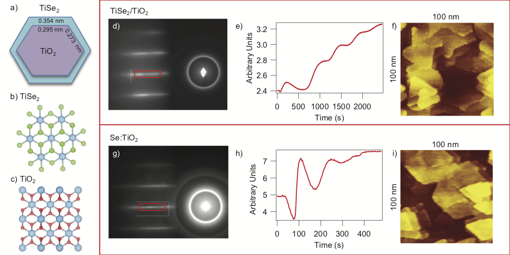
Next we continue to characterize the quality of the TiSe2 films on TiO2. TiSe2 is a layered material with hexagonal lattice and a lattice constant of nm. TiO2 (100) surface is rectangular with lattice parameters nm, nm. We can view the (100) surface of the substrate as a distorted hexagonal lattice, but this still leads to a large and anisotropic strain of more than 20%, as is shown in Figure 3(a). Therefore, it seems unlikely to achieve layer-by-layer growth of TiSe2/TiO2. Nonetheless, Reflective High Energy Electron Diffraction (RHEED) and Scanning Tunneling Microscope (STM) topography show epitaxial growth of TiSe2 for both TiSe2/TiO2 and Se:TiO2. The strain is 2% determined by RHEED diffraction pattern. The RHEED images, oscillations of RHEED intensity and STM topography are shown in Figure 3(d-i). Intriguingly, we can see RHEED intensity “oscillations” for Se:TiO2, even though the reaction is between deposited Se atoms and Ti atoms on the substrate. These results, combined with the clarity in the ARPES spectra, demonstrate the excellent surface quality of the film for both Se deposition and co-deposition.
4 Analysis
With the chemical composition and surface quality verified for TiSe2/TiO2 and Se:TiO2, we now turn back to the explanation of their electronic band structures. The two main features of TiSe2 films on TiO2 are the large electron doping and the suppression of the CDW.
Currently the origin of the CDW in TiSe2 is still under debate. Some attribute it to a Peierls charge density wave, which is created by a spontaneous crystal distortion driven by the electron-phonon interaction9, 13. Many others describe the low-temperature phase as excitonic condensation where electrons and holes combine into excitons which then Bose condense11, 12. In either case, it is expected that external electron doping will suppress the CDW. For the case of a Peierls CDW, increasing carrier density will alter the Fermi surface nesting conditions and promote superconductivity, which competes with the CDW. For an excitonic condensate, doping will break the balance between electrons and holes and hence restraining the condensation. Previous researchers have doped TiSe2 by Cu intercalation 21, 22 and ionic liquid gating 23, and both methods lead to the destruction of the CDW and the formation of a superconductivity dome in the phase diagram.
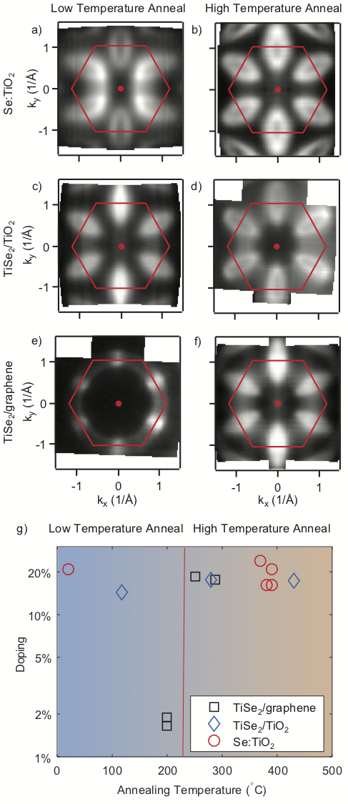
The most unusual aspect of this system is the magnitude of its doping. Changing post-growth annealing temperature of TiSe2 can control Se vacancy defects, which may act as electron dopants24. By default we do post-growth annealing at the growth temperature, which is 200 ∘C for TiSe2/graphene, and 360-380 ∘C for TiSe2/TiO2. Therefore, we systematically compare the films of all 3 growth modes with different post-growth annealing temperatures to investigate its effect on the electronic properties. Figure 4(e-f) shows the Fermi surface of TiSe2/graphene after low and high temperature post-growth annealing. The Fermi surface becomes significantly larger after a mere 50∘C increase in annealing temperature (from 200 ∘C to 250 ∘C), indicating that the high temperature post-growth annealing can create Se vacancies and induce electron doping. Nevertheless, if we immediately quench TiSe2/TiO2 and Se:TiO2 films to temperatures below 200 ∘C after growth, the Fermi surface volume is still much larger than the case of TiSe2/graphene, which is clear if we compare Fig. 4(a, c, e). When the doping level is higher than 0.15 electron/Ti atom, as shown in Fig 4 (a-d,f), the CDW order is destroyed. This shows that TiO2 substrate, directly or indirectly, induces large doping level into TiSe2.
It is plausible to assume the interfacial charge transfer from work function difference as the origin of the electron doping in TiSe2 films on TiO2. The work function difference between TiSe225 and TiO226 is as large as 1.2 eV, which may enable direct interfacial transfer of electrons from TiO2 substrate to TiSe2 film. However, the effects of interfacial charge transfer are strongly limited by the thickness of films due to electronic screening from the films. Since there is no thickness dependence of the Fermi surface size up to 24ML (see Supplemental Fig. 1), the work function induced interfacial charge transfer cannot be the main reason for the electron doping for TiSe2 films on TiO2.
Below we consider an indirect effect from the TiO2 substrate: the strong interfacial bonding between TiSe2 and TiO2 leads to a growth window with higher growth temperature. More Se vacancies are created during growth under this condition compared to the case of TiSe2/graphene, resulting in electron doping and suppression of CDW in TiSe2.
The ideal growth temperature for TiSe2/TiO2 and Se:TiO2 is consistently higher than that for TiSe2/graphene. The ideal growth temperature for TiSe2/TiO2 and Se:TiO2 is between 350-380 ∘C, below which the growth yields amorphous films. On the other hand, if we grow TiSe2/graphene at any temperature above 250 ∘C, there will be no formation of new RHEED streaks. This means that at this temperature, the Se re-evaporation rate is to high to allow the growth of TiSe2 on graphene. This substrate-induced growth temperature difference between graphene and TiO2 can be explained by the growth dynamics. Graphene provides much weaker interfacial interaction, therefore the ideal growth temperature is low. In contrast, TiO2 surface tends to form stronger bonds with TiSe2 on the interface, thus a higher growth temperature is needed to provide sufficient diffusion rate necessary to form pristine films.
At the growth temperature of TiSe2/TiO2 and Se:TiO2 (380 ∘C), Se re-evaporation can be very strong, according to the results of TiSe2/graphene from both Fig 4(f) and a previous STM study 24. As a result, during the growth process, there is already strong Se re-evaporation, leading to Se deficiency and electron doping, even though we are growing in a Se-rich regime. However, the heavily doped TiSe2/TiO2 and Se:TiO2 films generally show superior ARPES spectrum than the TiSe2/graphene films with higher post-growth annealing temperatures. The sharper ARPES is indicative of improved crystalline quality. Thus the enhanced substrate-film bonding yields significant selenium defects and therefore large electron doping, while maintaining superior crystallinity overall.
To summarize, we can explain the suppression of charge density wave order by the large electron doping, and explain the electron doping by Se vacancies created by substrate induced change of growth conditions. The doping is because of the change of growth condition instead of a direct effect of substrate, which can explain why this effect is independent of film thickness up to 24ML.
5 Conclusion
We grew TiSe2 on rutile TiO2 (100) substrates using MBE, in which substrate effects provide large doping to TiSe2 that suppresses CDW order. This demonstrates that, in the course of tuning the chemical potential of thin film samples, we can add a large and flexible offset by selecting and engineering the substrate. The substrate-induced doping, compared to conventional methods including alkali metal atom intercalation and ionic liquid gating, provides a cleaner way of doping thin films in that it does not provide external impurities to the system. In addition, our results demonstrate that pristine TiSe2 thin films can form on reconstructed TiO2 substrate after Se deposition, which may pave the way to new growth methods of other chalcogenide/oxide heterostructure, and improve our understanding of the chemical property of the reconstructed surface of oxides.
Previous studies doped electrons into TiSe2 to a maximal level of 0.06 electron per unit cell, and observed superconductivity21, 22, 27. In contrast, TiSe2 films on TiO2 reported in this work has a doping of 0.16 electron per unit cell without any external intercalation or liquid gating, entering into an unexplored regime in the TiSe2 phase diagram. It would be interesting to do further experiments to investigate into the transport properties of TiSe2 films on TiO2. We also plan to apply similar substrate engineering methods to other heterostructures of correlated materials as a powerful way to explore further in the phase diagrams.
Methods
Growth
For TiSe2/TiO2, Shinkosha STEP TiO2 (100) substrates were mounted on a molybdenum sample holder with silver paste and placed into an MBE chamber. The base pressure of the MBE chamber was 8 torr. Substrates were then degassed at 450 - 650 ∘C, and cooled down to 360 ∘C for growth. Ultra-high purity titanium (99.995%) and selenium (99.999%) were then deposited onto the substrate. The crystallinity was examined using reflection high energy electron diffraction (RHEED). The films were then annealed at 380∘C for 2 hours (except for the ones noted with “Low Temperature Anneal” in Fig. 4). The growth conditions of Se:TiO2 is similar to that of TiSe2/TiO2, except that before growth the substrates are annealed at 810 - 860 ∘C for 30 minutes in addition to degassing, and that only Se cell is used during the growth.
For TiSe2/graphene, the TiSe2 films were grown by MBE on bilayer graphene (BLG) epitaxially grown on 6H-SiC28. The growth temperature is at around 200 ∘C. The films were then annealed at growth temperature ∘C for 2 hours (except for the ones noted with “High Temperature Anneal” in Fig. 4).
The successful growth of Se:TiO2 relies on the preparation of substrate. TiO2 rutile (100) surface undergoes a (3 1) reconstruction at temperatures above 670 ∘C, exposing Ti atoms from surface layers to vacuum 18. Only when we pre-anneal the substrate to the temperature range within 810 - 860 ∘C will we grow epitaxial films with clear ARPES spectra. If pre-annealing temperature is too low, the films will not form, possibly because there are not enough Ti atoms exposed to vacuum. If pre-annealing temperature is above 860 ∘C, the films will show ARPES spectra with very broad bands and scattered intensity, resulting from a very rough substrate surface.
On a side note, we want to alert chalcogenide thin film growers that substrate-film reaction and the resulting Se:TiO2 may accidentally occur during the process of preparing other chalcogenide/titanate heterostructures, as the condition for the formation of Se:TiO2 is in close proximity with the growth condition of many other chalcogenide films. For example, Se:TiO2 can act as an impurity phase for the growth of FeSe/TiO2 if the substrate is preannealed at temperatures above 790 ∘C, giving hexagonal lattice with Fermi surfaces and electronic structures very similar to what is reported in this work. Similar mechanisms of TiSe2 formation may also happen for chalcogenide films on other titanate substrates including SrTiO3 and anatase TiO2.
Measurement
After growth, the films were transferred in situ to the ARPES end station of the Stanford Synchrotron Radiation Lightsource beamline 5-2. The base pressure in the ARPES chamber was better than torr. Circular right polarization was used during the measurement. The high symmetry cuts were done with photon energy of 46 eV, and the energy resolution is better than 25 meV; Reciprocal space maps were measured using photon energy of 82 eV, and the energy resolution is better than 44 meV. The angular resolution is better than 0.4∘.
We would like to thank B. Moritz, C.-J. Jia, Y. He, and S.-D. Chen for valuable discussions. This work is supported by the Department of Energy, Office of Science, Basic Energy Sciences, Materials Sciences and Engineering Division, under Contract DE-AC02-76SF00515. Use of the Stanford Synchrotron Radiation Lightsource, SLAC National Accelerator Laboratory, is supported by the U.S. Department of Energy, Office of Science, Office of Basic Energy Sciences, also under Contract No. DE-AC02-76SF00515.
References
- Ohtomo and Hwang 2004 Ohtomo, A.; Hwang, H. Y. Nature 2004, 427, 423–426
- Wang et al. 2012 Wang, Q.-Y. et al. Chinese Physics Letters 2012, 29, 037402
- Logvenov et al. 2009 Logvenov, G.; Gozar, A.; Bozovic, I. Science 2009, 326, 699–702
- Lee et al. 2014 Lee, J. J.; Schmitt, F. T.; Moore, R. G.; Johnston, S.; Cui, Y.-T.; Li, W.; Yi, M.; Liu, Z. K.; Hashimoto, M.; Zhang, Y.; Lu, D. H.; Devereaux, T. P.; Lee, D.-H.; Shen, Z.-X. Nature 2014, 515, 245–248
- Ding et al. 2016 Ding, H.; Lv, Y.-F.; Zhao, K.; Wang, W.-L.; Wang, L.; Song, C.-L.; Chen, X.; Ma, X.-C.; Xue, Q.-K. Phys. Rev. Lett. 2016, 117, 067001
- Rebec et al. 2017 Rebec, S. N.; Jia, T.; Zhang, C.; Hashimoto, M.; Lu, D.-H.; Moore, R. G.; Shen, Z.-X. Phys. Rev. Lett. 2017, 118, 067002
- Rossnagel 2011 Rossnagel, K. Journal of Physics: Condensed Matter 2011, 23, 213001
- Manzeli et al. 2017 Manzeli, S.; Ovchinnikov, D.; Pasquier, D.; Yazyev, O. V.; Kis, A. Nature Reviews Materials 2017, 2, 17033
- Di Salvo et al. 1976 Di Salvo, F. J.; Moncton, D. E.; Waszczak, J. V. Phys. Rev. B 1976, 14, 4321–4328
- Hughes 1977 Hughes, H. P. Journal of Physics C: Solid State Physics 1977, 10, L319
- Wilson 1977 Wilson, J. A. Solid State Communications 1977, 22, 551 – 553
- Cercellier et al. 2007 Cercellier, H.; Monney, C.; Clerc, F.; Battaglia, C.; Despont, L.; Garnier, M. G.; Beck, H.; Aebi, P.; Patthey, L.; Berger, H.; Forró, L. Phys. Rev. Lett. 2007, 99, 146403
- Suzuki et al. 1984 Suzuki, N.; Yamamoto, A.; Motizuki, K. Solid State Communications 1984, 49, 1039 – 1043
- Chen et al. 2015 Chen, P.; Zhang, Y.; Chou, M. Y.; Hussain, Z. Nature Communications 2015, 8–12
- Sugawara et al. 2016 Sugawara, K.; Nakata, Y.; Shimizu, R.; Han, P.; Hitosugi, T.; Sato, T.; Takahashi, T. ACS Nano 2016, 10, 1341–1345
- Chen et al. 2016 Chen, P.; Chan, Y.-H.; Wong, M.-H.; Fang, X.-Y.; Chou, M. Y.; Mo, S.-K.; Hussain, Z.; Fedorov, A.-V.; Chiang, T.-C. Nano Letters 2016, 16, 6331–6336
- Rossnagel et al. 2002 Rossnagel, K.; Kipp, L.; Skibowski, M. Phys. Rev. B 2002, 65, 235101
- Diebold 2003 Diebold, U. Surface Science Reports 2003, 48, 53 – 229
- Guillemot et al. 2002 Guillemot, F.; Porté, M.; Labrugère, C.; Baquey, C. Journal of Colloid and Interface Science 2002, 255, 75 – 78
- Lindau and Spicer 1974 Lindau, I.; Spicer, W. Journal of Electron Spectroscopy and Related Phenomena 1974, 3, 409 – 413
- Morosan et al. 2006 Morosan, E.; Zandbergen, H. W.; Dennis, B. S.; Bos, J. W. G.; Onose, Y.; Klimczuk, T.; Ramirez, A. P.; Ong, N. P.; Cava, R. J. Nature Physics 2006, 2, 544
- Zhao et al. 2007 Zhao, J. F.; Ou, H. W.; Wu, G.; Xie, B. P.; Zhang, Y.; Shen, D. W.; Wei, J.; Yang, L. X.; Dong, J. K.; Arita, M.; Namatame, H.; Taniguchi, M.; Chen, X. H.; Feng, D. L. Phys. Rev. Lett. 2007, 99, 146401
- Li et al. 2015 Li, L. J.; O’Farrell, E. C. T.; Loh, K. P.; Eda, G.; Özyilmaz, B.; Castro Neto, A. H. Nature 2015, 529, 185
- Peng et al. 2015 Peng, J.-P.; Guan, J.-Q.; Zhang, H.-M.; Song, C.-L.; Wang, L.; He, K.; Xue, Q.-K.; Ma, X.-C. Phys. Rev. B 2015, 91, 121113
- Liu et al. 2016 Liu, Y.; Stradins, P.; Wei, S.-H. Science Advances 2016, 2
- Imanishi et al. 2007 Imanishi, A.; Tsuji, E.; Nakato, Y. The Journal of Physical Chemistry C 2007, 111, 2128–2132
- Qian et al. 2007 Qian, D.; Hsieh, D.; Wray, L.; Morosan, E.; Wang, N. L.; Xia, Y.; Cava, R. J.; Hasan, M. Z. Phys. Rev. Letters 2007, 117007, 2–5
- Wang et al. 2013 Wang, Q.; Zhang, W.; Wang, L.; He, K.; Ma, X.; Xue, Q. Journal of Physics: Condensed Matter 2013, 25, 095002