Comparison of magnetic and structural properties of permalloy Ni80Fe20 grown by dc and high power impulse magnetron sputtering
Abstract
We study the microstructure and magnetic properties of Ni80Fe20 thin films grown by high power impulse magnetron sputtering (HiPIMS), and compare with films grown by dc magnetron sputtering (dcMS). The films were grown under a tilt angle of 35∘ to identical thickness of 37 nm using both techniques, at different pressure ( Pa) and substrate temperature (room temperature and 100 ∘C). All of our films display effective in-plane uniaxial anisotropy with square easy axis and linear hard axis magnetization traces. X-ray diffraction reveals that there is very little change in grain size within the pressure and temperature ranges explored. However, variations in film density, obtained by X-ray reflectivity measurements, with pressure have a significant effect on magnetic properties such as anisotropy field () and coercivity (). Depositions where adatom energy is high produce dense films, while low adatom energy results in void-rich films with higher and . The latter applies to our dcMS deposited films at room temperature and high pressure. However, the HiPIMS deposition method gives higher adatom energy than the dcMS and results in dense films with low and . The surface roughness is found to increase with increased pressure, in all cases, however it showed negligible contribution to the increase in and .
pacs:
75.30.Gw, 75.50.Bb, 73.50.Jt, 81.15.CdI Introduction
Permalloy Ni80Fe20, referred to as Py hereafter, is a very well known ferromagnetic material and has over the years been used extensively in various industrial applications. In its thin film form it presents a (surprisingly) low in-plane easy-axis-like anisotropy caused by competing contributions from Ni and Fe. A further benefit is its vanishing magnetostriciton. It has been employed in many applications, such as anisotropic magnetoresistance (AMR) and planar Hall effect (PHE) field sensors McGuire and Potter (1975), magnetic recording heads Andricacos and Robertson (1998); Craus et al. (2005); Cooper et al. (2005); Yokoshima (2010) and magnetoresistive random access memory (MRAM) Åkerman (2005); Wang et al. (2017). Thin permalloy films have been deposited by thermal evaporation Umezaki et al. (1982); Sugita et al. (1967), electroplating Shimokawa et al. (2012); Theis et al. (2013); Yanai et al. (2018), electron beam deposition Watanabe et al. (2005), rf diode sputtering Collins et al. (1981); Yang and Aboaf (1989); Pötzlberger (1984), dc magnetron sputtering (dcMS) Pötzlberger (1984); Rijks et al. (1997); Svalov et al. (2010) and rf magnetron sputtering Chaug and Williamson (1990). It is well known that the electrical and magnetic properties are influenced by the deposition conditions and method Collins et al. (1981); Yang and Aboaf (1989). We have recently shown that a tilt deposition geometry with respect to the substrate normal using dcMS induces strong in-plane uniaxial anisotropy, i.e. a square easy axis with sharp transitions and a linear hard axis without hysteresis Kateb and Ingvarsson (2017); Kateb et al. (2018). Those are desirable properties for both magnetic memories and field sensors. However, tilt sputtering at high pressures, which is more appropriate for large industrial applications, has not been studied yet. This is mainly because tilt deposition requires low pressure as it suffers from scattering of the sputtered flux by the working gas at high pressures Barranco et al. (2016). There is also a competition between in-plane and out-of-plane anisotropy in Py films. It has been shown that for both dcMS and evaporation, increased pressure reduces in-plane uniaxial anisotropy accompanied with losing magnetic softness Sugita et al. (1967); Fujiwara and Sugita (1968); Svalov et al. (2010). Regardless of the deposition method, the poor in-plane anisotropy was associated with formation of stripe domains at thicknesses beyond the critical thickness. The critical thickness decreases dramatically with increased pressure Sugita et al. (1967); Fujiwara and Sugita (1968); Svalov et al. (2010), e.g. it is about 250 nm at 0.38 Pa and decreases to 60 nm at 2.4 Pa using dcMS deposition Svalov et al. (2010). Since, higher pressure increases surface roughness and encourages void-rich structure in the case of Py Kools (1995), a decrease in the critical thickness was attributed to an increase in the surface roughness Svalov et al. (2010) and increase in defects and voids Sugita et al. (1967); Fujiwara and Sugita (1968) with increased pressure.
An interesting solution to overcome void-rich structure and rough surface is offered by high power impulse magnetron sputtering (HiPIMS) which is an ionized physical vapor deposition technique that has attracted much interest lately Helmersson et al. (2006); Gudmundsson et al. (2012). By pulsing the target to a high power density with unipolar voltage pulses, low duty cycle, and low repetition frequency, high electron density is achieved in the plasma Helmersson et al. (2006); Gudmundsson et al. (2012). This high electron density leads to a high ionization fraction of the sputtered material. As a result HiPIMS presents denser Samuelsson et al. (2010); Magnus et al. (2011, 2012), void free Alami et al. (2005) and smoother coatings Alami et al. (2005); Magnus et al. (2011); Hajihoseini and Gudmundsson (2017) compared to conventional sputtering methods. It has been shown that amorphous magnetic films of Fe73.5CuNb3Si15.3B7 can be grown by HiPIMS and they are claimed to have the same composition as the target over wide range of pressures Velicu et al. (2012). This is important since dcMS has been found to present 2.3 change in iron content of Py by changing the pressure in the 0.38 – 2.4 Pa range Svalov et al. (2010) which can have significant effect on the magnetic properties, as discussed e.g. by O’Handley (2000, p. 190 & 369). It has also been shown that the coercivity () of the films grown by HiPIMS increases with increased pressure in the 1.33 – 8.00 Pa range Velicu et al. (2013). However, in later studies Velicu et al. (2012, 2013) the same authors compared magnetic softness of various films grown at different pressures but with different thickness. They also did not explore the variation of surface roughness and film density at different pressures and their effect on the magnetic properties. Thus the effect of pressure change on the microstructure as well as magnetic properties of films grown by HiPIMS are not well understood, and in particular the role of film density and surface roughness.
Here, we study the properties of Py films grown by HiPIMS at different pressures while maintaining the same thickness and compare with dcMS grown films under similar conditions. The main focus is on studying deposition at increased pressure and finding under which conditions we are able to maintain high quality magnetic films, with well defined square hysteresis loops and low coercivity and anisotropy field using dcMS and HiPIMS deposition, respectively.
II Experimental apparatus and method
The substrates were square 1010 mm2 p-Si(001) with a native oxide of about 2.4 nm thickness. The Py thin films were grown in a custom built UHV magnetron sputtering chamber with a base pressure less than Pa. The deposition was done with argon of 99.999 % purity as the working gas using a Ni80Fe20 at.% target with 75 mm diameter. The substrate was kept at room temperature (210.1 ∘C) and 100 ∘C during growth, respectively.
In order to ensure as uniform film thickness as possible, we rotate the sample 360∘ in one direction and then stop (due to electrical wiring to the sample holder) and then rotate it back by 360∘ in the reverse direction. The rotation is at 12.8 rpm with 300 ms stop time at the turning points. The deposition is done under an angle of 35∘ with respect to the substrate, the stop-and-turn position plays an important role in defining magnetization axis direction Kateb and Ingvarsson (2017). In short, tilt angle induces hard magnetization axis along the plane of incidence and easy magnetization axis perpendicular to that. We have already shown that the tilt deposition can have a stronger effect on magnetization direction than the applied magnetic field during growth. Further details on sample growth and a schematic of our deposition geometry can be found in reference Kateb and Ingvarsson (2017).
The dcMS depositions were performed at four specific pressures in the range of 0.13 – 0.73 Pa at 150 W dc power (MDX 500 power supply from Advanced Energy). For HiPIMS deposition, the power was supplied by a SPIK1000A pulse unit (Melec GmbH) operating in the unipolar negative mode at constant voltage, which in turn was charged by a dc power supply (ADL GS30). The discharge current and voltage were monitored using a combined current transformer and a voltage divider unit (Melec GmbH). The pulse length was 250 s and the pulse repetition frequency was 100 Hz. At all pressures, the average power during HiPIMS deposition was maintained around 153 W, to be comparable with dcMS grown films at 150 W. The HiPIMS deposition parameters were recorded by a LabVIEW program communicating with our setup through high speed data acquisition (National Instruments).
X-ray diffractometry (XRD) was carried out using a X’pert PRO PANalitical diffractometer (Cu Kα line, wavelength 0.15406 nm) mounted with a hybrid monochromator/mirror on the incident side and a 0.27∘ collimator on the diffracted side. A line focus was used with a beam width of approximately 1 mm. Grazing incidence (GI)XRD scans were carried out with the incident beam at . The film thickness, density and surface roughness was determined by low-angle X-ray reflectivity (XRR) measurements with an angular resolution of 0.005∘. The film thickness, density and roughness were obtained by fitting the XRR data using the commercial X’pert reflectivity program, that is based on the Parrat formalism (Parratt, 1954) for reflectivity.
Magnetic hysteresis was characterized using a home-made high sensitivity magneto-optical Kerr effect (MOKE) looper. The coercivity is read directly from the easy axis loops. The anisotropy field is obtained by extrapolating the linear low field trace along the hard axis direction to the saturation magnetization level, a method commonly used when dealing with effective easy axis anisotropy.
III Results and discussion
We deposited Py thin films using HiPIMS and dcMS. We discuss the discharge characteristics of HiPIMS in section III.1, the films’ microstructure in section III.2 and characterize their magnetic properties in section III.3.
III.1 Discharge current and voltage waveforms
Figure 1 shows the current and voltage waveforms of the HiPIMS discharge recorded during room temperature growth at different pressures. It can be seen that a nearly rectangular voltage pulse of 250 s length was applied to the cathode target. Beside oscillations at the beginning and after ending the voltage pulse, there are local minima due to the initial current rise in all cases. The oscillations are due to an internal inductance of the power supply which creates a resonance circuit with the parasitic capacitance of cables and the capacitance of the cathode target. Since the current onset occurs at different times for different pressure, the value of applied voltage (height in the blue curves) changes to maintain the required average power (153 W here). Table 1 summarizes cathode voltages used in our depositions which indicate that HiPIMS voltage pulses are well above dcMS discharge voltages.
| method and | Pressure (Pa) | |||
|---|---|---|---|---|
| average power | 1.3 | 3.3 | 5.3 | 7.3 |
| HiPIMS 150 W | 583 | 489 | 460 | 459 |
| dcMS 150 W | 406 | 322 | 300 | 295 |
| dcMS 50 W | 370 | 306 | 288 | – |
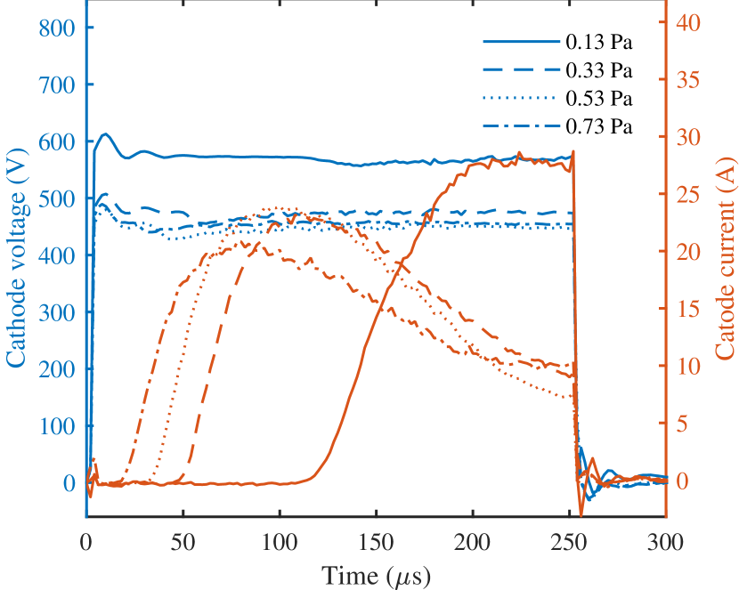
The current waveforms can be described by three distinct regions, as previously described by Lundin et al. Lundin et al. (2009) (I) plasma initiation and a current maximum, followed by (II) a decay to a minimum and then (III) a steady state regime that remains as long as the discharge voltage level is maintained. The initial peak current is a result of strong gas compression due to the rapid large flux of sputtered atoms coming from the target. Within a few s collisions of the sputtered atoms with the working gas atoms leads to heating and expansion of the working gas, known as rarefaction. As a result, the working gas atoms are replaced by the sputtered atoms in the vicinity of the cathode target to some extent as the pulse evolves. However, it has been shown that the rarefaction is primarily due to ionization losses in the target vicinity Huo et al. (2012). The rarefaction causes the discharge current to fall as can be seen for pressures in the range 0.33 – 0.73 Pa. In this regard, the 0.13 Pa case is different than for higher pressures in all three stages. This is due to a long delay on the current initiation which results in appearance of only the first stage of the discharge current during the voltage pulse. At higher pressures, the second stage is also observable, while the pulse length is not long enough to see the third stage of the current evolution. Figure 2 shows variation of the delay time and time between current initiation to peak current and 15 A as a function of Ar pressure. The current initiation delay time changes linearly in the 0.33 – 0.73 Pa range and increases dramatically at lower pressures. Previously we have reported the increased delay time with decreasing Ar pressure when sputtering a tantalum target Gudmundsson et al. (2002) and for a vanadium target in Ar/N2 mixture Hajihoseini and Gudmundsson (2017). Due to its stochastic nature, the delay time can be explained statistically as described by Yushkov and Anders Yushkov and Anders (2010). In a simplified way, the probability of ionization depends on availability of precursor, mainly represented by the pressure of the working gas and ratio of applied voltage to voltage required for ionization of the gas and sputtered atoms. Thus, Yushkov and Anders Yushkov and Anders (2010) model the inverse of delay time to be proportional to the cathode voltage. They also proposed a linear variation of delay time with inverse of pressure at constant cathode voltage. However, here we preferred to maintain constant power by increasing the cathode voltage as pressure decreases. Thus there is a competition between cathode voltage increment and pressure decrement to shorten and lengthen the delay time, respectively. Since the delay became longer as the pressure decreased, it can be concluded that in the present study the pressure has a dominant effect over cathode voltage on the length of delay time.
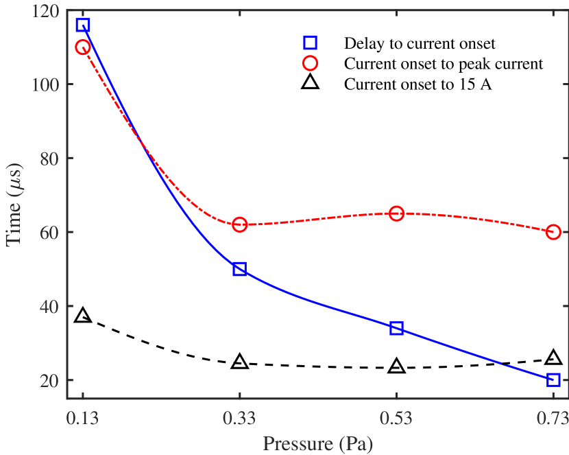
The time required to reach the peak current after current initiation is 115 s at 0.13 Pa while for higher pressures it stands nearly constant at about 75 s. Since the peak currents are not equal at different pressures, we also calculate rise time of 0 to 15 A at each pressure. The graph shows the rate of current rise is 0.41 A/s at 0.13 Pa and it increases to 0.61 A/s by increasing the pressure to 0.33 Pa. At higher pressures the current rise rate remains almost unchanged.
III.2 Microstructure
III.2.1 X-ray reflectivity
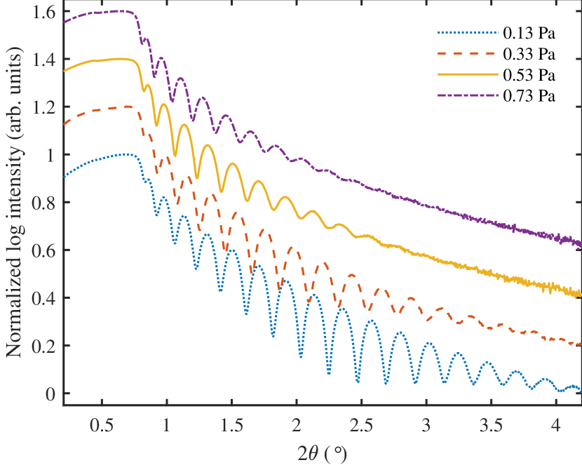
Figure 3 shows the X-ray reflectivity curves of the films grown with dcMS at room temperature as an example. The figure clearly shows a change in X-ray reflectivity with pressure. At higher pressures, the amplitude of the oscillations decays faster with incident angle, which represents greater surface roughness of the film Li et al. (2015). This behavior is reproduced similarly for the rest of the pressure series grown at different conditions but are not shown here. In order to obtain the most precise estimates of thickness, density and surface roughness of the films, the reflectivity curves have to be fitted carefully. To this end we take into account formation of an oxide layer and adsorbed moisture on its surface which is reasonable since the measurements were performed in ambient atmosphere (ex-situ).
The results of the fitting are shown in figure 4 for both of the deposition methods and both substrate temperatures. All the films were grown to the same thickness of 37 nm and the deposition rate is shown in the figure inset. We note that HiPIMS deposition has significantly lower deposition rate than dcMS deposition. As shown in figure 4(a), the density of the films grown by dcMS at room temperature shows an abrupt drop in the pressure range between 0.33 – 0.53 Pa. In contrast, utilizing HiPIMS at room temperature can maintain high density for most of the cases explored. The only exception occurs at 0.73 Pa which density shows deviation from the almost constant high density attained in other HiPIMS deposited samples. One may think that since the average deposition rate of HiPIMS is significantly lower than for dcMS (cf. figure 4(b) inset) it may result in higher densities. Thus another series was grown by dcMS at 50 W power which gives deposition rate of 0.5 Å/s equal to the average deposition rate of HiPIMS at 0.13 Pa. This lower deposition rate at 50 W dcMS improves the density at 0.13 Pa, compared to the 150 W counterpart, but the film density drops as the pressure is increased. Thus the low deposition rate is not solely responsible for the high film density obtained by HiPIMS at room temperature. For both dcMS and HiPIMS growth, increased substrate temperature seems to efficiently maintain the film density at a value very close to the bulk density of 8.72 g/cm3 (O’Handley, 2000, p. 548). 0.33 Pa which shows slight deviation from maximum density. This can be explained by the fact that at higher pressures the mean free path is reduced and an adatom experiences more collisions and loses more kinetic energy before arriving at the surface. However, raising the substrate temperature to increase the adatom mobility at the surface maintains high density of the film during growth at higher pressures.
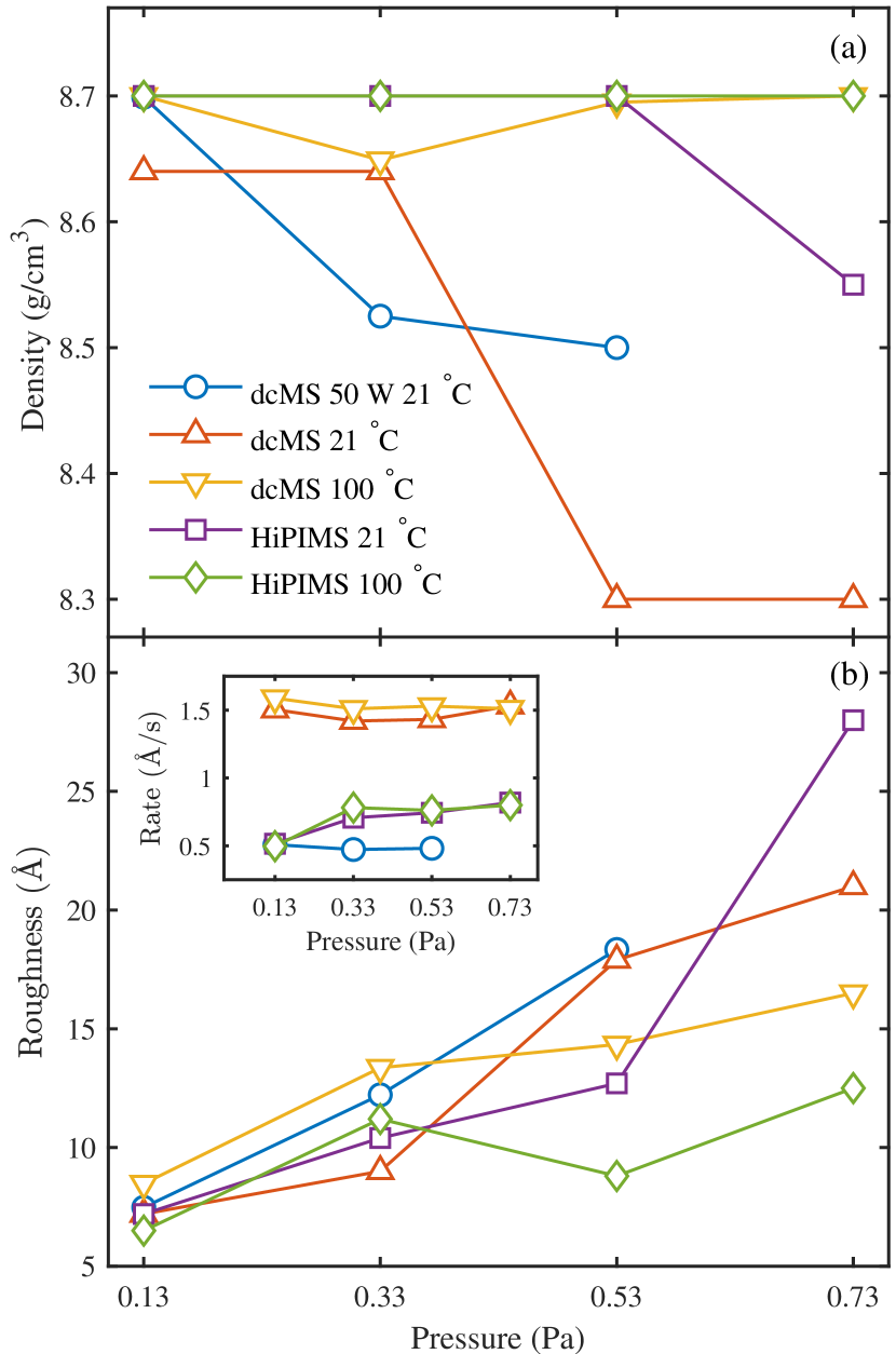
The surface roughnesses of the films grown at different conditions are shown in figure 4(b). It is worth noting that the different growth conditions have the minimum effect at the lowest pressure, 0.13 Pa, while the values are more scattered at higher pressures. In general, the trend in surface roughness is an increase with increasing pressure. Our results show precisely such a trend. Also it should be noted that films grown at C with both deposition methods show less roughness than their lower temperature counterparts grown at higher pressures. Again, this is in agreement with the statement that the more opportunity an adatom has to seek a desirable site on the surface the smoother and denser the resulting film.
For the dcMS grown films, the deposition rate is nearly independent of the pressure variation but with slightly higher values at 100 ∘C. However, the HiPIMS growth at 0.13 Pa presents considerably lower average deposition rate at both room temperature and 100 ∘C. This is due to longer delay time at 0.13 Pa which is evident from the trends shown in figures 1 and 2. We would like to remark that the average deposition rate of HiPIMS can be somewhat misleading i.e. by accounting for 100 Hz pulses of 250 s length and neglecting the delay time, the effective deposition time is below 25 ms per second which gives an effective value of 40 times the average deposition rate.
We would like to remark that utilizing a weaker magnet in the magnetron might change the behavior of the deposition rate in both dcMS and HiPIMS. For instance, we have noticed that reducing the magnet’s field strength to half the value and doubling the target thickness would result in less confinement of plasma with a linear reduction of deposition rate with pressure increment (not shown here). The linear decrease in deposition rate with increased pressure in the 1.33 – 8 Pa range was reported using HiPIMS Velicu et al. (2013). But the main focus of the current study is on the effect of pressure and substrate temperature thus we preferred a constant deposition rate to reduce the number of contributing parameters. The above mentioned effect of the magnetic field strength on HiPIMS deposition was demonstrated earlier and the interested reader is referred to our earlier work on VN deposition Hajihoseini and Gudmundsson (2017) for further information.
III.2.2 X-ray diffraction
Figure 5 shows two sets of GIXRD patterns, namely different films grown at fixed pressure of 0.13 Pa with dcMS and HiPIMS at varying temperature and for films grown by HiPIMS at 100∘C at different pressures. Results for other films are not shown here since they show very little difference. The figure insets depict the variation in the (111) peak intensity and estimated grain size from the Scherrer equation (Langford and Wilson, 1978), which has been proven to give quantitatively correct values for Py films (Neerinck et al., 1996), with pressure for all of the films. The three main peaks are evident in all cases those are located at 44.217, 51.518 and 75.845∘ corresponding to (111), (200) and (220) planes, respectively Dzhumaliev et al. (2016). The dominant peak is (111) in all cases. The (111) texture provides perpendicular anisotropy to the Py films as for fcc alloy structures the direction is the easy magnetization axis (O’Handley, 2000, p. 224). This becomes important for films somewhat thicker than ours and plays an important role in stripe domain formation. It has been shown for films grown by normal deposition geometry, that an increase in the pressure reduces the peak height and this is most pronounced for the (111) peak Svalov et al. (2010). Only our dcMS grown films at room temperature are in agreement with those results. In contrast, maximum (111) peak intensity is obtained at 0.33 Pa for dcMS grown films at 100 ∘C, and at 0.73 Pa for the films grown by HiPIMS at both room temperature and 100 ∘C. The (200) peak intensity shows a slight increase while (220) peak intensity presents a decrease with increasing pressure for all the films (not shown here).
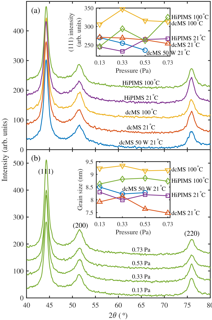
A more quantitative understanding of the film crystallinity is represented by the grain size. The estimated grain size from the (111) peaks shows negligible variation with pressure. It is also worth noting that dcMS growth results in smaller grain size at room temperature than HiPIMS while it gives larger grain size at 100 ∘C. Thus increasing the substrate temperature has a more pronounced effect in the grain growth during dcMS deposition.
III.3 Magnetic properties
III.3.1 Anisotropy and coercive fields
Figure 6 shows the variation of the anisotropy field and coercivity with pressure for both dcMS and HiPIMS grown films. The results are extracted from hysteresis loops measured along easy and hard axis of the film using MOKE. It can be clearly seen that increases with increased pressure for films grown by dcMS at room temperature. All our other films have either a nearly constant (dcMS and HiPIMS at 100 ∘C) or a delayed and slower growth as function of pressure as in the case of the HiPIMS grown film at room temperature. Both increased substrate temperature and the higher ion energy involved in HiPIMS deposition contribute to more adatom surface diffusion, encouraging defect-free crystal growth that helps to maintain the low anisotropy field .
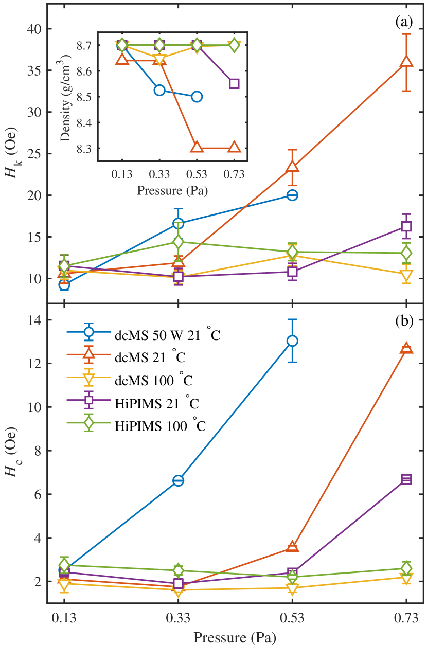
It has been shown previously, that associated with void formation there is an increase in the anisotropy field in Py Sugita et al. (1967); Fujiwara and Sugita (1968). Our quantitative results are in good agreement with their interpretation. The density results shown in the inset in figure 6 (a) show that the density remains high for the films that exhibit low but drops in the cases where there is an increase in . Presumably the lower density is associated with more defective crystal growth and void formation. Considering the fact that surface roughness increases with pressure in all cases (cf. figure 4(b)), our results are inconsistent with the results of Choe and Steinback Choe and Steinback (1999) who found a linear reduction in with increased surface roughness. A reason for this difference might be the film thickness i.e. their films were 15 nm thick which makes them more sensitive to the surface properties compared to 37 nm films here which are more influenced by “bulk-like” properties. Thus, knowing that the grain size is nearly constant for each pressure series (as shown in figure 5 inset) the variation of here is associated with the density of the films. The high film density is maintained in 0.13 Pa films using HiPIMS and also dcMS at 100 ∘C while the is low.
The variation of with pressure is shown in figure 6(b). It is clear that at a certain threshold pressure there is a density reduction accompanied by an increase in for films grown at room temperature. For the dcMS films this threshold pressure is at 0.13 and 0.53 Pa, respectively for 50 and 150 W power, while for the room temperature HiPIMS sample it is at 0.73 Pa. Again due to higher film density for growth at 100 ∘C, the low is maintained at high pressures. Based on surface roughness Choe and Steinback Choe and Steinback (1999) reported two regions: (I) below 8 Å surface roughness where slightly increases with surface roughness and (II) surface roughnesses higher than 8 Å where increases dramatically with surface roughness, due to surface roughness induced pinning of domain walls during magnetization reversal. This is not the case in our results. For instance HiPIMS grown film at 21 ∘C and 0.73 Pa present highest roughness of the all films while it presents an intermediate compared to the dcMS counterpart. In the present results, the pinning is attributed to voids and defects appearing in films with low mass density.
III.3.2 Magnetization traces
In addition to desirable values of and , for many applications it is also important to have well defined magnetic axes. Figure 7 shows the average of a few loops obtained by MOKE measurements for room temperature grown films. Similar results were obtained for films grown at 100 ∘C, that are not shown here. The dotted lines belong to dcMS grown films which always present higher saturation fields than their HiPIMS counterparts grown at the same pressure, shown by dashed lines. This is more evident at higher pressures of 0.53 and 0.73 Pa shown in yellow and purple, respectively.
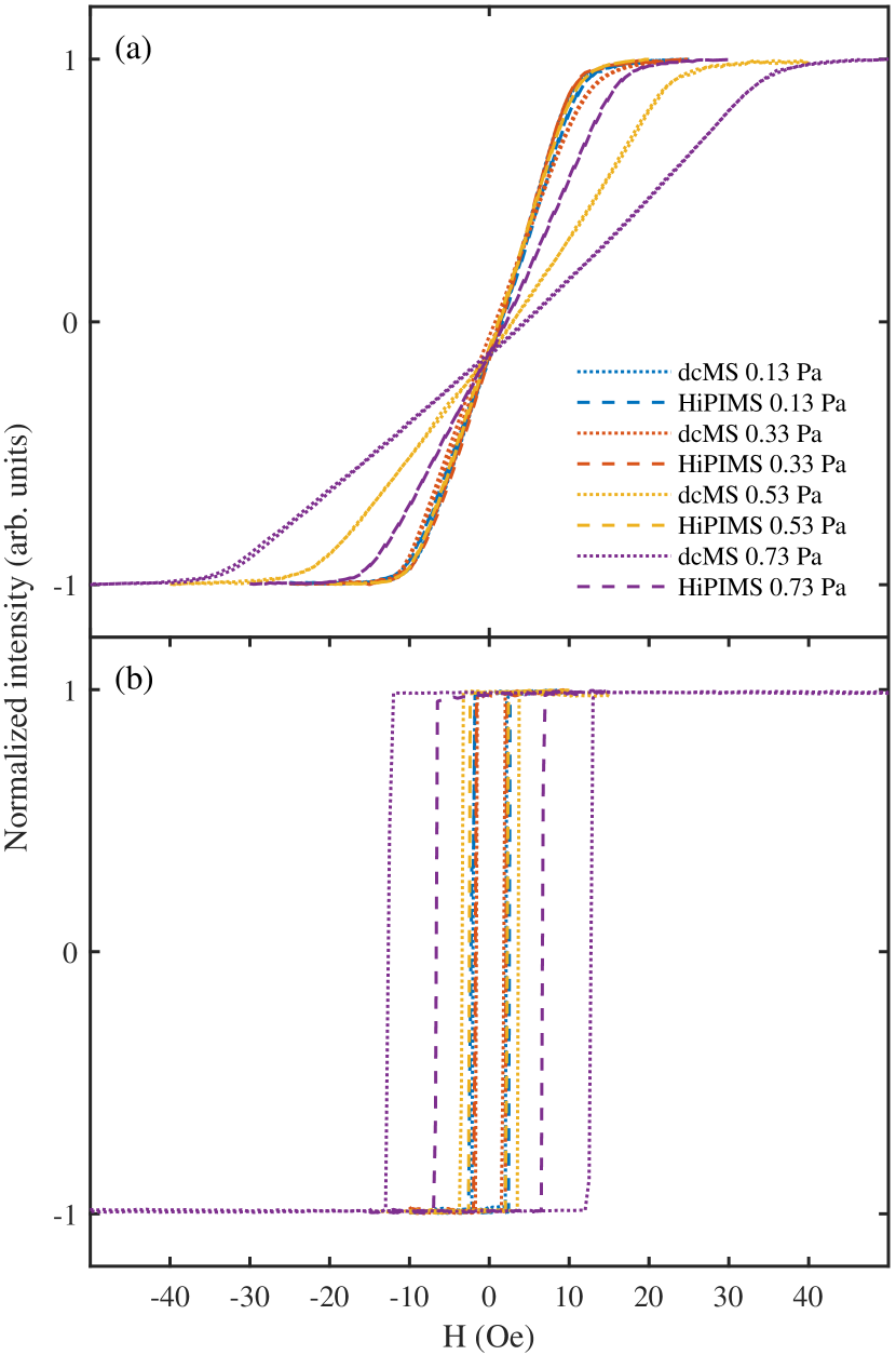
It can be seen that in both methods, deposition under an angle provides a linear non-hysteretic hard axis and a square easy axis with sharp transitions. However, it has been shown previously that dcMS deposition normal to substrate at high pressure with in-situ magnetic field, gives open hard axis and rounded easy axis traces Svalov et al. (2010). We have shown previously that at low pressures (0.13 Pa) the effect of deposition under an angle on the direction of the magnetization axis can be stronger than the effect of an in-situ magnetic field during growth Kateb and Ingvarsson (2017); Kateb et al. (2018). The present results show that uniaxial anisotropy induced by tilt deposition maintains the shape of loops at different pressures. Although we have detected an increase in both and in some of the samples grown at room temperature (cf. figure 6) there is no indication of out-of-plane magnetization or poorly defined uniaxial anisotropy in those samples.
IV Conclusions
We have demonstrated the deposition of Ni80Fe20 thin films using high power impulse magnetron sputtering, HiPIMS. For comparison we also deposited films using dc magnetron sputtering under the same conditions, i.e. to the same thickness, at the same pressure, substrate temperature, tilt angle and with power identical to the HiPIMS average power. We compared the results of structural characterization (X-ray) and magnetic properties. The results indicate that the higher the adatom energy, as it meets with the sample substrate/film, the denser the film, accompanied with low coercive and anisotropy fields. All conditions kept the same, the HiPIMS deposition method gives a higher adatom energy than dcMS. Increased adatom energy can also be achieved by raising the deposition temperature or lowering the pressure. In accordance with this our results show a drop in film density for samples deposited at room temperature (our lowest deposition temperature) with increasing pressure, accompanied by a rise in both coercive and anisotropy fields.
Acknowledgements.
This work was partially supported by the University of Iceland Research Funds for Doctoral students, the Icelandic Research Fund Grants Nos. 130029 and 120002023, and the Swedish Government Agency for Innovation Systems (VINNOVA) contract no. 2014-04876.References
- McGuire and Potter (1975) T. McGuire and R. Potter, IEEE Transactions on Magnetics 11, 1018 (1975).
- Andricacos and Robertson (1998) P. C. Andricacos and N. Robertson, IBM Journal of Research and Development 42, 671 (1998).
- Craus et al. (2005) C. B. Craus, T. Onoue, K. Ramstöck, W. G. M. A. Geerts, M. H. Siekman, L. Abelmann, and J. C. Lodder, Journal of Physics D: Applied Physics 38, 363 (2005).
- Cooper et al. (2005) E. I. Cooper, C. Bonhote, J. Heidmann, Y. Hsu, P. Kern, J. W. Lam, M. Ramasubramanian, N. Robertson, L. T. Romankiw, and H. Xu, IBM Journal of Research and Development 49, 103 (2005).
- Yokoshima (2010) T. Yokoshima, in Electrochemical Nanotechnologies, edited by T. Osaka, M. Datta, and Y. Shacham-Diamand (Springer-Verlag, New York, 2010), pp. 67 – 85.
- Åkerman (2005) J. Åkerman, Science 308, 508 (2005).
- Wang et al. (2017) J. Wang, X. Zhang, X. Lu, J. Zhang, Y. Yan, H. Ling, J. Wu, Y. Zhou, and Y. Xu, Applied Physics Letters 111, 072401 (2017).
- Umezaki et al. (1982) H. Umezaki, H. Nishida, N. Tsumita, N. Koyama, H. Nozawa, and Y. Sugita, IEEE Transactions on Magnetics 18, 753 (1982).
- Sugita et al. (1967) Y. Sugita, H. Fujiwara, and T. Sato, Applied Physics Letters 10, 229 (1967).
- Shimokawa et al. (2012) T. Shimokawa, T. Yanai, K. Takahashi, M. Nakano, K. Suzuki, and H. Fukunaga, IEEE Transactions on Magnetics 48, 2907 (2012).
- Theis et al. (2013) M. Theis, S. Ediger, M. T. Schmitt, J.-E. Hoffmann, and M. Saumer, physica status solidi (a) 210, 853 (2013).
- Yanai et al. (2018) T. Yanai, K. Eguchi, K. Koda, J. Kaji, H. Aramaki, K. Takashima, M. Nakano, and H. Fukunaga, AIP Advances 8, 056123 (2018).
- Watanabe et al. (2005) G. Watanabe, S. Koizumi, T. Yamada, Y. Takemura, and J. Shirakashi, Journal of Vacuum Science and Technology B 23, 2390 (2005).
- Collins et al. (1981) A. J. Collins, C. J. Prior, and R. C. J. Hicks, Thin Solid Films 86, 165 (1981).
- Yang and Aboaf (1989) M. M. Yang and J. A. Aboaf, Journal of Applied Physics 66, 3734 (1989).
- Pötzlberger (1984) H. W. Pötzlberger, IEEE Transaction on Magnetics 20, 851 (1984).
- Rijks et al. (1997) T. G. S. M. Rijks, S. K. J. Lenczowski, R. Coehoorn, and W. J. M. de Jonge, Physical Review B 56, 362 (1997).
- Svalov et al. (2010) A. Svalov, I. Aseguinolaza, A. Garcia-Arribas, I. Orue, J. Barandiaran, J. Alonso, M. Fernández-Gubieda, and G. Kurlyandskaya, IEEE Transactions on Magnetics 46, 333 (2010).
- Chaug and Williamson (1990) Y.-S. Chaug and D. L. Williamson, Journal of Vacuum Science and Technology A 9, 505 (1990).
- Kateb and Ingvarsson (2017) M. Kateb and S. Ingvarsson, in 2017 IEEE Sensors Applications Symposium (SAS) (IEEE, Glassboro, New Jersey, 2017), pp. 1–5.
- Kateb et al. (2018) M. Kateb, E. Jacobsen, and S. Ingvarsson, Journal of Physics D: Applied Physics 52, 075002 (2018).
- Barranco et al. (2016) A. Barranco, A. Borras, A. R. Gonzalez-Elipe, and A. Palmero, Progress in Materials Science 76, 59 (2016).
- Fujiwara and Sugita (1968) H. Fujiwara and Y. Sugita, IEEE Transactions on Magnetics 4, 22 (1968).
- Kools (1995) J. Kools, Journal of Applied Physics 77, 2993 (1995).
- Helmersson et al. (2006) U. Helmersson, M. Lattemann, J. Bohlmark, A. P. Ehiasarian, and J. T. Gudmundsson, Thin Solid Films 513, 1 (2006).
- Gudmundsson et al. (2012) J. T. Gudmundsson, N. Brenning, D. Lundin, and U. Helmersson, Journal of Vacuum Science and Technology A 30, 030801 (2012).
- Samuelsson et al. (2010) M. Samuelsson, D. Lundin, J. Jensen, M. A. Raadu, J. T. Gudmundsson, and U. Helmersson, Surface and Coatings Technology 205, 591 (2010).
- Magnus et al. (2011) F. Magnus, A. S. Ingason, O. B. Sveinsson, S. Olafsson, and J. T. Gudmundsson, Thin Solid Films 520, 1621 (2011).
- Magnus et al. (2012) F. Magnus, A. S. Ingason, S. Olafsson, and J. T. Gudmundsson, IEEE Electron Device Letters 33, 1045 (2012).
- Alami et al. (2005) J. Alami, P. O. Å. Persson, D. Music, J. T. Gudmundsson, J. Bohlmark, and U. Helmersson, Journal of Vacuum Science and Technology A 23, 278 (2005).
- Hajihoseini and Gudmundsson (2017) H. Hajihoseini and J. T. Gudmundsson, Journal of Physics D: Applied Physics 50, 505302 (2017).
- Velicu et al. (2012) I.-L. Velicu, M. Neagu, H. Chiriac, V. Tiron, and M. Dobromir, IEEE Transactions on Magnetics 48, 1336 (2012).
- O’Handley (2000) R. C. O’Handley, Modern Magnetic Materials: Principles and Applications (John Wiley & Sons, 2000).
- Velicu et al. (2013) I.-L. Velicu, M. Kowalczyk, M. Neagu, V. Tirona, H. Chiriac, and J. Ferenc, Materials Science and Engineering B 178, 1329 (2013).
- Parratt (1954) L. G. Parratt, Physical Review 95, 359 (1954).
- Lundin et al. (2009) D. Lundin, N. Brenning, D. Jadernas, P. Larsson, E. Wallin, M. Lattemann, M. A. Raadu, and U. Helmersson, Plasma Sources Science and Technology 18, 045008 (2009).
- Huo et al. (2012) C. Huo, M. A. Raadu, D. Lundin, J. T. Gudmundsson, A. Anders, and N. Brenning, Plasma Sources Science and Technology 21, 045004 (2012).
- Gudmundsson et al. (2002) J. T. Gudmundsson, J. Alami, and U. Helmersson, Surface and Coatings Technology 161, 249 (2002).
- Yushkov and Anders (2010) G. Y. Yushkov and A. Anders, IEEE Transactions on Plasma Science 38, 3028 (2010).
- Li et al. (2015) W. Li, X. Yan, A. G. Aberle, and S. Venkataraj, Japanese Journal of Applied Physics 54, 08KC14 (2015).
- Langford and Wilson (1978) J. I. Langford and A. Wilson, Journal of Applied Crystallography 11, 102 (1978).
- Neerinck et al. (1996) D. G. Neerinck, A. E. M. De Veirman, M. H. J. Slangen, T. G. S. M. Rijks, and J. C. S. Kools, Thin Solid Films 280, 136 (1996).
- Dzhumaliev et al. (2016) A. Dzhumaliev, Y. V. Nikulin, and Y. A. Filimonov, Physics of the Solid State 58, 1053 (2016).
- Choe and Steinback (1999) G. Choe and M. Steinback, Journal of Applied Physics 85, 5777 (1999).