Nonradiative emission and absorption rates of quantum emitters embedded in metallic systems: microscopic description and their determination from electronic transport
Abstract
We investigate nonradiative emission and absorption rates of two-level quantum emitters embedded in a metal at low temperatures. We obtain the expressions for both nonradiative transition rates and identify a unique, experimentally accessible way to obtain the nonradiative decay rates via electronic transport in the host metallic system. Our findings not only provide a microscopic description of nonradiative decay channels in metals, but they also allows one to identify and differentiate them from other decay channels, which is crucial to understand and control light-matter interactions at the nanoscale.
I Introduction
Controlling and understanding light-matter interactions at the nanoscale is key for a broad range of applications, including biosensing, imaging, and quantum information processing. Among the several processes that govern light-matter interactions, spontaneous emission from Quantum Emitters (QE) (atoms, molecules, and quantum dots) is one of the most important for applications in nanophotonics. This radiative process strongly depends on the electromagnetic environment of the QE, as discovered in the pioneering work by Purcell Purcell-46 , and it has been extensively investigated in several photonic systems, such as photonic cavities bjork1991 ; gerard1998 , planar interfaces urbach1998 ; johansen2008 , photonic crystals yablonovitch1987 ; lodahl2004 , metamaterials klimov2002 ; hyperbolicreview ; jacob2012 ; kortkamp2013 , and waveguides chen2010 ; kumar2013 .
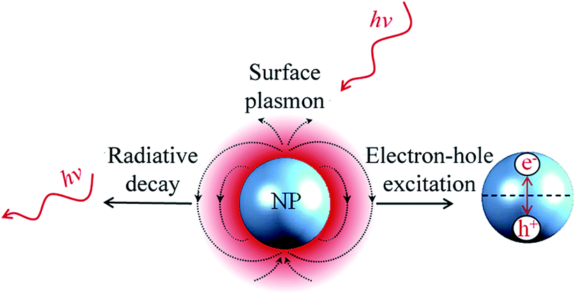
In addition to the radiative relaxation, when the QE is placed near or inside metallic structures other decay pathways are available, see Fig. (1). In this case the energy of the QE can be dissipated in a plasmonic channel. For instance, the proximity of a QE to metal-dielectric interfaces facilitates the excitation of surface plasmon polaritons, electromagnetic excitations related to the charge density waves on the surface of the metallic structure. This mechanism leads to a strong confinement of the electromagnetic field at metal-dielectric interfaces, which is the basis of many applications to enhance light-matter interactions, such as single optical plasmon generation akimov2007 ; chang2006 , single molecule detection with surface-enhanced Raman scattering nie1997 , and nanoantenna modified spontaneous emission taminiau2008 .
Nonradiative relaxation is another decay pathway, where the QE energy can be dissipated via coupling to phonons, resistive heating, or quenching by other quantum emitters. Nonradiative relaxation is particularly important in metallic systems, where emission quenching may occur due to unavoidable dissipation even in systems with high spontaneous emission rate. In many cases of practical interest increasing the ratio between radiative and nonradiative decay channels is of great importance since the former actually determines the efficiencies of photonic devices, such as LEDs fan1997 , and single-photon sources eisaman2011 . In other situations it is very important to identify the nonradiative mechanism, distinguishing it from the plasmonic channel as it is the case of applications involving the excitation of single plasmon polaritons and subsequent controlled coupling between metallic nanowires kumar2014 ; pors2015 .
In the present paper we identify a unique, experimentally accessible way to identity the nonradiative contribution to the total decay of QE inside metals. The situation in which the QE is embedded in metallic systems is within the reach of current nanofabrication techniques and is of increasing importance in applications involving metamaterials roth2017 . By means of a microscopic, analytical approach, we compute the nonradiative decay channel of a QE embedded in a metal, in which dissipation is due to inelastic scattering of electrons close to the Fermi surface, see Fig. (1) figure1 . After computing the transition rates for both nonradiative emission and absorption, we demonstrate that such quantities can be directly determined by the knowledge of experimentally accessible transport quantities, such as the optical and ac-conductivity, and even the dc-resistivity. This result not only provides a microscopic description of nonradiative decay channels in metals, but also allows one to identify and differentiate it to other decay channels, which is crucial for the development of disruptive optoelectronic plasmonic applications.
This paper is organized as follows. In Sec. II we describe the methodology to microscopically calculate the transition rates for both nonradiative emission and absorption. In Sec. III we discuss and analyze the behavior of the decay rates as a function of the temperature, whereas Sec. IV is devoted to the conclusions.
II Methodology
We consider a two-level QE embedded in a metal in which relaxation can occur via the inelastic scattering of electrons close to the Fermi surface, as it is schematically illustrated at the right side of Fig. (1). To model the coupling between the QD with the band electrons in a metal, let us considering the following interaction Hamiltonian:
| (1) |
where is the energy splitting of the two level system, is the band dispersion relation for the electrons in the metal, and are creation and anihilation operators such that
| (2) |
with representing the Fermi sea, representing the hole state, representing the particle state, and with being the Fermi-Dirac occupation probability. For simplicity, we shall omit spin indices since we will be considering solely spin preserving scattering processes. The interaction part of the Hamiltonian reads
| (3) |
and describes the electrostatic interaction between an electronic charge density for electrons in a metal and the potential generated by the two level system. Here and are the projection operators onto the ground, , and excited, , states, while and describe the electronic tunneling between the two levels. We have also introduced the impurity structure factor
| (4) |
where gives the probability of having an emitter at .
In what follows we shall be interested in calculating the nonradiative emission and absorption rates and, for this reason, we will restrict our calculations to the and processes only, both associated to the matrix element (within the dipole approximation of the electrostatic Coulomb potential)
| (5) |
describing the electron-atom coupling, where is the electric charge, is the volume, is the vacuum dielectric constant, is the relative permissivity in the medium, is the electric dipole moment of the emitter and
| (6) |
is the unit vector along the direction of . For future purposes it will be interesting to observe that the interacting part of the Hamiltonian has the general structure
| (7) |
and that the eigenstates of the free Hamiltonian are written as
| (8) |
where with are the eigenvectors of the TLS Hamiltonian, and are the eigenvectors of the electron Hamiltonian in the number operator representation.
III Results and discussions
III.1 General structure for the non radiative decay rate
For the above interaction Hamiltonian, with initial and final states corresponding to
| (9) |
where, , and with energies
the transition amplitude can be calculated from Fermi’s golden rule
The matrix element can be calculated with the use of the fermionic algebra (2) and from the fact that , for a small number of dilute impurities (emitters). We are now ready to rewrite the transition amplitude in terms of the initial and final momentum states, representing the hole state, representing the electron state, and in terms of the occupation probabilities for the ground, , and excited, , states in the two-level system
| (10) | |||||
The next step is to calculate the relaxation rates through summing up transition amplitudes using the relation
| (11) |
where the factor accounts for spin degeneracy, is the velocity for a nearly free electron, parabolic band approximation with effective mass , and
| (12) |
For the nonradiative (nr) decay from the excited to ground states we thus have
We identify the electronic density of states at the Fermi level
| (13) |
and we have defined the quantity
| (14) |
in terms of the Thomas-Fermi screening length . Now the nonradiative decay rate is simply
| (15) |
To arrive at the above result we have used that, at low temperatures, the function
| (16) |
is strongly peaked around the Fermi energy and thus we projected all states and . Furthermore, we calculated
| (17) |
III.2 General structure for the non radiative absorption rate
Similarly to the result obtained above, the nonradiative absorption rate is given by
| (18) |
where and have been interchanged and the thermal factor is also different
| (19) |
satisfying detailed balance.
III.3 Normalized decay and absorption rates
A meaningful quantity to be defined is the nonradiative decay rate normalized by its saturation value
| (20) |
since, for , and . With this definition we arrive at
| (21) |
which is a dimensionless number between and . The same is valid for the absorption rate
| (22) |
The results for both nonradiative emission and absorption rates, as well as their sum, are plotted in the inset of Fig. 2. We can also study the difference between the nonradiative absorption and emission rates
| (23) |
which is a quantity between and and is plotted as the main panel in Fig. 2.
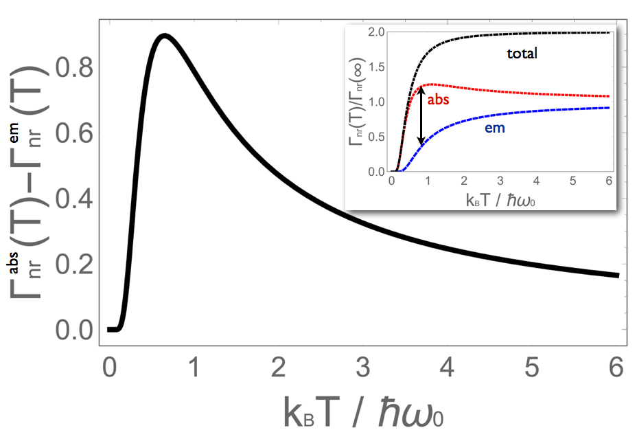
Figure 2 reveals that the absorption processes, in which a recombination of a particle and a hole provides energy for the transition, dominates for . Absorption rapidly increases with temperature, but eventually saturates due to the decrease in the thermal occupation of the ground state for . On the other hand, emission processes in which a particle and a hole are created, receiving energy from the transition, are less frequent at all temperatures because of the lower thermal occupation in the excited state of the emitter. Nevertheless, it also increases with the temperature and also saturates for . Remarkably, let us point out that such large difference between the absorption and emission rates indicates that the phenomenon of generation is occurring at the emitter due to the inelastic scattering from Fermi surface states at low temperatures. This result suggests one can prepare the emitter in excited state by setting the temperature around , which may find potential applications in quantum nanophotonics.
IV Connection to electronic transport
Let us now see how we can extract information about the non radiative transition rates from dc- and magneto-transport experiments. We shall first look into the dc-transport, with an externally applied electric field, , where the resistivity
| (24) |
is given in terms of the inverse transport lifetime, , with being the effective mass, the electronic density and the electric charge. The quantity of interest will be the inverse transport lifetime, , which can be calculated using a variational approach to the linearized Boltzmann’s transport equations within the relaxation time approximation allen . Next, we shall focus on the magneto-transport, with externally applied electric, , and magnetic, , fields, where the Shubnikov-de-Haas oscillations sdho ; deltaRxx
| (25) |
are given in terms of the quantum lifetime, , with being the zero field resistance, the ciclotron frequency, and , a the thermal damping factor. The quantity of interest here is the inverse quantum lifetime, , which can also be calculated using a variational procedure allen . For both cases (dc- and magneto- transport) we shall explain how the non radiative transition rates calculated earlier can be extracted from experiments.
IV.1 Connection to transport lifetime
According to the interaction Hamiltonian (3) there are four channels for scattering between the emitter and Fermi surface electrons: two elastic channels, and , and two inelastic channels, (absorption) and (emission). The inverse transport lifetime, , can thus be calculated using Mathiessen’s rule
| (26) |
in which each individual contribution, , to the total inverse scattering time can be calculated from a variational principle to the linearized Boltzmann’s equations within the relaxation time approximation allen
| (27) |
where corresponds to the direction of the applied electric field, and are the scattering amplitudes from to , between states labelled by .
The denominator in (27) can be written as
| (28) |
where is the electronic density of the Fermi system, and the factor arises from the spherical symemtry of the problem. As for the numerator in (27) we shall write
| (29) |
where the scattering amplitudes are
| (30) |
| (31) |
| (32) |
| (33) |
In this case, for the two elastic scattering processes we find
| (34) | |||||
and
| (35) | |||||
where
| (36) |
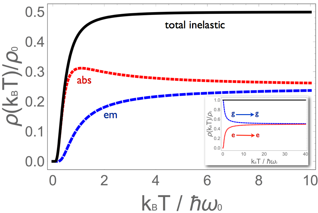
The elastic contributions to the resistivity are shown in the inset of Fig. 3. As we can see, the sum of the two elastic contributions is temperature independent mostly because and , even though each of the two individual scattering channels exhibits a characteristic evolution with the temperature until saturation at for . Furthermore, since this contribution has its origins in elastic processes, and do not contain information about the structure of the emitter, neither through the electric dipole moment, , nor through the characteristic energy of the emitter, . Hence the elastic contributions to the resistivity have no connection to the transition rates calculated earlier.
For the two inelastic scattering processes we have
| (37) | |||||
and
| (38) | |||||
where
| (39) | |||||
The inelastic contributions to the resistivity are shown in the main panel of Fig. 3. In contrast to the elastic case, both the individual contributions to the resistivity, as well as their sum, have a strong temperature dependence that is analogous to the temperature dependence of the normalized emission and absorption rates shown in Fig. 2.
Also differently to the elastic case, the inelastic contributions and do carry information about the structure of the emitter, through both the electric dipole moment, , and the characteristic energy, . Indeed, it is important to note the direct connection that exists between the non-radiative decay rate, given by (14) and (15), and the inelastic scattering process given by (38). Both quantities are proportional to and only differ by a constant factor that is fixed by the Fermi wave vector, , and the Thomas-Fermi screening length, , see in (14) and in (39). By the same token, a similar mapping exists between the nonradiative absorption rate (18) and the other inelastic scattering process, given by (37). Again, these two quantities only differ by a constant factor. Altogether these findings unveil the relation between nonradiative decay and absorption rates and the inelastic scattering processes, suggesting that one can obtain information about nonradiative decay by means of electronic transport.
IV.2 Connection to quantum lifetime
Similar to the case of the dc-resistivity, the quantum lifetime can also be calculated, using Mathiessen’s rule
| (40) |
where now each contribution corresponds to allen
| (41) |
Again, for the numerator in (41) we define
| (42) |
For the two inelastic scattering processes we obtain
| (43) | |||||
and
| (44) | |||||
where
| (45) |
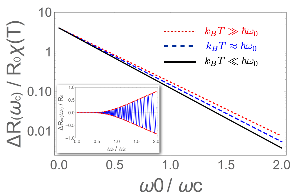
Remarkably, we now obtain that for the quantum lifetime, , there exists a one-to-one correspondence between the nonradiative emission and absorption rates, and , and the inelastic contributions to electron-impurity scattering processes, and . These results confirm our predictions that one can determine the nonradiative emission and absorption rates by means of magneto-transport observables such as, for example, the amplitude of the Shubnikov-de-Haas oscillations which is given by dingle
| (46) |
which is governed by and it is shown in the main panel of Fig. (4). From such a Dingle plot dingle , we see that, already at small magnetic fields, , even the smallest contributions to the quantum lifetime, , from nonradiative transitions may lead to sizeble deviations of the amplitude of the Shubnikov-de-Haas oscillations from the pure elastic case at . If we recall that, for absorption processes dominate, as demonstrated in Fig. (2), we can promptly identify that the deviation of the dashed (blue) curve from the solid (black) curve in Fig. (4) is predominantly due to absorption processes, . On the other hand, for the dotted (red) curve in Fig. (4), valid for , both emission and absorption processes contribute equally, so that . These findings suggest one can not only extract nonradiative decay rates from the Shubnikov-de-Haas oscillations via the quantum lifetime, but also detect the presence of the emitters inside a metallic system, as nonradiative decay rates strongly depend on temperature, as we previously demonstrate.
V Conclusions
In summary, we investigate nonradiative emission and absorption rates of two-level quantum emitters embedded in a metal at low temperatures. Using Fermi’s golden rule, we derive expressions for both nonradiative transition rates, showing they are intrinsically related to electronic transport in the host metallic material. Indeed, we demonstrate nonradiative emission and absorption rates could be directly determined by the knowledge of experimentally accessible transport quantities, such as the optical and ac-conductivity, and even the dc-resistivity. For concreteness, we consider the case of Shubnikov-de-Haas oscillations, governed by the quantum lifetime, which we demonstrate to be proportional to the nonradiative emission and absorption rates. Altogether our results not only provide a microscopic description of nonradiative decay channels in metals, but they also allows one to identify and differentiate them to other decay channels, which is crucial to understand and control light-matter interactions at the nanoscale.
Acknowledgements.
We thank F.S.S. Rosa, C. Farina, and L.S. Menezes for fruitful discussions. We acknowledge CNPq, CAPES, and FAPERJ for financial support. F.A.P. also thanks the The Royal Society-Newton Advanced Fellowship (Grant no. NA150208) for financial support.References
- (1) E. M. Purcell, Phys. Rev. 69, 681 (1946).
- (2) G. Bjork, S. Machida, Y. Yamamoto, and K. Igeta, Phys. Rev. A 44, 669 (1991).
- (3) J. M. Gérard, B. Sermage, B. Gayral, B. Legrand, E. Costard, and V. Thierry-Mieg, Phys. Rev. Lett. 81, 1110 (1998).
- (4) H. P. Urbach and G. L. J. A. R. Rikken, Phys. Rev. A 57, 3913 (1998).
- (5) J. Johansen, S. Stobbe, I. S. Nikolaev, T. Lund-Hansen, P. T. Kristensen, J. M. Hvam, W. L. Vos, and P. Lodahl, Phys. Rev. B 77, 073303 (2008).
- (6) E. Yablonovitch, Phys. Rev. Lett. 58, 2059 (1987).
- (7) P. Lodahl, A. F. van Driel, I. S. Nikolaev, A. Irman, K. Overgaag, D. Vanmaekelbergh, and W. L. Vos, Nature 430, 654 (2004).
- (8) V. V. Klimov, Opt. Commun. 211, 183 (2002).
- (9) C.L. Cortes, W. Newman, S. Molesky, and Z. Jacob, J. Opt. 14, 063001 (2012).
- (10) Z. Jacob, I. I. Smolyaninov, and E. E. Narimanov, Appl. Phys. Lett. 100, 181105 (2012).
- (11) W. J. M. Kort-Kamp, F. S. S. Rosa, F. A. Pinheiro, and C. Farina, Phys. Rev. A 87, 023837 (2013).
- (12) Y. Chen, T. R. Nielsen, N. Gregersen, P. Lodahl, J. Mork, Phys. Rev. B 81, 125431 (2010).
- (13) S. Kumar, A. Huck, U. L. Andersen, Nano Lett. 13, 1221 (2013).
- (14) A. V. Akimov, A. Mukherjee, C. L. Yu, D. E. Chang, A. S. Zibrov, P. R. Hemmer, H. Park, and M. D. Lukin, Nature (London) 450, 402 (2007).
- (15) D. E. Chang, A. S. Sorensen, P. R. Hemmer, and M. D. Lukin, Phys. Rev. Lett. 97, 053002 (2006).
- (16) S. Nie and S. R. Emory, Science 275, 1102 (1997).
- (17) T. H. Taminiau, F. D. Stefani, F. B. Segerink, and N. F. van Hulst, Nat. Photonics 2, 234 (2008).
- (18) S. Fan, P. R. Villeneuve, J. D. Joannopoulos, E. F. Schubert, Phys. Rev. Lett. 78, 3294 (1997).
- (19) M. D. Eisaman, J. Fan, A. Migdall, S. V. Polyakov, Rev. Sci. Instrum. 82, 071101 (2011).
- (20) S. Kumar, N. I. Kristiansen, A. Huck, U. L. Andersen, Nano Lett. 14, 663 (2014).
- (21) A. Pors and S. I. Bozhevolnyi, ACS Photonics 2, 228 (2015).
- (22) D. J. Roth, A.V. Krasavin, A. Wade, W. Dickson, A. Murphy, S. K ’ena-Cohen, R. Pollard, G. A. Wurtz, D. Richards, S. A. Maier, A. V. Zayats, ACS Photonics 4, 2513 (2017).
- (23) M. Valenti, M. P. Jonsson, G. Biskos, A. Schmidt-Ott, and W. A. Smith, J. Mater. Chem. A 4, 17891 (2016).
- (24) Phillip B. Allen, in Quantum Theory of Real Materials, chapter 17, 219-250, edited by J. R. Chellkowsky and S. G. Loule, Kluwer, Boston, 1996.
- (25) L. Shubnikov and W. de Haas, Leiden Communication 207a, 3 (1930).
- (26) A. Isihara and L. Smrcka, J. Phys. C: Solid State Phys. 19, 6777 (1986).
- (27) P. T. Coleridge, R. Stoner, and R. Fletcher, Phys. Rev. B39, 1120 (1989); P. T. Coleridge, Phys. Rev. B44, 3793 (1991).