Maximum reflectance and transmittance of films coated with gapped graphene in the context of Dirac model
Abstract
The analytic expressions for the maximum and minimum reflectance of optical films coated with gapped graphene are derived in the application region of the Dirac model with account of multiple reflections. The respective film thicknesses are also found. In so doing the film material is described by the frequency-dependent index of refraction and graphene by the polarization tensor defined along the real frequency axis. The developed formalism is illustrated by an example of the graphene-coated film made of amorphous silica. Numerical computations of the maximum and minimum reflectances and respective film thicknesses are performed at room temperature in two frequency regions belonging to the near-infrared and far-infrared domains. It is shown that in the far-infrared domain the graphene coating makes a profound effect on the values of maximum reflectance and respective film thickness leading to a relative increase of their values by up to 65% and 50%, respectively. The maximum transmittance of a graphene-coated film of appropriately chosen thickness is shown to exceed 90%. Possible applications of the obtained results are discussed.
I INTRODUCTION
The discovery of graphene has already initiated a wide range of both experimental and theoretical investigations (see, e.g., the monographs 1 ; 2 and reviews 3 ; 4 ; 5 ; 6 ). Graphene is a two-dimensional sheet of carbon atoms packed in a hexagonal lattice. The most outstanding feature of graphene is that at energies below 1–2 eV its electronic and optical properties are well described by the Dirac model. This model assumes that the quasiparticles in graphene are massless or very light and obey the linear dispersion relation. Thus, they are described not by the Schrödinger equation, as quasiparticles in all 3D-materials, but by the Dirac equation, where the speed of light is replaced with the Fermi velocity 1 ; 2 ; 3 ; 4 ; 5 ; 6 . In so doing the coupling constant of quasiparticles to an external electromagnetic field is , where is the electron charge, as for ordinary electrons.
The electric conductivity, optical properties and closely associated with them the Casimir effect for graphene sheets have been much investigated using the Kubo response formalism, the Boltzmann transport equation, the current-current correlation functions in the random phase approximation, and the two-dimensional Drude model (see, e.g., Refs. 7 ; 8 ; 9 ; 10 ; 11 ; 12 ; 13 ; 14 ; 15 ; 16 ; 17 ; 18 ; 19 ; 20 ). The most fundamental unified theoretical description of all these phenomena on the basis of first principles of quantum electrodynamics at nonzero temperature can be obtained using the polarization tensor of graphene in (2+1)-dimensional space-time. The explicit expressions for the components of this tensor at zero temperature were derived in Ref. 21 . In Ref. 22 the polarization tensor for graphene was found at nonzero temperature, but the values of frequency were restricted to the pure imaginary Matsubara frequencies. Later another representation for the polarization tensor, valid over the entire plane of complex frequency, was obtained in Refs. 23 ; 24 . The polarization tensor was used for the theoretical description of the conductivity 25 ; 26 ; 27 and reflectances 23 ; 28 ; 29 ; 30 of graphene. The Casimir effect in graphene systems was also investigated in detail using this approach (see, e.g., Refs. 31 ; 32 ; 33 ; 34 ; 35 ; 36 ; 37 ; 38 ; 39 and the obtained theoretical results were found to be in a very good agreement with the measurement data 40 ; 41 .
It is common knowledge that dielectric films are widely used in optics to control the amount of light reflected or transmitted at a given wavelength. In the frequency region, where the refractive index of the film material is real, the maximum enhancement of reflected light at the normal incidence from vacuum takes place for a film thickness , where is the wavelength of the incident light, and 42 . Alternatively, the incident light is completely transmitted through a film if 42 . Taking into consideration that today graphene finds a growing number of uses, the question arises: In what way do these classical results have to be modified if the optical film is coated with a graphene sheet? The answer to this question is not trivial because the reflection coefficients on the surface of graphene are expressed via the polarization tensor and are quite different from the familiar Fresnel reflection coefficients on a dielectric surface.
In this paper, we find the thicknesses of optical films coated with gapped graphene which ensure either the maximum reflectance or maximum transmittance of light at a given wavelength with account of multiple reflections. This problem is solved in the framework of the Dirac model using the polarization tensor of graphene. The analytic expressions for both the maximum reflectance and transmittance are obtained and compared with the familiar results for uncoated optical films. Numerical computations are performed for the amorphous SiO2 films coated with gapped graphene in the frequency regions where the imaginary part of SiO2 index of refraction is equal to zero. According to our results, graphene coating leads to a relative increase of the optimal film thickness, providing the maximum value to the reflectance, up to 50% in the far-infrared frequency region. For the SiO2 film of optimal thickness graphene coating results in up to 65% increase of its maximum reflectance. The film thickness providing the maximum transmittance of the incident light decreases under the influence of graphene coating. In so doing, the maximum transmittance drops from 100% to about 90%.
This paper is organized as follows. In Sec. II we present the general formalism and derive the analytic expressions for the optimal thicknesses of optical films and for the maximum reflectances and transmittances in the presence of graphene coating. Section III contains the results of numerical computations for SiO2 films coated with graphene and comparison with similar results for uncoated films. In Sec. IV the reader will find our conclusions and discussion.
II Maximum reflectance and transmittance of graphene-coated films
We consider the dielectric film of thickness with the index of refraction in the frequency region where . This dielectric film is coated with a graphene sheet characterized by the gap of width in the quasiparticle energy spectrum. The reflection coefficient for the transverse magnetic (TM), i.e., -polarized, electromagnetic wave of frequency on a graphene-coated plate (regardless of infinite or finite thickness) takes the form 41
| (1) |
Here, and are the TM reflection coefficients of electromagnetic waves on a graphene sheet and on a film of thickness in vacuum, respectively.
In the framework of the Dirac model, the reflection coefficient takes the form 23
| (2) |
where is the 00 component of the polarization tensor of graphene, , and is the magnitude of the projection of the wavevector on the plane of graphene. Note that both the polarization tensor and the reflection coefficient depend also on the temperature.
It is convenient to introduce the normalized polarization tensor
| (3) |
In terms of the reflection coefficient (2) takes the form
| (4) |
Note that the polarization tensor of graphene is closely connected with the in-plane conductivity of graphene 25 ; 26 ; 27 ; 35
| (5) |
Substituting Eq. (5) in Eq. (3), one finds that
| (6) |
From Eqs. (4) and (6) we conclude that at the normal incidence ()
| (7) |
where the quantity
| (8) |
is expressed via the local conductivity of graphene.
The reflection coefficient of the film, , at the normal incidence is well known 42
| (9) |
where
| (10) |
Substituting Eq. (10) in Eq. (9), we find
| (11) |
Now we are in a position to obtain explicit expressions for the reflection coefficients and reflectance on the graphene-coated film at the normal incidence
| (12) |
where the transverse electric, i.e., polarization is notated as TE. For this purpose we introduce the notation
| (13) |
and calculate the quantities (12) by substituting Eqs. (7) and (11) in Eq. (1) taken at
| (14) |
Here and sometimes below, for the sake of brevity, we omit the argument in the quantities , , , , , and .
The explicit expressions for the real and imaginary parts of , due to Eq. (8), differ from the real and imaginary parts of the local conductivity of graphene by only the factor . Because of this, using the results for conductivity from Ref. 26 , one obtains
| (15) | |||
where
| (16) |
Here, is the fine-structure constant, is the width of the gap in the spectrum of quasiparticles (usually is very small but for graphene on a substrate may reach 0.2 eV 3 ; 13 ; 21 ), and is the step function equal to unity for and to zero otherwise.
It is common knowledge 42 that the reflectance of an uncoated optical film under the normal incidence,
| (17) |
where is defined in Eq. (11), reaches the maximum value under the condition , , i.e., for the film thickness
| (18) |
The maximum value of the reflectance is equal to 42
| (19) |
The minimum value of the reflectance is equal to zero. It is reached under the condition , i.e., for the film thickness
| (20) |
In this case the wave is completely transmitted through the film.
Now we derive the values of film thickness and of the maximum reflectance and transmittance for a film coated with graphene. For this purpose, it is convenient to rewrite Eq. (14) for the reflectance in an equivalent form
| (21) |
where
| (22) |
We, next, consider the condition
| (23) |
which ensures the extremum value of . The condition (23) results in the equation
| (24) |
Here, the following notations are introduced:
| (25) |
From Eq. (24) one obtains
| (26) |
Note that according to Eq. (25) the quantity is always negative independently on the sign of .
Equations (10) and (26) allow finding the values of film thickness which ensure the maximum and minimum values of the reflectance. The resolution of this issue depends on the sign of the imaginary part of the polarization tensor which, in its turn, depends on the values of frequency and temperature (see Sec. III). If , than from Eq. (25) it follows that because the real part of is nonnegative due to Eq. (15). Let us now assume that as well. In this case and from Eq. (26) we have and . Then from Eqs. (10) and (26) one obtains
| (27) |
It is easily seen that in this case is the smallest film thickness which ensures the maximum value of the reflectance. At the same time, for the graphene-coated film of the smallest thickness
| (28) |
the reflectance takes the minimum value. It may be also that the quantity defined in Eq. (25) is opposite in sign, i.e., . In this situation the meaning of and interchange, i.e., from Eq. (27) ensures the minimum value of the reflectance and from Eq. (28) corresponds to the maximum reflectance.
Now we consider the case and . In this case it follows from Eq. (25) that and . In such a manner one obtains from Eq. (26) that , and . Then is again given by Eq. (28) but corresponds to the maximum value of the reflectance, and is given by Eq. (27) and corresponds to the minimum reflectance. If the condition holds, the meaning of and interchange again.
III Graphene-coated silica films
Here, we perform numerical computations of the optimal thicknesses and maximum reflectances and transmittances of amorphous SiO2 films coated with gapped graphene at room temperature (K). In the application region of Dirac model, there are two frequency regions where . The first of them belongs to the near-infrared domain. In this region varies from 0.35 to 1 eV and the respective wavelength changes from 3.54 to m. Below we demonstrate that for these frequencies of incident light the graphene coating makes only a minor impact on the optical properties of a film.
Thus, for an uncoated film the optimal thicknesses (18) and (20), ensuring the maximum and minimum reflectance for , vary from 0.630 to m and from 1.260 to m, respectively. The respective maximum reflectance calculated using Eq. (19) varies from 0.1075 to 0.1258. The maximum transmittance is equal to unity. Here and below we use the values of for SiO2 from Ref. 43 .
Now we consider the graphene-coated film within the same frequency region. The real part of , , is given by the first expression in Eq. (15) where for all realistic values of (see Sec. II). The imaginary part of , , is given by the second line in Eq. (15). Note that at room temperature eV, i.e., in the frequency region under consideration. If, in addition, the condition is satisfied, the quantity can be presented in a simpler form 26
| (31) |
where is the Riemann zeta function. For the gapless graphene and Eq. (31) is simplified to
| (32) |
Under the opposite condition Eq. (15) for results in 26
| (33) |
From Eqs. (31)–(33) it is easily seen that and its magnitude is negligibly small. Thus, for the quantity varies from to when varies from 0.35 to 1 eV, whereas and does not depend on . For the magnitudes of are even less. Then, from Eq. (25) we find that holds and, according to Sec. II, and correspond to the maximum and minimum reflectances, respectively. Performing calculations by Eqs. (27) and (28) in the case of , one obtains that in the frequency region under consideration decreases from 0.6299 to m and decreases from 1.2599 to m. These coincide with the above results for an uncoated film. The values of the maximum and minimum reflectances are calculated using Eq. (21). Thus, in the considered frequency region varies from 0.1109 to 0.1292 and is equal to and does not depend on frequency. It is seen that the presence of graphene coating leads to only minor increase of and has almost no impact on . With increasing the above results remain unchanged.
We come now to the second frequency region where the imaginary part of for SiO2 is negligibly small. This is the region from 0.62 to 12.4 meV belonging to the far-infrared domain. The corresponding wavelength varies from 100 to m and increases from 1.955 to 1.967 43 . Here, the impact of graphene coating on the optimal values of film thickness and maximum and minimum reflectances increases with decreasing frequency and becomes rather large at meV.
Computations are performed with the exact equations (15), (16), (22), (25) and (27)–(29). We first consider the values of the gap width larger than all considered frequencies, i.e., (remind that at room temperature ). From Eq. (15) it is easily seen that in the frequency region under consideration , , and . Thus, according to the results of Sec. II, in Eq. (27) ensures the maximum value of the reflectance and in Eq. (28) leads to the minimum reflectance (i.e., to the maximum transmittance).
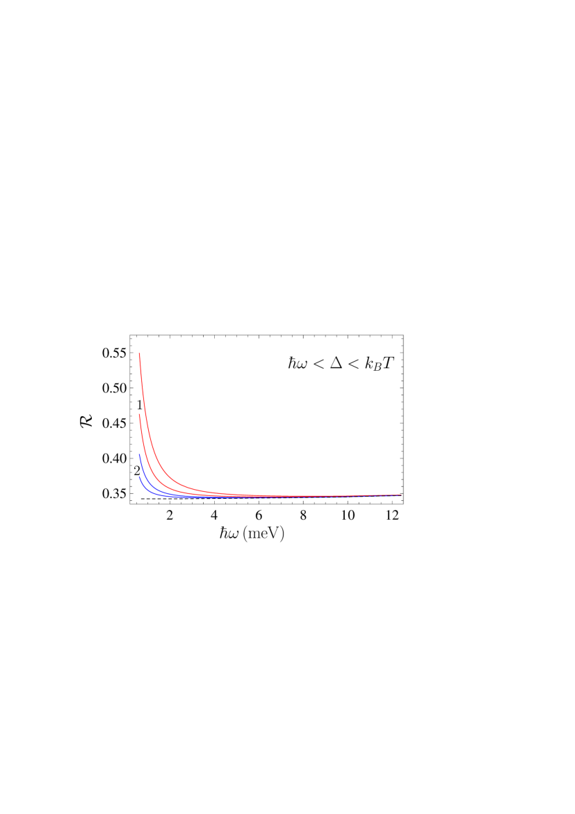
The computational results for the reflectances are presented in Fig. 1 as functions of frequency of the incident light. The pair of solid lines notated 1 shows reflectances of graphene-coated silica films which thicknesses are determined from the condition of maximum reflectance. The pair of solid lines notated 2 shows reflectances of a graphene-coated film which thickness is found from the condition of maximum reflectance (18) with no account of graphene. In each pair the top line is plotted for graphene with meV and the bottom line for graphene with meV. The dashed line demonstrates the maximum reflectance of an uncoated film. It is almost flat because in the frequency region considered has only minor dependence on .
As seen in Fig. 1, in the far-infrared region of the spectrum the presence of graphene coating significantly affects the maximum reflectance of a silica film. The largest impact is reached at meV. Here, the optimal film thickness is equal to m for meV and (the top line of pair 1). This should be compared with the optimal thickness m of an uncoated film leading to its maximum reflectance. The film of thickness , if coated with graphene, would have a reflectance of only . The maximum reflectance of an uncoated film is equal to . Thus, a relative increase in the maximum reflectance due to graphene coating in this frequency range is equal to 60%. This is reached by a relative increase of the optimal film thickness by 48%. The minimum reflectance of a graphene-coated film at meV is equal to . It is reached for a film of m thickness. This should be compared with and m. Note, however, that the transmittance of the film of thickness reaches 0.924, i.e., remains rather high.
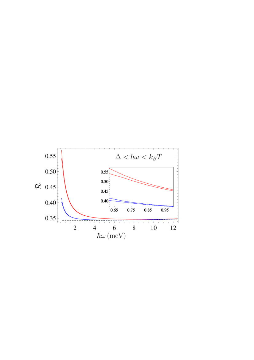
Next we consider the case when the width of the gap is smaller than all considered frequencies, i.e., (remind that at K). Although in this case , the inequalities and remain valid. Thus, in Eq. (27) and in Eq. (28) again ensure that the reflectances and reach the maximum and minimum values, respectively.
In Fig. 2 we present the computational results for the reflectances as functions of frequency. Similar to Fig. 1, the pair 1 of solid lines shows reflectances for the films of thickness and the pair 2 shows reflectances for the films of thickness found with no account of graphene. The top and bottom lines in each pair are for graphene coating with and 0.6 meV, respectively. The region of small frequencies is shown on an inset for better visualization. The dashed line is for an uncoated film.
As can be seen in Fig. 2, graphene coating with a smaller width of the band gap strongly affects the maximum reflectances although the impact of a specific value of is not so pronounced as in Fig. 1. Thus, for a gapless graphene coating at meV we have m and (the top line of pair 1). At the same time, if a graphene-coated film has the thickness m determined with no account of graphene we obtain the smaller value (the top line of pair 2). The maximum reflectance of an uncoated film in this case is reached for a film of thickness m. The resulting relative increase in the maximum reflectance due to the presence of graphene coating is equal to 66%. The respective relative change in the film thickness is by 50.1%. At meV the minimum reflectance of a graphene-coated film is reached for a film thickness m. For an uncoated film is reached for m. In this case the maximum transmittance is equal to 0.91.
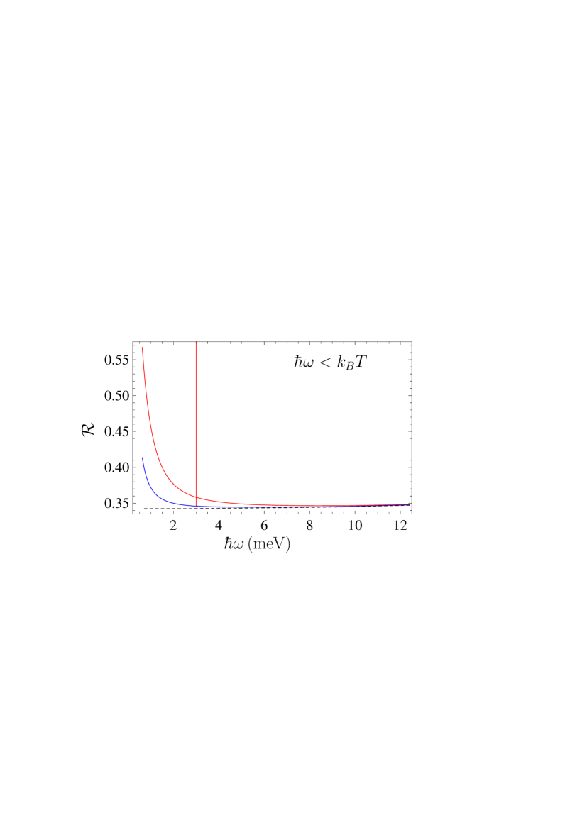
The last possibility, when is larger than in our frequency region but less than , remains to be investigated. Here, again, with exception of only a vicinity of frequency , where goes to . In the frequency region under consideration the width of this vicinity is unphysically narrow 26 . As a result, and in Eqs. (27) and (28) provide the maximum and minimum values to the reflectance of a graphene-coated film, respectively.
The computational results for the reflectances as functions of frequency are presented in Fig. 3. The top solid line shows the maximum reflectance of a SiO2 film coated by graphene with meV, where the optimal film thickness is determined with account of the graphene coating. The bottom solid line shows similar results but for a film thickness found with no account of graphene. As in Figs. 1 and 2, the dashed line reproduces the maximum reflectance of an uncoated film of thickness . As an example, for meV we have (the top line) and m. At the same frequency the maximum reflectance for a film of thickness m is equal to (the bottom line). In the absence of the graphene coating we again have . This leads to the maximum relative change of 65.6% due to the presence of graphene. The minimum reflectance is reached for a film thickness m. This corresponds to the transmittance of 91%. Note also the presence of the vertical peak at . It is caused by the break of continuity where goes to and, thus, . As mentioned above, this peak in the reflectance is unphysically narrow and only part of it is shown in Fig. 3.
IV Conclusions and discussion
In the foregoing, we have investigated the impact of graphene coating on the maximum and minimum reflectances of transparent optical films at normal incidence with account of multiple reflections. The general analytic expressions are found for the film thicknesses leading to the maximum and minimum reflectances in the presence of graphene. These results are determined by the index of refraction of film material (as for uncoated films in the commonly known classical case) and by the 00 component of the polarization tensor of graphene found recently in the framework of the Dirac model. Thus, the respective film thicknesses and the maximum and minimum reflectances and transmittances can now be calculated for any film material at any temperature using the developed formalism.
The obtained results were illustrated with the example of amorphous SiO2 films which are often used as the underlying substrates for graphene sheets (see, e.g., Refs. 40 ; 44 ). It has been known that in the application region of the Dirac model this material possesses two frequency regions of transparency belonging to the near-infrared and far-infrared domains of the spectrum. We have calculated both the maximum and minimum reflectances and respective film thicknesses for films coated with graphene with different values of the gap width and compared them with respective values for an uncoated film. According to our results, in the near-infrared domain graphene makes only a minor impact on the reflectance and transmittance of an uncoated film.
Quite to the opposite, it was shown that for frequencies belonging to the far-infrared domain graphene coating makes a profound effect on the maximum and minimum reflectances, and also on the thicknesses of films whereby these extremum values are reached. Here, we have considered three options depending on the relationship between the width of a graphene gap and the frequency. In all cases considered the relative increase of the maximum reflectance due to graphene coating is up to 65%. This is accompanied with up to 50% relative increase of the film thickness whereby the maximum reflectance is reached. It was shown also that the graphene-coated SiO2 film of appropriate thickness may possess a transmittance of more than 90%, i.e., for less than 10% smaller than that in the absence of graphene coating.
The obtained results are interesting not only for fundamental physics. At the present time graphene-coated films made of different materials find prospective technological applications in optoelectronic devices 45 ; 46 , corrosion protection 47 ; 48 , solar cells 49 ; 50 , transparent electrodes 51 , biosensors 52 , and in many others. These applications would require the greatest possible transmittance or reflectance of the graphene-coated films in use. The optical parameters of such films can be specified beforehand using the formalism developed.
Acknowledgments
The work of V.M.M. was partially supported by the Russian Government Program of Competitive Growth of Kazan Federal University.
References
- (1) M. I. Katsnelson, Graphene: Carbon in Two Dimensions (Cambridge University Press, Cambridge, 2012).
- (2) Physics of Graphene, ed. H. Aoki and M. S. Dresselhaus (Springer, Cham, 2014).
- (3) A. H. Castro Neto, F. Guinea, N. M. R. Peres, K. S. Novoselov, and A. K. Geim, The electronic properties of graphene, Rev. Mod. Phys. 81, 109 (2009).
- (4) N. M. R. Peres, The transport properties of graphene: An introduction, Rev. Mod. Phys. 82, 2673 (2010).
- (5) S. Das Sarma, S. Adam, E. H. Hwang, and E. Rossi, Electronic transport in two-dimensional graphene, Rev. Mod. Phys. 83, 407 (2011).
- (6) D. N. Basov, M. M. Fogler, A. Lanzara, Feng Wang, and Yuanbo Zhang, Colloquim: Graphene spectroscopy, Rev. Mod. Phys. 86, 959 (2014).
- (7) T. Stauber, N. M. R. Peres, and A. K. Geim, Optical conductivity of graphene in the visible region of the spectrum, Phys. Rev. B 78, 085432 (2008).
- (8) V. P. Gusynin, S. G. Sharapov, and J. P. Carbotte, Anomalous absorption line in the magneto-optical response of graphene, Phys. Rev. Lett. 98, 157402 (2007).
- (9) L. A. Falkovsky and S. S. Pershoguba, Optical far-infrared properties of a graphene monolayer and multilayer, Phys. Rev. B 76, 153410 (2007).
- (10) M. Auslender and M. I. Katsnelson, Generalized kinetic equations for charge carriers in graphene, Phys. Rev. B 76, 235425 (2007).
- (11) L. A. Falkovsky, Optical properties of graphene, J. Phys.: Conf. Series 129, 012004 (2008).
- (12) T. G. Pedersen, A.-P. Jauho, and K. Pedersen, Optical response and excitons in gapped graphene, Phys. Rev. B 79, 113406 (2009).
- (13) P. K. Pyatkovsky, Dynamical polarization, screening, and plasmons in gapped graphene, J. Phys.: Condens. Matter 21, 025506 (2009).
- (14) A. Scholz and J. Schliemann, Dynamical current-current susceptibility of gapped graphene, Phys. Rev. B 83, 235409 (2011).
- (15) C. A. Dartora and G. G. Cabrera, gauge invariance leading to charge and spin conductivity of Dirac fermions in graphene, Phys. Rev. B 87, 165416 (2013).
- (16) M. Merano, Fresnel coefficients of a two-dimensional atomic crystal, Phys. Rev. A 93, 013832 (2016).
- (17) D. Drosdoff and L. M. Woods, Casimir forces and graphene sheets, Phys. Rev. B 82, 155459 (2010).
- (18) D. Drosdoff and L. M. Woods, Casimir interaction between graphene sheets and metamaterials, Phys. Rev. A 84, 062501 (2011).
- (19) Bo E. Sernelius, Retarded interactions in graphene systems, Phys. Rev. B 85, 195427 (2012).
- (20) A. D. Phan, L. M. Woods, D. Drosdoff, I. V. Bondarev, and N. A. Viet, Temperature dependent graphene suspension due to thermal Casimir interaction, Appl. Phys. Lett. 101, 113118 (2012).
- (21) M. Bordag, I. V. Fialkovsky, D. M. Gitman, and D. V. Vassilevich, Casimir interaction between a perfect conductor and graphene described by the Dirac model, Phys. Rev. B 80, 245406 (2009).
- (22) I. V. Fialkovsky, V. N. Marachevsky, and D. V. Vassilevich, Finite-temperature Casimir effect for graphene, Phys. Rev. B 84, 035446 (2011).
- (23) M. Bordag, G. L. Klimchitskaya, V. M. Mostepanenko, and V. M. Petrov, Quantum field theoretical description for the reflectivity of graphene, Phys. Rev. D 91, 045037 (2015); 93, 089907(E) (2016).
- (24) M. Bordag, I. Fialkovskiy, and D. Vassilevich, Enhanced Casimir effect for doped graphene, Phys. Rev. B 93, 075414 (2016); 95, 119905(E) (2017).
- (25) G. L. Klimchitskaya and V. M. Mostepanenko, Conductivity of pure graphene: Theoretical approach using the polarization tensor, Phys. Rev. B 93, 245419 (2016).
- (26) G. L. Klimchitskaya and V. M. Mostepanenko, Quantum electrodynamic approach to the conductivity of gapped graphene, Phys. Rev. B 94, 195405 (2016).
- (27) G. L. Klimchitskaya, V. M. Mostepanenko, and V. M. Petrov, Conductivity of graphene in the framework of Dirac model: Interplay between nonzero mass gap and chemical potential, Phys. Rev. B 96, 235432 (2017).
- (28) G. L. Klimchitskaya, C. C. Korikov, and V. M. Petrov, Theory of reflectivity properties of graphene-coated material plates, Phys. Rev. B 92, 125419 (2015); 93, 159906(E) (2016).
- (29) G. L. Klimchitskaya and V. M. Mostepanenko, Reflectivity properties of graphene with nonzero mass-gap parameter, Phys. Rev. A 93, 052106 (2016).
- (30) G. L. Klimchitskaya and V. M. Mostepanenko, Optical properties of dielectric plates coated with gapped graphene, Phys. Rev. B 95, 035425 (2017).
- (31) M. Bordag, G. L. Klimchitskaya, and V. M. Mostepanenko, Thermal Casimir effect in the interaction of graphene with dielectrics and metals, Phys. Rev. B 86, 165429 (2012).
- (32) M. Chaichian, G. L. Klimchitskaya, V. M. Mostepanenko, and A. Tureanu, Thermal Casimir-Polder interaction of different atoms with graphene, Phys. Rev. A 86, 012515 (2012).
- (33) G. L. Klimchitskaya and V. M. Mostepanenko, Van der Waals and Casimir interactions between two graphene sheets, Phys. Rev. B 87, 075439 (2013).
- (34) K. Kaur, J. Kaur, B. Arora, and B. K. Sahoo, Emending thermal dispersion interaction of Li, Na, K and Rb alkali-metal atoms with graphene in the Dirac model, Phys. Rev. B 90, 245405 (2014).
- (35) G. L. Klimchitskaya, V. M. Mostepanenko, and Bo E. Sernelius, Two approaches for describing the Casimir interaction with graphene: density-density correlation function versus polarization tensor, Phys. Rev. B 89, 125407 (2014).
- (36) G. L. Klimchitskaya and V. M. Mostepanenko, Origin of large thermal effect in the Casimir interaction between two graphene sheets, Phys. Rev. B 91, 174501 (2015).
- (37) V. B. Bezerra, G. L. Klimchitskaya, V. M. Mostepanenko, and C. Romero, Nernst heat theorem for the thermal Casimir interaction between two graphene sheets, Phys. Rev. A 94, 042501 (2016).
- (38) G. Bimonte, G. L. Klimchitskaya, and V. M. Mostepanenko, How to observe the giant thermal effect in the Casimir force for graphene systems, Phys. Rev. A 96, 012517 (2017).
- (39) C. Henkel, G. L. Klimchitskaya, and V. M. Mostepanenko, Influence of chemical potential on the Casimir-Polder interaction between an atom and gapped graphene or graphene-coated substrate, Phys. Rev. A 97, 032504 (2018).
- (40) A. A. Banishev, H. Wen, J. Xu, R. K. Kawakami, G. L. Klimchitskaya, V. M. Mostepanenko, and U. Mohideen, Measuring the Casimir force gradient from graphene on a SiO2 substrate, Phys. Rev. B 87, 205433 (2013).
- (41) G. L. Klimchitskaya, U. Mohideen, and V. M. Mostepanenko, Theory of the Casimir interaction for graphene-coated substrates using the polarization tensor and comparison with experiment, Phys. Rev. B 89, 115419 (2014).
- (42) M. Born and E. Wolf, Pronciples of Optics (Cambridge University Press, Cambridge, 1999).
- (43) Handbook of Optical Constants of Solids, Vol. 2, edited by E. D. Palik (Academic, New York, 1991).
- (44) K. F. Mak, M. Y. Sfeir, Y. Wu, C. H. Lui, J. A. Misewich, and T. F. Heinz, Measurement of the optical conductivity of graphene, Phys. Rev. Lett. 101, 196405 (2008).
- (45) Yu. V. Bludov, M. I. Vasilevskiy, and N. M. R. Peres, Mechanism for graphene-based optoelectronic switches by turning surface plasmon-polariton in monolayer graphene, Europhys. Lett. 92, 68001 (2010).
- (46) K. Chung, C.-H. Lee, and G.-C. Yi, Transferable GaN layers grown on ZnO-coated graphene layers for optoelectronic devices, Science 330, 655 (2010).
- (47) R. K. S. Raman, P. Ch. Banerjee, D. E. Lobo, et. al., Protecting copper from electrochemical degradation by graphene coating, Carbon 50, 4040 (2012).
- (48) L. F. Dumée, L. He, Z. Wang, et. al., Growth of nano-textured graphene coatings across highly porous stainless steel supports towards corrosion resistant coatings, Carbon 87, 395 (2015).
- (49) W. Hong, Yu. Xu, G. Lu, Ch. Li, and G. Shi, Transparent graphene/PEDOT-PSS composite films as counter electrodes of dye-sensitized solar cells, Electrochem. Commun. 10, 1555 (2008).
- (50) Springer Handbook of Nanomaterials, edited by R. Vajtai (Springer, Berlin, 2013).
- (51) S. Watcharotone, D. A. Dikin, S. Stankovich, et. al., Graphene-silica composite thin films as transparent conductors, Nano Lett. 7, 1888 (2007).
- (52) T. Kuila, S. Bose, P. Khanra, A. K. Mishra, N. H. Kim, and J. H. Lee, Recent advances in graphebe-based biosensors, Biosens. Bioelectr. 29, 4637 (2011).