Conductance features of core-shell nanowires determined by the internal geometry
Abstract
We consider electrons in tubular nanowires with prismatic geometry and infinite length. Such a model corresponds to a core-shell nanowire with an insulating core and a conductive shell. In a prismatic shell the lowest energy states are localized along the edges (corners) of the prism and are separated by a considerable energy gap from the states localized on the prism facets. The corner localization is robust in the presence of a magnetic field longitudinal to the wire. If the magnetic field is transversal to the wire the lowest states can be shifted to the lateral regions of the shell, relatively to the direction of the field. These localization effects should be observable in transport experiments on semiconductor core-shell nanowires, typically with hexagonal geometry. We show that the conductance of the prismatic structures considerably differs from the one of circular nanowires. The effects are observed for sufficiently thin hexagonal wires and become much more pronounced for square and triangular shells. To the best of our knowledge the internal geometry of such nanowires is not revealed in experimental studies. We show that with properly designed nanowires these localization effects may become an important resource of interesting phenomenology.
I Introduction
The fabrication of various types of nanostructures allows for the design of systems with controllable properties of the electronic states. Amongst such systems are core-shell nanowires, which are radial heterojunctions of two, or even more, different semiconductor materials. Typically a central material (core) is surrounded by an outer layer (shell). The length of such nanowires is usually of the order of microns, whereas the diameter is between a few tens to a few hundreds of nanometers. An interesting aspect of this structure is the transversal geometry. Semiconductor core-shell nanowires, most often based on III-V materials, are almost always prismatic, and rarely cylindrical. The typical shape of the cross section is hexagonal Rieger et al. (2012); Blömers et al. (2013); Haas et al. (2013); Plochocka et al. (2013); Jadczak et al. (2014); Pemasiri et al. (2015). Interestingly, other prismatic geometries can also be achieved, like square Fan et al. (2006) or even triangular Qian et al. (2004, 2005); Baird et al. (2009); Heurlin et al. (2015); Dong et al. (2009); Yuan et al. (2015). The present art of manufacturing allows even for etching out the core and obtaining prismatic semiconductor nanotubes with vacuum inside Haas et al. (2013); Rieger et al. (2012).
In general, the specific geometry of the core-shell nanowires has not been studied much experimentally. It is either seen as a natural outcome, when the nanowires are hexagonal, or as a curiosity, when they are of different shapes. The main interest is rather related to the materials used, the quality of the nanowires (like defect free), a specific size of the core or the shell, specific length, etc. Still, in particular, the triangular wires showed very interesting features such as a broad range of emitted wavelengths at room temperature Qian et al. (2008, 2005) or diode characteristicsDong et al. (2009), but such properties were not really associated with the shape of the cross section and/or with particle localization. Remarkably, triangular nanowires possess intrinsic polarization effects that may break the three-fold geometric symmetry of the cross-section Wong et al. (2011).
Theoretically, the prismatic geometry of the nanowire, and especially of the shell itself, is a unique, and a very important feature, which can lead to very interesting and rich physics. If the materials, the geometry, the doping, and the shell thickness are properly adjusted, the shell becomes a tubular conductor with edges, and each edge may behave like a quasi-one-dimensional channel. A pioneer theoretical work has shown that carriers in prismatic shells can form a set of quasi-one-dimensional quantum channels localized at the prism edges Ferrari et al. (2009a). More recently it has been predicted that such a prismatic shell can host several Majorana states which may interact with each other Manolescu et al. (2017); Stanescu et al. (2018). Another recent prediction is that a magnetic field transversal to a tubular nanowire, either made of normal semiconductors, or of a topological insulator material, may induce the sign reversal of the electric current generated by a temperature gradient Erlingsson et al. (2017); Thorgilsson et al. (2017); Erlingsson et al. (2018).
In this paper we consider prismatic tubes as models of core-shell nanowires with an insulating core and a conductive shell. Our models are also applicable to uniform nanowires (i.e. not core-shell) which have conductive surface states due to the Fermi level pinning Heedt et al. (2016). However, we are not addressing the nanowires built from topological materials, but we use in our calculations a Schrödinger Hamiltonian. In our models the cross section of the prismatic shell is a narrow polygonal ring (hexagonal, square, or triangular), i.e., with lateral thickness much smaller than the overall diameter of the nanowire.
In this geometry the electrons with the lowest energies are localized in the corners of the polygon and the electrons in the next layer of energy states are localized on the sides Bertoni et al. (2011); Royo et al. (2013, 2014, 2015); Fickenscher et al. (2013); Shi et al. (2015). The corner and side states are energetically separated by an interval that depends on the geometry and on the aspect ratio of the polygon, it increases with decreasing the shell thickness or the number of corners, and it can become comparable or larger than the energy corresponding to the room temperature Sitek et al. (2015, 2016a). Hence, such structures can contain a well-separated subspace of corner states, with sharp localization peaks, and potentially robust to many types of perturbations. On the contrary, if the shell is relatively thick with respect to the diameter of the wire, the corner localization broadens and the polygonal structure has less effect on the electron distribution Sitek et al. (2016b).
To the best of our knowledge, experimental results with features related to the internal geometry of the nanowire do not exist, or are very rare. One investigation, using inelastic light scattering, indicated the coexistence of one- and two-dimensional electron channels, along the edges and facets, respectively, of GaAs core-shell nanowires Funk et al. (2013). In transport experiments one can mention here the detection of flux periodic oscillations of the conductance in the presence of a magnetic field longitudinal to the nanowire Gül et al. (2014), which indicates the radial localization of the electrons in the shell. Or, flux periodic oscillations with the magnetic field perpendicular to the nanowire, due to the formation of snaking states on the sides of the tubular conductor Heedt et al. (2016); Manolescu et al. (2016). Nevertheless, experimental results indicating the presence of corner or side localized states, or the energy gap between them, or other details implied by the prismatic geometry of the shell, are not reported.
The intention of this paper is to predict specific features of the conductance of core-shell nanowires when the electronic transport occurs within the shell, determined by the prismatic geometry of the nanowire. Such features, which could be experimentally tested, can reveal to what extent the electronic states are influenced by the polygonal geometry, and if not, to what extent the quality of the nanowire needs to be improved in order to achieve a robust corner localization.
Next, in Section II we describe our model and methodology, in Section III we discuss the transverse modes and the expected conductance steps, in Section IV we consider a magnetic field longitudinal to the nanowire, in Section V a perpendicular magnetic field and finally in Section VI we summarize the conclusions.
II Model and methods
We analyze a system of non-interacting electrons, confined in a prismatic shell with polygonal cross section, in the presence of a uniform magnetic field . The axes and are chosen perpendicular to the shell and the axis is longitudinal. The Hamiltonian can be decomposed as
| (1) |
where the terms , , and correspond to the transverse, the longitudinal, and the spin degrees of freedom, respectively.
The transverse Hamiltonian is,
| (2) |
where is the effective electron mass in the shell material, is the vector potential, and is an external electric field perpendicular to the wire. The transverse Hamiltonian depends only on the longitudinal magnetic field .
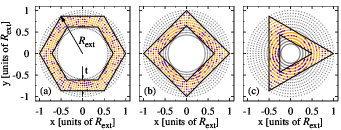
Technically, the Hamiltonian (2) is restricted to a lattice of points that covers the cross section of the shell. In order to define the lattice we begin with a circular disk which is discretized in polar coordinates Daday et al. (2011). Next, we enclose the polygonal shell within this area and exclude all lattice points situated outside the shell, as shown in Fig. 1. This method allows us to describe both symmetric and non-symmetric polygonal shells without the need of adapting the background grid geometry to the specific polygon or redefining Hamiltonian matrix elements Sitek et al. (2015, 2016a). As a second method we also used the Kwant software Groth et al. (2014) and obtained the same numerical results for the matrix elements, this time using a triangular grid.
The longitudinal Hamiltonian is
| (3) |
which depends on the magnetic field transverse to the nanowire , which can be chosen at different angles relatively to the corners or sides of the shell.
And finally the spin Hamiltonian is
| (4) |
where is the effective g factor, is Bohr’s magneton, denote the Pauli matrices, and is the total magnetic field.
In our numerical calculations we first calculate the eigenstates of the transverse Hamiltonian, (), and obtain the corresponding eigenvectors in the position representation, , where , is the localization probability on the lattice site . Next, we retain only a set of low-energy transverse modes, and together with the plane waves in the direction , being the wave vector and the (infinite) length of the nanowire, and with the spin states , we form a basis in the Hilbert space of the total Hamiltonian, . In the absence of the magnetic field transverse to the wire (), the kets are eigenvectors of the total Hamiltonian, with eigenvalues . If the transverse motion becomes dependent on , and then we diagonalize the total Hamiltonian for a discretized series of values, to obtain its eigenvalues (), and its eigenvectors expanded in the basis .
The next step of our calculations is to evaluate the electric current along the nanowire in the presence of a voltage bias. The operator describing the contribution of an electron which is localized at point , to the total charge-current density observed in a spatial point , is defined as
where is the particle-density operator and the velocity operator Messiah (1999). In our case we need only the component along the nanowire, . We can define the expected value of the total charge current flowing in the positive or negative direction along the nanowire (i.e. in the direction) as
| (5) |
The integration is performed over the cross section of the shell, practically as a summation over all lattice sites , whereas the scalar product included in the square brackets is an integration over the electrons position . represents the Fermi function, is the temperature, and Boltzmann’s constant. Here are the chemical potentials associated with electrons having positive or negative velocity along the nanowire. Obviously, in equilibrium the corresponding currents compensate each other and the total current is zero.
To generate a current along the nanowire we create an imbalance between the states with positive velocity, i.e., , and negative velocity, i.e., , by considering in Eq. (5) different chemical potentials, and , respectively. The current is thus driven along the nanowire by the potential bias . This procedure, well established in ballistic transport theory Datta (1997), allows us to calculate the characteristic and the conductance in the small bias limit.
To include the effect of disorder on the conductance we consider a nanowire with a scattering region of a finite length containing a random distribution of impurities, and we assume elastic electron-impurity collisions. In this case the impurities can be represented by an extra random term in the total Hamiltonian (1). The current and the conductance can be calculated using the well known concept of transmission function. Here we compute the transmission function by using the Fisher-Lee formula Fisher and Lee (1981) and the recursive Green’s function method Ferry and Goodnick (1997). A summary of the method for cylindrical geometry can be found in Ref. Erlingsson et al. (2017) (Supplemental Material).
We also address in our paper the case of a long nanowire, much longer than the scattering length, when the transport is far from ballistic. In principle this case can be treated with the recursive Green’s functions method, by including a large number of impurities, but it becomes computationally very expensive. As an alternative approach we will consider in this case a nanowire of infinite length, and we will use the traditional Kubo formula, which allows one to calculate the conductivity by performing a statistical average over impurity configurations Doniach and Sondheimer (1998):
| (6) |
where is the volume of the conductor and is the spectral function which represents the broadening of the energy level due to the disorder. In this study we model the spectral function for each energy level as a Gaussian function,
| (7) |
whose width parameter represents the disorder energy. This model of spectral function was used in the past for describing the impurity effects in the two-dimensional electron gas Ando et al. (1982), but also more recently to incorporate the effect of the electrodes on the density of states in molecular nanowires Tada et al. (2004).
In the next sections we will show results for the conductance of core-shell nanowires, related to their internal geometry, in different situations, using the computational methods mentioned above.
III Transverse modes for zero magnetic field
In all the following examples the external radius of the polygonal shell, which is the distance from the center to one corner, as indicated in Fig. 1(a), is nm, whereas the side thickness varies between 2-8 nm. The numerical calculations were performed for InAs bulk parameters, which are ( being the electron mass of a free electron), and .
Because of the polygonal cross section of the shell the lowest transverse modes are localized in the corners of the polygons while the probability distributions corresponding to higher modes have maxima on the sides Sitek et al. (2015), as illustrated in Fig. 2. In three dimensions the corner states form 1D conductive channels along the edges of the prismatic shell Shi et al. (2015). For each polygon there are corner states, where is the number of corners (or sides) and the factor 2 accounts for the spin. The energy dispersion of corner states decreases with the number of corners. For example, for nm shell thickness these states fit into the intervals of 15.3 meV for the the hexagon, 3.1 meV for the square, and 0.2 meV for the triangle (measured from the ground state). For each geometry, above the group of corner states, there is another group of states, localized on the the sides of the polygons (the lower part of Fig. 2). For the present radius (30 nm) and side thickness (6 nm) the energy dispersion within each group of corner and side states is exceeded by the energy interval (or gap) between these groups, which are meV for hexagon, meV for square and meV for triangle.

These energy gaps make a big difference between a polygonal and a cylindrical shell. In the latter case, if , one expects the transverse energies , with the quantum number of the angular momentum, i.e., with energy intervals uniformly increasing as . In addition, in the cylindrical case (not shown in Fig. 2), at zero magnetic field, the transverse modes are four fold degenerate, both spin and orbital, except the ground state which is only two fold, spin degenerate. For symmetric polygons, because of the reduced, discrete symmetry, the orbital degeneracy is lifted between consecutive groups of transverse states. In particular, for symmetric shells, the sequence of degeneracy orders (2-fold or 4-fold) of the corner/side states, with increasing the energy, is 2442/2442 for the hexagon, 242/242 for the square, and 24/42 for the triangle.
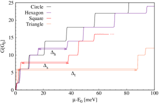
In Fig. 3 we compare the conductance steps expected in the cylindrical and in the three prismatic geometries, when the chemical potential is varied. Here we assume ballistic transport and symmetric shells. The conductance is derived with Eq. (5), using a small bias and temperature K. The steps obtained for circular and hexagonal structures are visibly different, with a extra plateau at for the hexagon, () corresponding to the gap between corner and side states. These plateaus increase dramatically for the triangular and square geometries, at and at , respectively. For the hexagonal shell the corner states are visible as steps at , , and , similar to the circular case. For the square, instead, we see only some shoulders indicating the corner states at and , and for the triangular case they are not resolved.
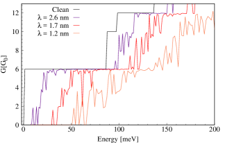
In order to obtain the conductance of a nanowire with impurities we consider scattering centers, with random characteristic energy between 0 and 0.5 meV, at random locations within the tubular nanowire. We calculate the conductance, this time with the recursive Green’s function approach, for the example of the triangular geometry, at zero temperature. The results are shown in Fig. 4 for a nanowire of 54.2 nm length with different impurity concentrations corresponding to a mean distance between the nearest neighbors of 2.7 nm, 1.6 nm and 1.2 nm. The impurity configurations are fixed in these cases, such that this situation corresponds to a specific mesoscopic sample with individual randomness. The impurity concentration is increased until the largest plateau, corresponding to the gap between the corner and side states, becomes nearly indistinguishable. This impurity concentration can offer a hint on how dirty a nanowire can be such that the conductance steps cannot be detected in the experiments.
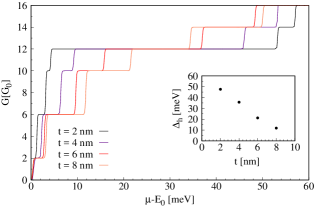
We now return to the clean nanowire to discuss the effect of the side thickness on the hexagonal geometry. With the parameters used in Fig. 3 the plateaus corresponding to side modes, i.e. above , are comparable or larger than . However, the relative magnitude of the energy intervals, i.e., of relatively to the dispersion of the corner and side states, increases with reducing the aspect ratio of the polygon, i.e., Sitek et al. (2016a). As a result, with reducing the thickness parameter , while is kept constant, the plateau at the transition between corner and side states becomes much more prominent. At the same time, the ratio between and the other energy intervals rapidly increases such that the plateaus in the corner domain become negligible relatively to the main one of width , as shown in Fig. 5.
In these examples we assumed the geometric symmetry of the nanowires. Nevertheless, shells with perfect polygonal symmetry cannot be fabricated, such that the symmetric case should be considered only for reference. Geometric imperfections, random impurities, or external electric fields (gates) remove the orbital degeneracies. In order to account for asymmetry we consider an electric field transversal to the wire, included in Eq. 2. In practice, this is a way to model also the effect of a lateral gate attached to the nanowire, or of the substrate where the nanowire is situated, typically used to control the carrier concentration with a voltage Sitek et al. (2015). Assuming this voltage is not very large, such that the electrons are still distributed over the entire shell (and not simply crowded near the gate), new plateaus can be obtained between the split orbital states, as shown in Fig. 6, where we compare the results obtained for a cylindrical and a hexagonal nanowire.
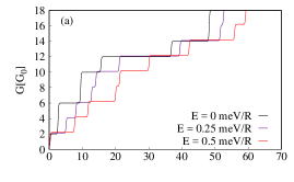
The electric field changes the electron density distribution by favoring some corner or sides over the others, depending on its orientation. This allows for the controllability of the electron localization within the shell. Although the first plateaus are similar for both the cylindrical and the hexagonal case the main difference arises from the orbital degeneracy pattern of the hexagonal nanowire, which is split at , separating corner from side states (2442/2442). It is also interesting to observe that, in the cylindrical nanowire, the electric field applied needs to be progressively stronger in order to split the orbital degeneracy of higher energy levels, as shown in Fig. 6(b). Additionally, for the hexagonal wire, rotating the direction of the electric field leads to a change in the secondary plateaus but leaves the main one (at ) unaffected (not shown).
IV Effects of a longitudinal magnetic field
We consider now a magnetic field in Eq. (2), longitudinal to the nanowire and its effects on the transverse modes. For a circular nanowire with a periodic energy spectrum vs. the magnetic field is expected, with period of one flux quantum in the cross sectional area. Such flux-periodic oscillations, related to the Aharonov-Bohm interference, have been observed experimentally on InAs/GaAs hexagonal core-shell nanowires with nm and nm Gül et al. (2014). The oscillations had additional modulations that were attributed to impurities, or subsequently to the spin splitting, by using a circular nanowire model of zero thickness Rosdahl et al. (2014).
Indeed, the presence of the spin disturbs or breaks the flux periodicity of the transverse modes when the magnetic field increases, as seen in Fig. 7(a) for a circular shell. In addition, the flux periodicity is also disturbed by the shell thickness. Flux periodic energy spectra for thin polygonal shells, without spin effects, have already been obtained by other authors Ferrari et al. (2009b, a); Ballester et al. (2013).
In Fig. 7(b) we show the energies of the transverse modes for our hexagonal shell. The energy gap between the corner and side states decreases when the magnetic field is increased, but, remarkably, still a large value survives at high magnetic fields, in our case above 10 T. The reason is that the orbital energy of the states localized in corners is significantly reduced compared to states of higher energies, an effect that becomes more pronounced in the square geometry, Fig. 7(c). In fact, the differences reveal the symmetry reduction from circular to hexagonal or square shapes. In these examples the orbital degree of freedom of the corner states is provided by their mutual coupling via tunneling across the polygon sides. Instead, in the triangular case, where the corner localization is the strongest, the tunneling is suppressed, and the orbital motion of the corner states is completely frozen, such that only the spin Zeeman energy is observable for the corner states in Fig. 7(d). The same can also happen for thinner square and hexagonal shells.
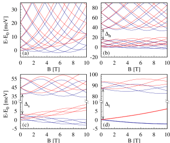
The conductance steps expected in the presence of a longitudinal magnetic field would develop according to the evolution of the transverse modes when increasing the field, by lifting both spin and orbital degeneracies. It is worth noting that, up to 10 T, the gap separating corner and side states prevails for the three polygonal shells, with the geometric parameters used, and that a new gap separating the corner states with different spin is created as a consequence of the Zeeman splitting for the triangular and square nanowires, where the orbital degree of freedom is most restricted.
V Effects of a magnetic field perpendicular to the nanowire
V.1 Charge and current distributions
A magnetic field orthogonal to the nanowire axis, which can be incorporated in the longitudinal Hamiltonian, Eq. (3), creates a second localization mechanism, in addition to the localization imposed by the polygonal geometry. This type of magnetic localization has been studied in recent years for the cylindrical shell geometry by several authors Tserkovnyak and Halperin (2006); Bellucci and Onorato (2010); Manolescu et al. (2013); Rosdahl et al. (2015); Chang and Ortix (2017). If the electrons are confined on a cylindrical surface, their orbital motion is governed by the radial component of the magnetic field. Assuming a magnetic field uniform in space, its radial component vanishes and changes sign along the two parallel lines on the cylinder situated at angles relatively to the direction of the field, and if the field is strong enough the electrons have snaking trajectories along these lines. At the same time, at angles and the electrons perform closed cyclotron loops. This localization mechanism leads to an accumulation of electrons on the sides of the cylinder, where the snaking states are formed, and to the depletion the regions hosting the cyclotron orbits Manolescu et al. (2013).
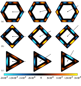
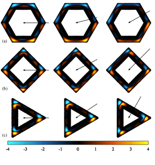
In a thin prismatic shell the geometric and magnetic localization of the electrons coexist. Therefore, the distribution of electrons is expected to depend on the orientation of the magnetic field relatively to the prism edges or facets, as in the examples shown in Fig. 9. Here we consider a carrier concentration of as reported in the recent literature Heedt et al. (2016). In each case the color scale represents the difference between the carrier concentration at T and at for the three geometries. With the present parameters these differences are somewhere up to 10%. Furthermore, for each geometry, the local changes of the density when the angle of the magnetic field is varied, are up to 1% only. Still, as we shall see, this variation should be sufficient to have implications on the transport data.
Next, in Fig. 9 we show the current distributions in the equilibrium states, i.e. in the absence of a biased chemical potential (). In the absence of the magnetic field the current distribution is zero everywhere in the shell, i.e. the positive currents and negative currents compensate in each point. In the presence of the magnetic field, as expected, the Lorentz force may create local currents, as shown in the figure, which no longer compensate locally, but indeed the integrated current is zero. The local currents are in fact loops along the axis of the nanowire, closing up at infinity. Still, it is interesting to observe the compensation of these loops. In the cases where the magnetic field points along the direction of one of the symmetry axes of the cross section the loops are compensated, with the same current flowing in both directions, and the channels are paired with the ones on the opposite side of the geometric symmetry axis relative to the magnetic field direction. The pairing can happen within the same corner or side or on opposite ones. In the cases where the magnetic field does not point along one of the symmetry axes the loops are no longer compensated and the current traveling in both directions is not the same. Instead, the compensation occurs when adding the loop on the opposite side of the shell.
V.2 Energy spectra and conductivity
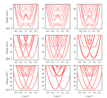
The energy dispersion with respect to the wave vector , corresponding to the situations shown in Figs. 9 and 9, can be seen in Fig. 10. The dashed horizontal lines indicate the chemical potential corresponding to the selected carrier concentration. In all cases, in the absence of the magnetic field the position of the chemical potential is somewhere at the level of the side states. The presence of the magnetic field mixes the corner and the side states and leads to quite complex changes in the spectra and in the charge or current distributions. And, as we can see, the energy dispersions are also sensitive to the orientation of the field relatively to the prismatic shell.
Note that, in the triangular case, the spectra may not be symmetric (even) functions of the wave vector if the magnetic field is not aligned with a symmetry axis of the shell, like in the second example of Fig. 10(c), corresponding to the second example of Figs. 9(c) and 9(c). In this case the magnetic field is parallel to the side of the triangle. The sign reversal of the magnetic field leads to the sign reversal of the wave vector, i.e., to the same energy spectrum. The reason for the asymmetric spectra is that the triangular geometry is somehow special, compared to the hexagonal or square, because of the absence of an inversion center.
According to these results we can predict that due to the internal geometry of the nanowire the conductance should depend on the orientation of the magnetic field in a manner that indicates the polygonal cross section of the shell. We demonstrate this in Fig. 11 where we show the results obtained with the Kubo formula (6). In these calculations we assume infinitely long nanowires and we include a disorder broadening of the energy spectra described by the parameter meV in Eq. (7), i.e., we are far from the ballistic regime. In addition we consider temperatures up to 50 K, to emphasize that the conductance anisotropy should be also robust to thermal perturbations.
For each geometry the zero angle is considered when the field is oriented towards a prism edge, as shown in the first column of Fig. 9. The angular period of the conductivity, when the magnetic field rotates, is obtained when the magnetic field points to the next corner for the hexagon and square, i.e. and , respectively, whereas for the triangle it corresponds to a half of it, i.e. . Obviously, all figures can be continued by periodicity, up to a complete rotation of the magnetic field.
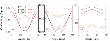
The conductivity described by the Kubo formula is, in this case, an example of band conductivity, i.e., it is directly related to the velocity of carriers along the transport direction, like in the ballistic case, and decreases when the disorder parameter increases Manolescu and Gerhardts (1997). The dependence on the temperature is more complicated. In this calculations we completely ignored the dependence on the temperature of the collisional broadening parameter , which is a separate problem. In our model the main effect of increasing the temperature is the population/depopulation of the states above/below the chemical potential, respectively, and to a lesser extent the variation of the chemical potential itself. Because the energy curves are nonlinear functions of the wave vector, Fig. 10, the velocity distribution of the carriers changes in a nonuniform manner, such that our conductivity may either increase or decrease with increasing the temperature. The relative variation of the conductivity with the angle is also not simple, meaning that it can increase or decrease, depending on how the energy spectra behave around the chemical potential when the magnetic field is changing orientation. In our examples we can see that the variation is the weakest for the triangular case, which is because the corner localization is stronger and their mixing with the side states is relatively weak.
The conductance anisotropy in hexagonal core-shell nanowires was already predicted for the case with electrons localized in the core Royo et al. (2013), but only in the ballistic regime, at much higher magnetic fields, and much less pronounced. In our case the results obtained in the ballistic regime are qualitatively similar to those shown in Fig. 11, except at low temperatures, when the conductance depends critically on the number of intersections of the Fermi energy with the energy bands, which may vary discontinuously. But, since it is difficult to obtain the ballistic regime in realistic experimental samples, our results show that the anisotropy of the shell could be easier resolved, in well attainable experimental conditions, and possibly not only at low temperatures.
V.3 Nonlinear I-V characteristics
Another indication of the internal geometry of the prismatic shell can be found in the characteristic, as we show in Fig. 12. The characteristics are obtained following the same method used for the conductance, i.e. Eq. (5). This time we create an imbalance between states with positive and negative velocity by increasing the potential bias far from the linear regime, starting with a chemical potential close to the lowest band bottom.
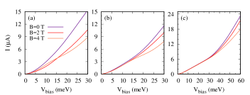
We first notice the bias threshold where the linear regime breaks. That is the lowest for the hexagonal geometry, below 5 meV, whereas for the square and triangular cases it increases to 15 meV and 35 meV, respectively. The change of slope of the curves, more clearly seen for square and triangular cases, indicate the transition from corner states to side states, as more channels are crossed, and could offer a possibility to observe experimentally the existence of the gap separating these groups of states. In some cases the magnetic field yields a reduction in energy and a shift in k-space of two mixed-spin bands, leading to an avoided crossing at . In these cases an inflection point is observed, more clearly for the hexagonal and square cases, as a consequence of the reduction in the number of levels crossed by the potential bias.
In the results shown in Fig. 12 we used a temperature of 25 K in order to increase the population of the states above the chemical potential. The curves were obtained assuming an infinite wire without impurities. To a first approximation their averaged effect can be incorporated in Eq. (5) by the substitution
In this way we could obtain results similar to those shown in Fig. 12 with a lower temperature, K, but with a disorder energy meV.
VI Conclusions
We presented several features of the conductance of core-shell nanowires with a conductive shell and an insulating core, which are consequences of the internal geometry of such nanowires, and can be probed in well achievable experimental conditions. The motivation of our work is to stimulate the interest of the experimental groups to do such investigations and to achieve the corresponding quality of the samples with a clear manifestation of the internal geometry.
Most of the presented results are basically determined by the energy spectra and by the geometric localization of the electrons. In the ballistic cases, with no impurities, there is no real need for transport calculations, the conductance can be obtained by simply counting the transverse modes. The transport calculations that we performed were intended to support the predictions from the spectra, in a qualitative manner. We used the transmission function for short, ballistic or quasi-ballistic wires, and Kubo formula for long (infinite) non-ballistic wires.
One of the most interesting aspects is that the states localized along the edges and those localized on the facets can be separated by a large energy gap, robust to many kinds of perturbations, such that a single core-shell nanowire may possibly function like a collection of thinner nanowires. Another interesting result is that the localization, and thus the conductance features, can be modified or controlled by external electric or magnetic fields.
Acknowledgements.
Instructive discussions with Patrick Zellekens, Thomas Schäpers, and Mihai Lepsa are highly appreciated. This work was supported by the Icelandic Research Fund.References
- Rieger et al. (2012) T. Rieger, M. Luysberg, T. Schäpers, D. Grützmacher, and M. I. Lepsa, Nano Letters 12, 5559 (2012).
- Blömers et al. (2013) C. Blömers, T. Rieger, P. Zellekens, F. Haas, M. I. Lepsa, H. Hardtdegen, Ö. Gül, N. Demarina, D. Grützmacher, H. Lüth, and T. Schäpers, Nanotechnology 24, 035203 (2013).
- Haas et al. (2013) F. Haas, K. Sladek, A. Winden, M. von der Ahe, T. E. Weirich, T. Rieger, H. Lüth, D. Grützmacher, T. Schäpers, and H. Hardtdegen, Nanotechnology 24, 085603 (2013).
- Plochocka et al. (2013) P. Plochocka, A. A. Mitioglu, D. K. Maude, G. L. J. A. Rikken, A. Granados del Águila, P. C. M. Christianen, P. Kacman, and H. Shtrikman, Nano Letters 13, 2442 (2013).
- Jadczak et al. (2014) J. Jadczak, P. Plochocka, A. Mitioglu, I. Breslavetz, M. Royo, A. Bertoni, G. Goldoni, T. Smolenski, P. Kossacki, A. Kretinin, H. Shtrikman, and D. K. Maude, Nano Letters 14, 2807 (2014).
- Pemasiri et al. (2015) K. Pemasiri, H. E. Jackson, L. M. Smith, B. M. Wong, S. Paiman, Q. Gao, H. H. Tan, and C. Jagadish, Journal of Applied Physics 117, 194306 (2015).
- Fan et al. (2006) H. Fan, M. Knez, R. Scholz, K. Nielsch, E. Pippel, D. Hesse, U. Gösele, and M. Zacharias, Nanotechnology 17, 5157 (2006).
- Qian et al. (2004) F. Qian, Y. Li, S. Gradečak, D. Wang, C. J. Barrelet, and C. M. Lieber, Nano Letters 4, 1975 (2004).
- Qian et al. (2005) F. Qian, S. Gradečak, Y. Li, C.-Y. Wen, and C. M. Lieber, Nano Letters 5, 2287 (2005).
- Baird et al. (2009) L. Baird, G. Ang, C. Low, N. Haegel, A. Talin, Q. Li, and G. Wang, Physica B: Condensed Matter 404, 4933 (2009).
- Heurlin et al. (2015) M. Heurlin, T. Stankevič, S. Mickevičius, S. Yngman, D. Lindgren, A. Mikkelsen, R. Feidenhans’l, M. T. Borgstöm, and L. Samuelson, Nano Letters 15, 2462 (2015).
- Dong et al. (2009) Y. Dong, B. Tian, T. J. Kempa, and C. M. Lieber, Nano Letters 9, 2183 (2009).
- Yuan et al. (2015) X. Yuan, P. Caroff, F. Wang, Y. Guo, Y. Wang, H. E. Jackson, L. M. Smith, H. H. Tan, and C. Jagadish, Adv. Funct. Mater. 25, 5300 (2015).
- Qian et al. (2008) F. Qian, Y. Li, S. Gradecak, H.-G. Park, Y. Dong, Y. Ding, Z. L. Wang, and C. M. Lieber, Nat Mater 7, 701 (2008).
- Wong et al. (2011) B. M. Wong, F. Léonard, Q. Li, and G. T. Wang, Nano Letters 11, 3074 (2011).
- Ferrari et al. (2009a) G. Ferrari, G. Goldoni, A. Bertoni, G. Cuoghi, and E. Molinari, Nano Letters 9, 1631 (2009a).
- Manolescu et al. (2017) A. Manolescu, A. Sitek, J. Osca, L. Serra, V. Gudmundsson, and T. D. Stanescu, Phys. Rev. B 96, 125435 (2017).
- Stanescu et al. (2018) T. D. Stanescu, A. Sitek, and A. Manolescu, Beilstein Journal of Nanotechnology 9, 1512 (2018).
- Erlingsson et al. (2017) S. I. Erlingsson, A. Manolescu, G. A. Nemnes, J. H. Bardarson, and D. Sanchez, Phys. Rev. Lett. 119, 036804 (2017).
- Thorgilsson et al. (2017) G. Thorgilsson, S. I. Erlingsson, and A. Manolescu, Journal of Physics: Conference Series 906, 012021 (2017).
- Erlingsson et al. (2018) S. I. Erlingsson, J. H. Bardarson, and A. Manolescu, Beilstein Journal of Nanotechnology 9, 1156 (2018).
- Heedt et al. (2016) S. Heedt, A. Manolescu, G. A. Nemnes, W. Prost, J. Schubert, D. Grützmacher, and T. Schäpers, Nano Letters 16, 4569 (2016).
- Bertoni et al. (2011) A. Bertoni, M. Royo, F. Mahawish, and G. Goldoni, Phys. Rev. B 84, 205323 (2011).
- Royo et al. (2013) M. Royo, A. Bertoni, and G. Goldoni, Phys. Rev. B 87, 115316 (2013).
- Royo et al. (2014) M. Royo, A. Bertoni, and G. Goldoni, Phys. Rev. B 89, 155416 (2014).
- Royo et al. (2015) M. Royo, C. Segarra, A. Bertoni, G. Goldoni, and J. Planelles, Phys. Rev. B 91, 115440 (2015).
- Fickenscher et al. (2013) M. Fickenscher, T. Shi, H. E. Jackson, L. M. Smith, J. M. Yarrison-Rice, C. Zheng, P. Miller, J. Etheridge, B. M. Wong, Q. Gao, S. Deshpande, H. H. Tan, and C. Jagadish, Nano Letters 13, 1016 (2013).
- Shi et al. (2015) T. Shi, H. E. Jackson, L. M. Smith, N. Jiang, Q. Gao, H. H. Tan, C. Jagadish, C. Zheng, and J. Etheridge, Nano Letters 15, 1876 (2015).
- Sitek et al. (2015) A. Sitek, L. Serra, V. Gudmundsson, and A. Manolescu, Phys. Rev. B 91, 235429 (2015).
- Sitek et al. (2016a) A. Sitek, G. Thorgilsson, V. Gudmundsson, and A. Manolescu, Nanotechnology 27, 225202 (2016a).
- Sitek et al. (2016b) A. Sitek, G. Thorgilsson, V. Gudmundsson, and A. Manolescu, Proceedings of the 18th International Conference on Transparent Optical Networks, (ICTON 2016) (2016b), doi: 10.1109/ICTON.2016.7550580.
- Funk et al. (2013) S. Funk, M. Royo, I. Zardo, D. Rudolph, S. Morkötter, B. Mayer, J. Becker, A. Bechtold, S. Matich, M. Döblinger, M. Bichler, G. Koblmüller, J. J. Finley, A. Bertoni, G. Goldoni, and G. Abstreiter, Nano Letters 13, 6189 (2013).
- Gül et al. (2014) O. Gül, N. Demarina, C. Blömers, T. Rieger, H. Lüth, M. I. Lepsa, D. Grützmacher, and T. Schäpers, Phys. Rev. B 89, 045417 (2014).
- Manolescu et al. (2016) A. Manolescu, G. A. Nemnes, A. Sitek, T. O. Rosdahl, S. I. Erlingsson, and V. Gudmundsson, Phys. Rev. B 93, 205445 (2016).
- Daday et al. (2011) C. Daday, A. Manolescu, D. C. Marinescu, and V. Gudmundsson, Phys. Rev. B 84, 115311 (2011).
- Groth et al. (2014) C. W. Groth, M. Wimmer, A. R. Akhmerov, and X. Waintal, New Journal of Physics 16, 063065 (2014).
- Messiah (1999) A. Messiah, Quantum Mechanics, Vol. I, Ch. X, p. 372 (Dover Publications, 1999).
- Datta (1997) S. Datta, Electronic Transport in Mesoscopic Systems (Cambridge University Press, 1997).
- Fisher and Lee (1981) D. Fisher and P. Lee, Phys. Rev. B 23, 6851 (1981).
- Ferry and Goodnick (1997) D. K. Ferry and S. M. Goodnick, Transport in Nanostructures, edited by H. Ahmed, M. Pepper, and A. Broers (Cambridge University Press, Cambridge, 1997).
- Doniach and Sondheimer (1998) S. Doniach and E. H. Sondheimer, Green’s Functions for Solid State Physicists (Imperial College Press, London, 1998).
- Ando et al. (1982) T. Ando, A. B. Fowler, and F. Stern, Rev. Mod. Phys. 54, 437 (1982).
- Tada et al. (2004) T. Tada, M. Kondo, and K. Yoshizawa, The Journal of Chemical Physics 121, 8050 (2004).
- Rosdahl et al. (2014) T. O. Rosdahl, A. Manolescu, and V. Gudmundsson, Phys. Rev. B 90, 035421 (2014).
- Ferrari et al. (2009b) G. Ferrari, C. Cuoghi, A. Bertoni, G. Goldoni, and E. Molinari, J.Phys.: Conf. Ser. 193, 012027 (2009b).
- Ballester et al. (2013) A. Ballester, C. Segarra, A. Bertoni, and J. Planelles, EPL (Europhysics Letters) 104, 67004 (2013).
- Tserkovnyak and Halperin (2006) Y. Tserkovnyak and B. I. Halperin, Phys. Rev. B 74, 245327 (2006).
- Bellucci and Onorato (2010) S. Bellucci and P. Onorato, Phys. Rev. B 82, 205305 (2010).
- Manolescu et al. (2013) A. Manolescu, T. Rosdahl, S. Erlingsson, L. Serra, and V. Gudmundsson, Eur. Phys. J. B 86, 445 (2013).
- Rosdahl et al. (2015) T. O. Rosdahl, A. Manolescu, and V. Gudmundsson, Nano Letters 15, 254 (2015).
- Chang and Ortix (2017) C.-H. Chang and C. Ortix, Int. J. Mod. Phys. B 31, 1630016 (2017).
- Manolescu and Gerhardts (1997) A. Manolescu and R. R. Gerhardts, Phys. Rev. B 56, 9707 (1997).