Reduction of microwave loss by mobile fluxons in grooved Nb films
Abstract
In the mixed state of type II superconductors penetrated by an external magnetic field in the form of a lattice of Abrikosov vortices the dc resistance is known to increase with increasing velocity of the vortex lattice. Accordingly, vortex pinning sites impeding the vortex motion are widely used to preserve the low-dissipative response of the system. Here, while subjecting superconducting Nb films with nanogrooves to a combination of dc and ac current stimuli and tuning the number of mobile and pinned vortices by varying the magnetic field around the so-called matching values, we observe a completely opposite effect. Namely, the vortex-related microwave excess loss for mobile vortices becomes smaller than for pinned vortices in a certain range of power levels at ac current frequencies above 100 MHz. While a theoretical description of the observed effect is yet to be elaborated we interpret our findings in terms of a competition of the effective cooling of the system by the quasiparticles leaving the vortex cores with the conventional Joule heating caused by the current flow.
I Introduction
Superconductivity is a macroscopic quantum coherent state observed in most materials when they are cooled below their critical temperature . The superconducting state is destroyed by large magnetic fields or transport currents when their values exceed the critical field and the depairing current , respectively. Interestingly, at sufficiently high-power levels an electromagnetic field of subgap frequency, which is of the order of a few hundred GHz for a superconductor with a of K, may stimulate superconductivity itself. Discovered in 1966 by Wyatt et al Wyatt et al. (1966) via an enhancement of the supercurrent in tin films in the Meissner state in the presence of a microwave (mw) electromagnetic field, this counterintuitive non-equilibrium effect has inspired extensive research both experimentally Pals and Dobben (1979); Tolpygo and Tulin (1983); Heslinga and Klapwijk (1993); Pals and Dobben (1980); Entin-Wohlman (1981); Beck et al. (2013); de Visser et al. (2014) and theoretically Eliashberg (1970); Aslamazov and Larkin (1978); Aslamazov and Lempitskii (1982); Lempitskil (1983). A comprehensive review can be found in Ref. Zolochevskii (2013).
Stimulation of superconductivity at mw frequencies was observed in various type-I superconducting systems such as thin films Pals and Dobben (1979); Tolpygo and Tulin (1983), cylinders Pals and Dobben (1980) and almost all types of weak links Heslinga and Klapwijk (1993). In spatially homogeneous superconductors, the effect was explained by Eliashberg in 1970 to be a consequence of an irradiation-induced redistribution of quasiparticles away from the gap edge Eliashberg (1970). Later on, Aslamazov and Larkin studied mw-stimulated superconductivity in a contact between superconductors and showed that an increase of the critical current may result as a consequence of the effective cooling of electrons trapped in the region of the contact which has a lower value of the superconducting gap Aslamazov and Larkin (1978). Recently, mw-stimulated superconductivity has been observed in transient regimes in NbN films Beck et al. (2013) and was demonstrated to improve the quality factor of superconducting microwave resonators de Visser et al. (2014).
When shaped in technology-relevant geometries, such as thin films Dobrovolskiy, Huth, and Shklovskij (2015), nanowires Kompaniiets et al. (2014); Winhold et al. (2014); Sengupta et al. (2015), thin-wall cylinders Tsindlekht et al. (2016) and nanotubes Fomin, Rezaev, and Schmidt (2012); Rezaev, Fomin, and Schmidt (2014); Cordoba et al. (2018), almost all superconductors fall into the class of type-II superconductors. In external magnetic fields, whose magnitude is between the lower and the upper critical field, these are penetrated by a lattice of Abrikosov vortices and the vortex dynamics determines their resistive response. In addition to two-dimensional structures fabricated by conventional thin films techniques, superconducting nanostructures can be fabricated by strain engineering Thurmer et al. (2010) or direct-write techniques such as focused ion Kompaniiets et al. (2014); Cordoba et al. (2018); Serrano et al. (2016) and electron Winhold et al. (2014); Sengupta et al. (2015); Huth, Porrati, and Dobrovolskiy (2018); Makise et al. (2014) beam-induced deposition. The latter technique is particularly suitable for the fabrication of three-dimensional structures and nano-architectures with non-trivial topology, such as a torus, a helix, a Möbius band and so on. We are aware of the availability of such superconducting architectures in the nearest future and anticipate their exploitation in miniature electronic devices operating at high and ultra high ac current frequencies.
Surprisingly, while superconducting circuit elements are used in various applications operated at frequencies in the radiofrequency and mw range, such as single photon detectors Marsili et al. (2013), resonators de Visser et al. (2014), filters Lehtinen et al. (2017); Dobrovolskiy and Huth (2015), transistors Vlasko-Vlasov et al. (2016), generators Dobrovolskiy et al. (2018), transmission lines for circuit quantum electrodynamics Wallraff et al. (2004); Hofheinz et al. (2009) and quantum information processing DiCarlo et al. (2009), the mw stimulation effect in the vortex state has largely been remained unexplored so far. In the only available work Lara et al. (2015), superconductivity was stimulated by an in-plane field component generated by an mw current flowing through a coplanar waveguide placed near the surface of Pb films. The stimulation effect was more clearly seen in the enhancement of and less pronounced in the increase of Lara et al. (2015). The question remained whether there is a stimulation effect when a high-frequency current flows through the superconductor itself. This question is addressed in this Letter. Specifically, we study mw-stimulated superconductivity in Nb films with nanogrooves inducing a periodic pinning potential of the washboard type Dobrovolskiy (2017) for the vortex motion across the grooves. As the ac power increases, in the vortex-related mw loss we observe a crossover from minima at low frequencies to maxima at high frequencies. This means that superconductivity is stimulated when the fluxons are not pinned but are mobile, that is the opposite effect to the one known for the vortex-flow dc dissipation.
II Experimental
The sample is a 150 m-wide microstrip fabricated by lithography from a 40 nm-thick epitaxial Nb film. The Nb films was sputtered by dc magnetron sputtering on an a-cut sapphire substrate in a setup with a base pressure in the 10-8 mbar range. In the sputtering process the substrate temperature was 850∘C, the Ar pressure 410-3 mbar, and the growth rate was about 1 nm/s. X-ray diffraction measurements revealed the (110) orientation of the film Dobrovolskiy and Huth (2012). The epitaxy of the films has been confirmed by reflection high-energy electron diffraction. The as-grown films have a smooth surface with an rms surface roughness of less than 0.5 nm, as deduced from atomic force microscopy scans in the range m2. The superconducting transition temperature of the sample is K. The upper critical field of the Nb film at zero temperature is about T as deduced from fitting the dependence to the phenomenological law .
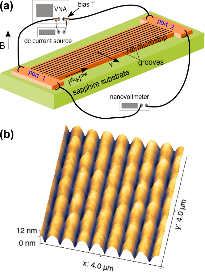
An array of 10 nm-deep, 50 nm-wide and 500 nm-spaced nanogrooves was milled by focused ion beam (FIB) in a high-resolution dual-beam microscope (FEI, Nova NanoLab 600). The grooves are parallel to the long side of the microstrip with a misalignment of less than 0.2∘, such that the vortices move across the grooves under the action of the transport current, Fig. 1. In the FIB milling process the beam parameters were 30 kV/50 pA, 1 s dwell time and 50 nm pitch. The microstrip width is an integer multiple number (300) of the nanopattern period to prevent possible ratchet effects due to the edge barrier asymmetry Pryadun et al. (2006). The background pinning in the epitaxial (110) Nb films is very weak as compared to the anisotropic pinning induced by the nanogrooves Dobrovolskiy et al. (2012).
The microwave vortex-state response was studied by cryogenic broadband spectroscopy Dobrovolskiy and Huth (2015) with magnetic field directed perpendicular to the film surface. The mw signal was generated and detected by an Agilent E5071C vector network analyzer (VNA). The mw and dc signals were superimposed and uncoupled by using two bias-tees mounted at the VNA ports. In what follows we only present the vortex-related contribution in the mw loss, as deduced from the relative change of the absolute value of the forward transmission coefficient where is the frequency- and mw-power-dependent reference loss at Lara et al. (2015); Cuadra-Solis et al. (2014).
III Results and discussion
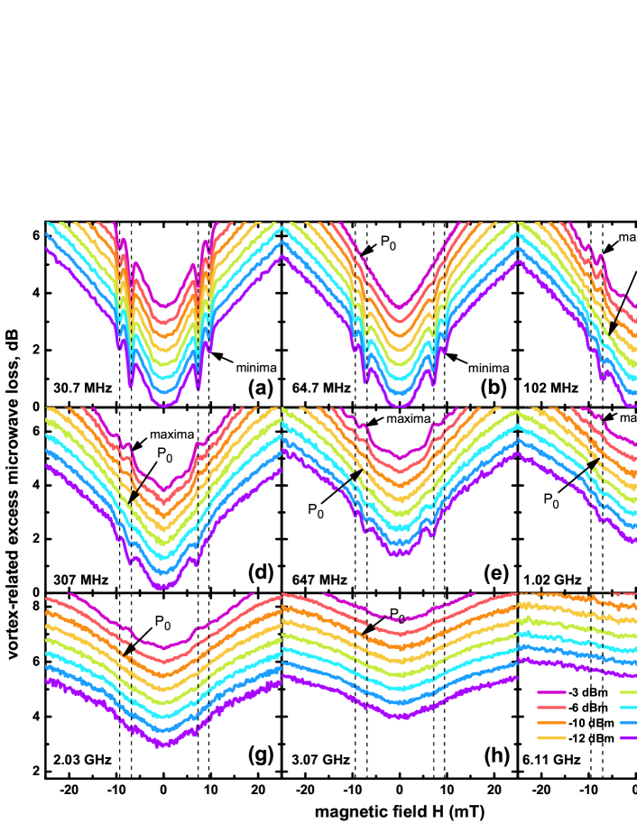
Figure 2 shows the vortex-related excess mw loss as a function of the magnetic field at for a series of ac frequencies. The mw loss is maximal at higher values as the number of vortices in the sample increases and it is minimal at , as expected. On the background of the smooth crossover from the minimal to the maximal mw loss value, one clearly recognizes spikes at the magnetic fields mT and mT in panels (a) to (g) of Fig. 2. The spike character evolves with increasing frequency and the spikes eventually vanish above GHz. At and the vortex lattice is commensurate with the 500 nm-periodic array of nanogrooves such that all vortices are pinned at the groove bottoms at 7.2 mT, which is referred to as a fundamental matching field. At mT one half of vortices is pinned at the groove bottoms while the rest are pinned between the grooves, so that this field value is referred to as a secondary matching field Dobrovolskiy and Huth (2015). The grooves are known to act as strong pinning sites for the vortex motion across them Dobrovolskiy et al. (2012); Serrano et al. (2016). Accordingly, the pinning of vortices is most efficient at , less so at and even less efficient at an arbitrary value of between and , say mT for definiteness. In the limit of low frequencies in Fig. 2(a), which corresponds to the quasistatic regime, one observes minima in the vortex-related mw excess loss at both matching fields for all mw power levels in the accessible range from -26 dBm to -3 dBm (2.5 W to 0.5 mW). Such matching dips are typically seen in the field dependence of the electrical dc resistance Serrano et al. (2016); Dobrovolskiy et al. (2012) or in the ac susceptibility in the linear regime at low mw power levels Cuadra-Solis et al. (2014); Dobrovolskiy and Huth (2015); Lara et al. (2015).
With increase of the frequency to 64.7 MHz in Fig. 2(b), at higher mw power levels, the minima become shallower and turn into maxima at MHz in Fig. 2(c). This crossover from minima to maxima at and is also seen in Fig. 2(d) to (g) with further increase of the frequency. It continues as long as the field dependence of the vortex-related mw excess loss does not become flattened at frequencies above the depinning frequency Gittleman and Rosenblum (1966); Coffey and Clem (1991); Shklovskij and Dobrovolskiy (2011) and the data become more noisy at yet higher frequencies. The depinning frequency has the physical meaning of the crossover frequency from the low-frequency regime, where the pinning forces dominate and the vortex response is weakly dissipative, to the high-frequency regime, where the frictional forces prevail and the response is strongly dissipative Pompeo and Silva (2008); Silva, Pompeo, and Dobrovolskiy (2017). The depinning frequency depends on the temperature Zaitsev et al. (2003), magnetic field Janjušević et al. (2006), and dc bias current Dobrovolskiy et al. (2017). The zero-temperature value for our sample is GHz, as deduced from fitting the data acquired at Dobrovolskiy et al. (2017) to the expression , yielding GHz at small fields and currents. This correlates reasonably well with the disappearance of the matching peculiarities in Fig. 2(g) as the pinning potential becomes less efficient for the vortex dynamics at higher frequencies. In all, the presence of the nanogroove array characterized by a strong washboard pinning potential allows for a direct comparison of the vortex-related mw loss for mobile and pinned vortices. However, this approach is limited to the frequency range below the depinning frequency, while the mw stimulation effect has been checked to continue up to the highest frequency accessible with our VNA (14 GHz), as inferred from the enhancement of and following the analysis of Ref. Lara et al. (2015). Importantly, no saturation of the stimulation effect at 14 GHz has yet been observed.
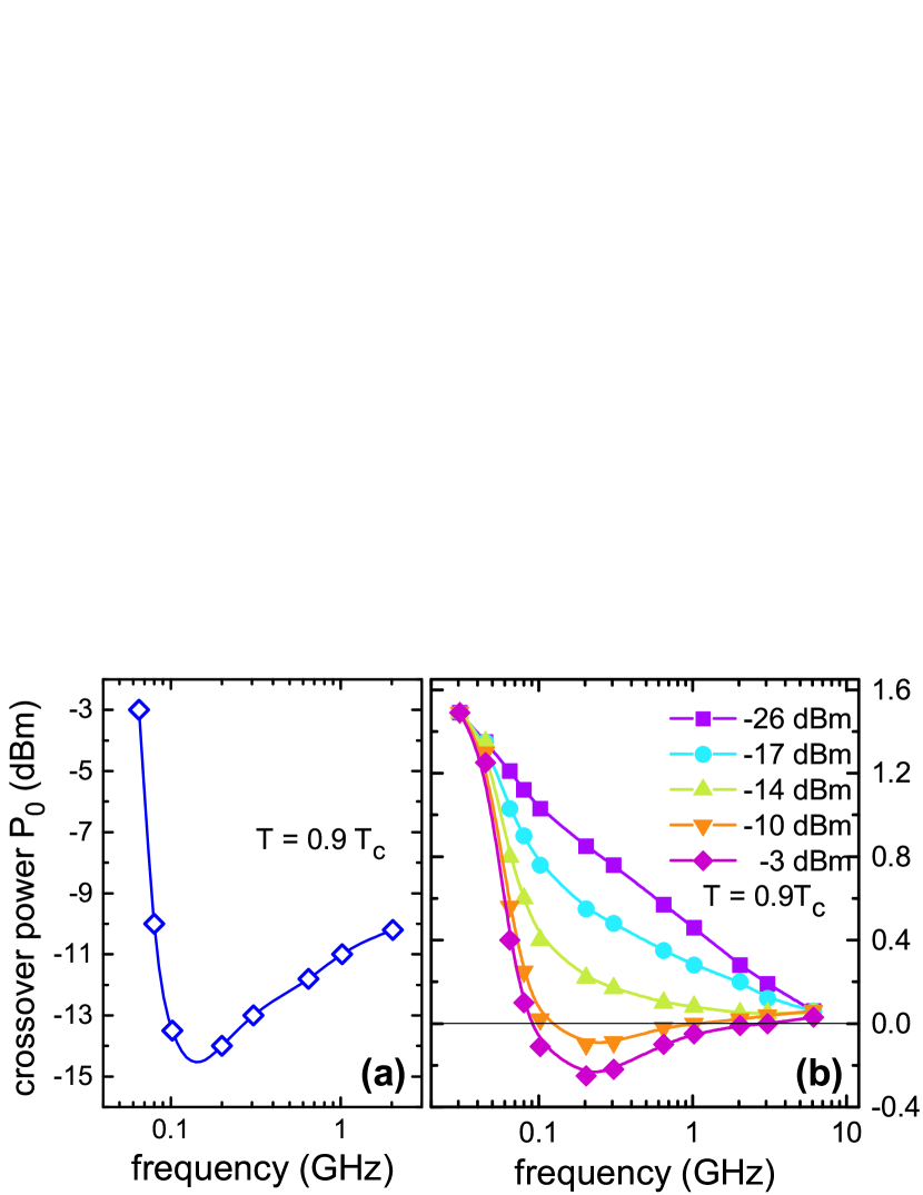
For a quantitative analysis of the excess mw loss due to mobile and pinned fluxons we introduce the crossover power corresponding to the crossover from the matching dips to peaks in Fig. 2. The evolution of as a function of the ac current frequency is shown in Fig. 3(a). At lower frequencies in the quasistatic regime there is no crossover from dips to peaks so that is undefined. The matching minima first vanish at MHz at a relatively high mw power of dBm. The stimulation effect becomes more efficient at higher frequencies such that decreases to about dBm and attains a minimum at about MHz. The further gradual increase of is associated with the approach of the depinning frequency , above which becomes undefined because of the vanishing difference in the contributions of pinned and mobile vortices.
The relative mw excess loss between the mobile and pinned fluxons is shown in Fig. 3(b). Positive loss values mean that pinned vortices dissipate less than the mobile ones while negative values result when the mobile vortices dissipate less than the pinned ones. The gradually decreasing loss difference at low mw power levels off with an increase of the frequency and reflects the delocalization transition in the vortex dynamics associated with the depinning frequency. Here, the relative loss is zero not exactly at but at about 8 GHz due to the smoothed functional shape of the crossover from the low-dissipative response at low frequencies to the strongly dissipative response at high frequencies Dobrovolskiy and Huth (2015). As is apparent from Fig. 3(b), there is no stimulation effect in the whole frequency range unless the mw power is larger than about dBm. Namely, as soon as the mw power exceeds the dBm level the stimulation effect occurs between and GHz and its magnitude becomes larger at dBm. This is accompanied by a broadening of the frequency range up to GHz where the mw loss due to mobile vortices is smaller than that due to the pinned ones.
While no upper frequency limit for the effect has been observed below 14 GHz, we have checked that the stimulation effect is suppressed as the mw power is further increasing to +6 dBm. This allows us to introduce an additional power parameter , at which a crossover from the stimulation to the suppression of superconductivity takes place. An extensive analysis of the stimulation effect on the thermodynamic (, ) and transport properties () will be published elsewhere. Here we just note that is related to the Joule heating and the stimulation of superconductivity between and is likely due to the effective cooling of the superconductor, which prevails over Joule heating caused by the current flow. Namely, under the action of the ac current of sufficiently high frequencies and power levels between and the quasiparticles leaving the vortex cores relax in an effectively larger superconducting volume due to the vortices shaken by the mw stimulus.
IV Conclusion
By comparing the vortex-related excess mw loss for mobile and pinned fluxons we have observed a crossover from mw loss minima at low frequencies to the regime of mw-stimulated vortex-state superconductivity above MHz in a certain range of mw power levels. The spatially periodic suppression of the superconducting gap in the vortex cores and the vortex dynamics under the action of the combination of dc and mw transport currents requires to simultaneously account for the kinetics of quasiparticles in conjunction with the spatial and temporal changes of the order parameter. While a theoretical description of the observed effect is yet to be elaborated we attribute our findings to a competition of the effective cooling of the system by quasiparticles leaving the vortex cores with the conventional Joule heating associated with the current flow.
Acknowledgements
OD thanks the German Research Foundation (DFG) for support through Grant No 374052683 (DO1511/3-1). AL and FA acknowledge support by Spanish MINECO (MAT2015-66000-P) and Comunidad de Madrid (NANOFRONTMAG-CM S2013/MIT-2850) Grants. This work was supported by the European Cooperation in Science and Technology by via COST Action CA16218 (NANOCOHYBRI). Further, funding from the European Commission in the framework of the program Marie Sklodowska-Curie Actions — Research and Innovation Staff Exchange (MSCA-RISE) under Grant Agreement No. 644348 (MagIC) is acknowledged.
References
- Wyatt et al. (1966) A. F. G. Wyatt, V. M. Dmitriev, W. S. Moore, and F. W. Sheard, Phys. Rev. Lett. 16, 1166 (1966).
- Pals and Dobben (1979) J. A. Pals and J. Dobben, Phys. Rev. B 20, 935 (1979).
- Tolpygo and Tulin (1983) S. K. Tolpygo and V. A. Tulin, Sov. Phys. JETP 57, 123 (1983).
- Heslinga and Klapwijk (1993) D. R. Heslinga and T. M. Klapwijk, Phys. Rev. B 47, 5157 (1993).
- Pals and Dobben (1980) J. A. Pals and J. Dobben, Phys. Rev. Lett. 44, 1143 (1980).
- Entin-Wohlman (1981) O. Entin-Wohlman, Phys. Rev. B 23, 2428 (1981).
- Beck et al. (2013) M. Beck, I. Rousseau, M. Klammer, P. Leiderer, M. Mittendorff, S. Winnerl, M. Helm, G. N. Gol’tsman, and J. Demsar, Phys. Rev. Lett. 110, 267003 (2013).
- de Visser et al. (2014) P. J. de Visser, D. J. Goldie, P. Diener, S. Withington, J. J. A. Baselmans, and T. M. Klapwijk, Phys. Rev. Lett. 112, 047004 (2014).
- Eliashberg (1970) G. M. Eliashberg, JETP Lett. 11, 186 (1970).
- Aslamazov and Larkin (1978) L. G. Aslamazov and A. I. Larkin, Zh. Eksp. Teor. Fiz. 74, 2184 (1978).
- Aslamazov and Lempitskii (1982) L. G. Aslamazov and S. V. Lempitskii, Zh. Eksp. Teor. Fiz. 82, 1671 (1982).
- Lempitskil (1983) S. V. Lempitskil, Zh. Eksp. Teor. Fiz. 85, 1072 (1983).
- Zolochevskii (2013) I. V. Zolochevskii, Low Temp. Phys. 39, 571 (2013).
- Dobrovolskiy, Huth, and Shklovskij (2015) O. V. Dobrovolskiy, M. Huth, and V. A. Shklovskij, Appl. Phys. Lett. 107, 162603 (2015).
- Kompaniiets et al. (2014) M. Kompaniiets, O. V. Dobrovolskiy, C. Neetzel, F. Porrati, J. Brötz, W. Ensinger, and M. Huth, Appl. Phys. Lett. 104, 052603 (2014).
- Winhold et al. (2014) M. Winhold, P. M. Weirich, C. H. Schwalb, and M. Huth, Appl. Phys. Lett. 105, 162603 (2014).
- Sengupta et al. (2015) S. Sengupta, C. Li, C. Baumier, A. Kasumov, S. Guron, H. Bouchiat, and F. Fortuna, Appl. Phys. Lett. 106, 042601 (2015), .
- Tsindlekht et al. (2016) M. I. Tsindlekht, V. M. Genkin, I. Felner, F. Zeides, N. Katz, E. Gazi, E. Chromik, O. V. Dobrovolskiy, R. Sachser, and M. Huth, J. Phys.: Condens. Matter 28, 215701 (2016).
- Fomin, Rezaev, and Schmidt (2012) V. M. Fomin, R. O. Rezaev, and O. G. Schmidt, Nano Lett. 12, 1282 (2012), .
- Rezaev, Fomin, and Schmidt (2014) R. O. Rezaev, V. M. Fomin, and O. G. Schmidt, Physica C 497, 1 (2014).
- Cordoba et al. (2018) R. Cordoba, A. Ibarra, D. Mailly, and J. M. De Teresa, Nano Lett. 18, 1379 (2018), NoStop
- Thurmer et al. (2010) D. J. Thurmer, C. C. B. Bufon, C. Deneke, and O. G. Schmidt, Nano Lett. 10, 3704 (2010).
- Serrano et al. (2016) I. G. Serrano, J. Sese, I. Guillamon, H. Suderow, S. Vieira, M. R. Ibarra, and J. M. De Teresa, Beilstein J. Nanotechnol. 7, 1698 (2016).
- Huth, Porrati, and Dobrovolskiy (2018) M. Huth, F. Porrati, and O. V. Dobrovolskiy, Microelectr. Engin. 185-186, 9 (2018).
- Makise et al. (2014) K. Makise, K. Mitsuishi, M. Shimojo, and B. Shinozaki, Sci. Rep. 4, 5740 (2014).
- Marsili et al. (2013) F. Marsili, V. B. Verma, J. A. Stern, S. Harrington, A. E. Lita, T. Gerrits, I. Vayshenker, B. Baek, M. D. Shaw, R. P. Mirin, and S. W. Nam, Nat. Photon. 7, 210 (2013).
- Lehtinen et al. (2017) J. S. Lehtinen, E. Mykkänen, A. Kemppinen, S. V. Lotkhov, D. Golubev, and A. J. Manninen, Supercond. Sci. Technol. 30, 055006 (2017).
- Dobrovolskiy and Huth (2015) O. V. Dobrovolskiy and M. Huth, Appl. Phys. Lett. 106, 142601 (2015).
- Vlasko-Vlasov et al. (2016) V. K. Vlasko-Vlasov, F. Colauto, T. Benseman, D. Rosenmann, and W.-K. Kwok, Sci. Rep. 6, 36847 (2016).
- Dobrovolskiy et al. (2018) O. V. Dobrovolskiy, R. Sachser, M. Huth, V. A. Shklovskij, R. V. Vovk, V. M. Bevz, and M. I. Tsindlekht, Appl. Phys. Lett. 112, 152601 (2018), .
- Wallraff et al. (2004) A. Wallraff, D. I. Schuster, A. Blais, L. Frunzio, R.-S. Huang, J. Majer, S. Kumar, S. M. Girvin, and R. J. Schoelkopf, Nature 431, 162 (2004).
- Hofheinz et al. (2009) M. Hofheinz, H. Wang, M. Ansmann, R. Bialczak, E. Lucero, M. Neeley, A. D. O’Connell, D. Sank, J. Wenner, J. M. Martinis, and A. N. Cleland, Nature 459, 546 (2009).
- DiCarlo et al. (2009) L. DiCarlo, J. M. Chow, J. M. Gambetta, L. S. Bishop, B. R. Johnson, D. I. Schuster, J. Majer, L. Blais, A. Frunzio, S. M. Girvin, and R. J. Schoelkopf, Nature 460, 240 (2009).
- Lara et al. (2015) A. Lara, F. G. Aliev, A. V. Silhanek, and V. V. Moshchalkov, Sci. Rep. 5, 9187 (2015).
- Dobrovolskiy (2017) O. V. Dobrovolskiy, Physica C 533, 80 (2017).
- Dobrovolskiy and Huth (2012) O. V. Dobrovolskiy and M. Huth, Thin Solid Films 520, 5985 (2012).
- Pryadun et al. (2006) V. V. Pryadun, J. Sierra, F. G. Aliev, D. S. Golubovic, and V. V. Moshchalkov, Appl. Phys. Lett. 88, 062517 (2006).
- Dobrovolskiy et al. (2012) O. V. Dobrovolskiy, E. Begun, M. Huth, and V. A. Shklovskij, New J. Phys. 14, 113027 (2012).
- Cuadra-Solis et al. (2014) P.-d.-J. Cuadra-Solis, A. Garcia-Santiago, J. M. Hernandez, J. Tejada, J. Vanacken, and V. V. Moshchalkov, Phys. Rev. B 89, 054517 (2014).
- Gittleman and Rosenblum (1966) J. I. Gittleman and B. Rosenblum, Phys. Rev. Lett. 16, 734 (1966).
- Coffey and Clem (1991) M. W. Coffey and J. R. Clem, Phys. Rev. Lett. 67, 386 (1991).
- Shklovskij and Dobrovolskiy (2011) V. A. Shklovskij and O. V. Dobrovolskiy, Phys. Rev. B 84, 054515 (2011).
- Pompeo and Silva (2008) N. Pompeo and E. Silva, Phys. Rev. B 78, 094503 (2008).
- Silva, Pompeo, and Dobrovolskiy (2017) E. Silva, N. Pompeo, and O. V. Dobrovolskiy, Phys. Sci. Rep. 10, 20178004 (2017).
- Zaitsev et al. (2003) A. G. Zaitsev, R. Schneider, G. Linker, F. Ratzel, R. Smithey, and J. Geerk, Phys. Rev. B 68, 104502 (2003).
- Janjušević et al. (2006) D. Janjušević, M. S. Grbić, M. Požek, A. Dulčić, D. Paar, B. Nebendahl, and T. Wagner, Phys. Rev. B 74, 104501 (2006).
- Dobrovolskiy et al. (2017) O. V. Dobrovolskiy, M. Huth, V. Shklovskij, and R. V. Vovk, Sci. Rep. 7, 13740 (2017).