Large-scale tight-binding simulations of quantum transport in ballistic graphene
Abstract
Graphene has proven to host outstanding mesoscopic effects involving massless Dirac quasiparticles travelling ballistically resulting in the current flow exhibiting light-like behaviour. A new branch of 2D electronics inspired by the standard principles of optics is rapidly evolving, calling for a deeper understanding of transport in large-scale devices at a quantum level. Here we perform large-scale quantum transport calculations based on a tight-binding model of graphene and the non-equilibrium Green’s function method and include the effects of junctions of different shape, magnetic field, and absorptive regions acting as drains for current. We stress the importance of choosing absorbing boundary conditions in the calculations to correctly capture how current flows in the limit of infinite devices. As a specific application we present a fully quantum-mechanical framework for the “2D Dirac fermion microscope” recently proposed by Bøggild et al. [Nat. Comm. 8, 10.1038 (2017)], tackling several key electron-optical effects therein predicted via semiclassical trajectory simulations, such as electron beam collimation, deflection and scattering off Veselago dots. Our results confirm that a semiclassical approach to a large extend is sufficient to capture the main transport features in the mesoscopic limit and the optical regime, but also that a richer electron-optical landscape is to be expected when coherence or other purely quantum effects are accounted for in the simulations.
I Introduction
Graphene has proven to be the scene of unprecedented mesoscopic effects, hosting massless Dirac quasiparticles that travel with little scattering. These relativistic charge carriers can move ballistically across m-long distances at room temperature Taychatanapat2013 , so far reaching mean free paths of the order 30 m at low temperatures Banszerus2016 . They can undergo negative refraction when passing junctions Cheianov2007 and can be manipulated by external electromagnetic fields Chen2016 , thus being easily emitted, collimated, steered or focused like rays of light. As a result a new type of 2D electronics complying with the principles of optics is rapidly finding its way in the 2D materials community, supported by the relentless progress towards large-scale production of high-quality graphene.
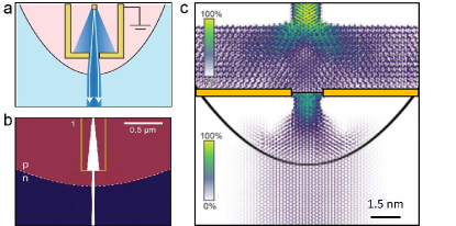
One example, recently brough up by Bøggild and co-authors Boggild2017 , is to combine different graphene-based electron-optics components in a “2D Dirac fermion microscope” (DFM) as in Fig. 1. Here electron emitters/guns, collimating apertures Barnard2017 , tunable lenses, deflectors, and detectors are imagined to be incorporated in a graphene “vacuum chamber” to image different types of targets, such as metal-graphene interfaces, grain boundaries, edges, defects, adsorbed molecules, nanoparticles, quantum dots, or plasmonic superstructures. The authors provide a perspective view on how such a tool can be realistically implemented and operated, proposing practical architectures and design rules for all of its 2D components, based on state-of-the-art achievements in graphene technology.
The approach used by Bøggild et al. for large-scale electron transport simulations is purely semiclassical and belongs to a broadly used class of simulation known as billiard models. In the last few years these models have proven to successfully provide insights on the overall magneto-transport characteristics of graphene Miao2007 ; Lackner2013 ; Taychatanapat2015 ; Wurm2011 and other large-scale ballistic devices in the mesoscopic limit Molenkamp1990 .
However, despite allowing computation with little time and memory consumption, semiclassical transport simulations always need to be calibrated with measured macroscopic parameters, such as mobility or diffusion coefficients. Most importantly, quantum effects such as coherence are not naturally included in semiclassical simulations, despite their importance for describing phenomena such as magnetic focusing, chiral tunneling in the ballistic regime or conductance fluctuations in the diffusive regime Caridad2016 ; Jiang2017 . Diffraction is also expected to have major implications in devices where Dirac fermions pass through apertures smaller than their Fermi wavelength or scatter off small objects. Future realization and operation of complex relativistic electron-optics graphene systems thus calls for a deeper understanding of transport at the quantum level, where the full quantum nature of Dirac fermions is accounted for.
Along this line it is also decisive to be able to access simulations at the scale of experimental devices, which often range from hundreds of nano-meters to a few microns. At the same time it is crucial to provide reliable benchmarks to measurements in the presence of defects, interfaces, or disorder, where details matter on the atomic scale. The huge number of atoms contained in the typical experimental systems prohibits the application of usual ab-initio electronic structure techniques like density functional theory (DFT), where the detailed quantum-chemical structure of every atom is taken into account. Hence, the development of novel high-performance computational methods to enable quantum transport simulations at experimentally relevant device dimensions is essential.
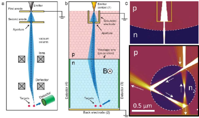
Here we perform quantum transport calculations of large tight-binding (TB) models of graphene using the non-equilibrium Green’s function method (NEGF). We will report on the multi-functionality and performance of our tools while studying transport in large graphene flakes on the scale of hundreds of in the presence of junctions, magnetic field and/or absorptive regions. Our main focus will be to reproduce from a fully atomistic perspective some key features of electron transport in a DFM, such as electron beam collimation, deflection, and scattering off circular Veselago dots (VD) Cheianov2007 . We will emphasize how different choices of boundary conditions lead to different density patterns, providing a simple computational solution to minimize the occurrence of artificial features in the current, e.g. using hard-wall or periodic boundaries. The manuscript is organized as follows. We will first briefly review the state of the art of the computational methods that can be used for transport simulations of large-scale graphene devices. This is followed by an overview of the used methods, the code, and the setup we use to carry out our calculations. We will then discuss the effects of adopting different boundary conditions in the device. To conclude we will present a direct comparison between our results and those reported in Boggild2017 , highlighting similarities and differences between the semiclassical and quantum simulations.
I.1 Methods for large-scale graphene transport simulations
For any quantum transport technique to efficiently address realistic graphene devices, it is vital to describe the underlying electronic structure in a computationally efficient manner. A broadly adopted solution is to model the electronic structure of graphene using the tight-binding approximation CastroNeto2009 ; FoaTorres ; Meunier2016 . This approximation is in its “cheapest” textbook version, where the Hamiltonian is orthogonal and includes only interactions between nearest-neighbor () orbitals, able to capture the main qualitative features of the graphene band structure. Due to its versatility, this method has often been at the center of new improvements and developments. In particular we point out the simple scaling approach proposed by Liu et al. Liu2012 ; Liu2015 , who provide a simple condition to obtain band structure invariance, while simultaneously adjusting the lattice constant and the hopping parameter in tight-binding models of graphene. A similar approach is the one suggested by Beconcini et al. Beconcini2016 , who manage to achieve band structure invariance by using the Fermi energy as key scaling parameter, thus accessing simulations of multi-terminal devices and nonlocal transport measurements. In more detail, they show that a geometrical downward scaling of the system size can be accompanied by an upward scaling of the Fermi energy in such a way that the number of electronic states responsible for transport is kept constant. Both of these scaling approaches have proven to be very efficient tools to interpret magnetic focusing experiments involving micron-size multi-terminal devices Petrovic2017 ; Lagasse2017 , where factors such as edges, chemical functionalization, structural disorder or contact with metal do not disrupt the relevant transport features.
Electron transport for very large system dimensions can then be achieved by coupling a TB Hamiltonian with different quantum transport formalisms Uppstu2014 . For example, hybrid Monte Carlo algorithms on lattice Buividovich2012 or Wave-Packet Dynamics Mark2017 ; Vancso2014 ; Krueckl2009 ; Haefner2011 have been used to study large-scale transport in graphene. The latter in particular is a very intuitive method which has the advantage of giving direct access to the real-space and real-time electron wave-packet propagation over a graphene lattice. Here energy resolution can be obtained by Fourier transforming in time domain, at the cost of including a very fine time discretization. The majority of the other transport formalisms are based on the Landauer-Büttiker theory. The Kubo-Greenwood formalism is a very popular example Ortmann2011 ; Lherbier2012 ; BarriosVargas2017 ; Calderin2017 ; Ervasti2015 , which turns out to be an ideal choice when studying diffusive large-scale graphene systems described by a mobility or conductivity. Along similar lines the patched Green’s function technique can be used to introduce open-boundary self-energy terms in the device Hamiltonian to describe its connection to an infinite sample Settnes2015 . Complementary to this the TB-NEGF method is a popular choice for ballistic transport Datta2000 where the target is most often conductance including explicit descriptions of multiple electrodes, rather than conductivity. It allows for self-consistent mean-field description of the potential, e.g. using a Hubbard-type modelHancock2010 including the possibility to study the effect of spin-polarization. Many simulation packages are now implementing the NEGF scheme as a standard feature to calculate electron transport in nanostructures, enabling its application to tight-binding Hamiltonians as well as other electronic structure models with higher level of accuracy such as DFT Brandbyge2002 which can scale linearly with length of the system in the transport direction using recursive Green’s function methods.
II Computational tools
Our quantum transport simulations are based on the NEGF method and a nearest-neighbour TB Hamiltonian using the standard expressions of transmission in terms of the retarded Green’s function Datta1997; Datta2000 . For the particular implementation we use the open-source TBtrans and sisl Papior2017 ; Papior2017a tools distributed with the TranSiesta software package Papior2017 . TranSiesta is a tool for high-performance DFT+NEGF self-consistent calculations. It relies on advanced matrix inversion algorithms to efficiently obtain the Green’s functions for large, multi-terminal systems at various electrostatic conditions (e.g. gating Papior2015 ), while the charge-density is obtained using contour integration of the spectral densities.
TBtrans is a “post-processing” NEGF code which provides a flexible interface to DFT as well as user-defined tight-binding Hamiltonians, using Python as back-end. It enables large-scale tight-binding transport calculations of spectral physical quantities, interpolated - curves, transmission eigenchannels Papior2017 and/or orbital/bond-currents for setups that can easily exceed millions of orbitals on few-core machines. The possibility of using Bloch expansion for electrodes with periodicity transverse to the transport direction and customizing the effective shape of the device region makes it possible to increase the scale of transmission calculations even furtherPapiorThesis . Complementary to TBtrans sisl was developed as a Python package to create and manipulate large-scale (non-)orthogonal tight-binding models for arbitrary geometries, with any number of orbitals and any periodicity. It allows to read external Hamiltonians and real-space grids from various DFT programs (e.g. Siesta Soler2002 or Wannier90 Mostofi2014 ), providing user-friendly routines for post-processing and output of electronic structure and transport calculations. To include the effects of doping, magnetic field or absorptive potentials in our system we exploit the TBtrans capability of customizing the device Green’s function via real (complex) - (energy-) dependent perturbative terms:
| (1) |
Here and are the unperturbed overlap and Hamiltonian in the device region, while is the self-energy for each semi-infinite electrode . If we call , and the - and energy independent perturbations to the Hamiltonian caused by junctions, absorptive regions (like those simulated using complex absorbing potential (CAP) Xie2014 ; Yu2015 ) and magnetic field , respectively, we can incorporate the effects of these mechanisms in the expression for as:
| (2) |
In the following sections we provide details on the physics behind the terms in Eq. (2) and how we construct them in the TB calculation.
We use sisl to set up a nearest-neighbor orthogonal TB Hamiltonian for a two-probe graphene device, with carbon-carbon bond length and hopping parameter . Our supercell, inspired by the hetero-dimensional graphene junctions studied in Wang2010 , consists of a wide zigzag graphene nanoribbon acting as point-like source electrode at the edge of a graphene flake with atoms (sites).
II.1 p-n junctions
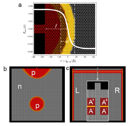
In an orthogonal tight-binding model doping is straightforward to introduce via a global or local adjustment of the diagonal (on-site) elements of the Hamiltonian. In our calculations we generate smooth symmetric junctions using:
| (3) |
where the junction potential profile is given by
| (4) |
and the junction thickness is set to . The junction profile can be chosen to be linear or can conveniently be shaped to achieve Veselago lensing of electrons Chen2016 . In particular, as suggested by Liu et al. Liu2017 , electrons can be focused into a sharp collimated beam using a parabolic junction with focal point located at the point source. In our model for the DFM source we thus make use of such shape, placing the parabola at a focal distance from the injection point, as illustrated in Fig. 2a and b. In the same figure we show that this method also can be used to construct circular p-n juctions, or Veselago dots (VD) Cserti2007 , here used as targets for the collimated beam of electrons.
II.2 Complex absorbing potential (CAP)
In standard NEGF transport problems one usually deals with infinite open systems, where semi-infinite leads are included in the calculation of the Green’s function via a self-energy in the device Hamiltonian. For large geometries a major computational limitation is the number and the size of semi-infinite leads. This limitation can be efficiently overcome by replacing the Hamiltonian of the leads with complex absorbing potentials (CAP) that completely absorb the incident wave-function Xie2014 ; Yu2015 . This method allows reduction of the original open system to a finite closed system without disrupting current conservation. For example, the Hamiltonian matrix for a two-probe system where CAP is used to replace the electrode self-energies can be written as the sum of the standard two-probe Hamiltonian matrix plus a purely imaginary term added to the diagonal matrix elements:
| (5) |
Here we assume transport to occur along the direction, and define and as
| (6) |
where is a smooth function of the form
| (7) |
Here and are the starting and ending points of the CAP region in the device, respectively, is its length and is a constant numerical parameter set to be equal to 2.62 Yu2015 . Note how diverges as tends to , turning the semi-infinite lead into a finite lead. The CAP expression in Eq. (6) is based on purely semiclassical arguments, and may lead to reflection at , which reduces the final transmission. However this can be mitigated by increasing the length of the CAP region, until the spectra are in agreement with those obtained in the original open system. In order to estimate a suitable value for the thickness of CAP regions in our device configuration, we have calculated transmission using semi-infinite source and drain electrodes along and applying periodic boundary conditions (PBC) along the transverse direction . We then compared this with the transmission obtained by setting CAP rather than PBC on the cell boundaries along . We find that an almost exact overlap between the two spectra is achieved by setting .
CAP can also be used to design narrow absorbing areas such as those generated by contacts with grounded electrodes Barnard2017 . A proper comparison with simulations of a DFM reported in Ref. Boggild2017 requires an isotropic point-like source of electrons. However, a hetero-dimensional graphene junction, such as the ribbon considered here, is known to produce isotropic injection only for electron energies very close to the Dirac point, whereas preferential injection takes over at higher energies, with angles depending on the ribbon symmetry Wang2010 . In order to ensure isotropic injection we therefore place an absorptive pinhole with an opening of at a distance of from the ribbon/flake interface, mimicking apertures generated by grounded electrodes Barnard2017 . In Fig. 2c we highlight in red the areas of our model where a CAP is used, indicating with a yellow line the points where diverges from both sides. Notice how CAP is set separately on front- and back-side of the pinhole, labeled A+ and A-, respectively.
II.3 Magnetic field
A transverse magnetic field in a graphene device can be included in the off-diagonal elements of the Hamiltonian via Peierls substitution Luttinger1951 ; Pedersen2011 . We can formally write this as an additive term to the unperturbed Hamiltonian,
| (8) |
where the phase factor is multiplied on each matrix element of , in a coordinate system where the axis is aligned with graphene armchair direction. The phase can be written as
| (9) |
with being the quantum magnetic flux.
We implement this approach in sisl/TBtrans and as a benchmark we have compared to the popular quantum transport code kwantGroth2014 , finding good agreement.
II.4 Visualization of bond-currents
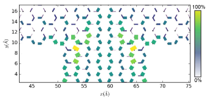
Bond currents allow imaging of spatial profiles of nonequilibrium charge and current densities in solid-stateDatta2000 ; Nonoyama1998 as well as molecular-scale systemsSolomon2010 . They represent local current flowing in the inter-atomic bonds and are defined as the sum over all orbital (indices ) currents, . After being generalized for use in honeycomb lattices Zarbo2007 direct insights could be provided into how the massless Dirac fermions propagate between two neighboring lattice sites in graphene and other carbon nanostructures. There is still no well established way of visualizing bond-currents. In general they can be visualized as flow lines mapped on the network of lattice bonds. Arrow vectors are typically used, whose thickness or length is proportional to the magnitude of the current flowing between each pair of neighbouring atoms Mason2013 ; GomesdaRocha2015 ; Stuyver2017 ; Nozaki2017 . This approach provides useful information about both magnitude and direction of the current flowing through the system. However if large geometries are considered it is not feasible due to the overwhelming number of connections to be visualized. A solution to this is to visualize bond-currents on a coarse grained grid, where only a proper average of bond-currents within each cluster is shown as a single arrow Settnes2015 . In this case the final result will of course depend on the cluster size and on the way the average is carried out, but nevertheless it allows to scale the dimensions of the image at wish enabling access to useful current maps for very large system dimensions.
Here we visualize bond-currents as line segments of length aligned along a line connecting each pair of neighbour sites, as illustrated in Fig. 3. We select only positive bond currents and for each of them we draw a segment having one extremity at the lattice site from which the relative current originates. We scale the segment thickness and color in proportion to the current magnitude, so that areas with low to zero current will appear white because the bond width is reduced to zero. This approach allows us to access graphene geometries with arbitrary large size, retaining full information about current directionality without a need for user-defined post-processing of the data. The same color map is adopted and color and thickness are always normalized to the maximum value of bond-current in the system. Sometimes the color range is adjusted in order to enhance contrast. If not stated otherwise, bond currents are always computed at .
II.4.1 Performance of TBtrans and sisl
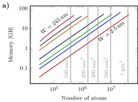
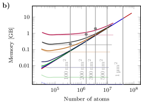
The calculations are performed using TBtrans which implements a highly advanced block-tri-diagonal inversion algorithm which minimises calculationsPapior2017 . The main difficulty in calculating very large systems is the calculation of bond-currents and orbital-resolved DOS, which requires the spectral function () for a given electrode . In Fig. 4 we show the memory requirements of TBtrans for the very large nearest-neighbour graphene devices with periodic boundary conditions. In both a) and b) vertical lines indicate system sizes of square unit cells of noted area. Lines are ascending together with cell width, the narrowest cell being and the widest (see a). In Fig. 4a the total memory requirements is plotted when calculating physical quantities for the full system in one calculation. This is scaling linearly with respect to system size. Since TBtrans has been implemented with 4-byte integers, there is an upper limit to the size of the allocated block tri-diagonal matrix. I.e. the lines stop due to integer overflow in the code. Fig. 4b shows memory requirements when only calculating quantities for a selected region in the device, here chosen to include 4 lines of carbon atoms. Clearly the memory requirements drastically reduces and becomes feasible on laptop computers. Here the gray dots indicate the memory requirements for the square unit cells of given area. The transparent lines represent the memory usage of the block tri-diagonal matrices, which become constant for large systems. Thus, the only memory increase is due to the sparse matrices used to retain the Hamiltonian and bond currents etc.
TBtrans is parallelized using both MPI and OpenMP enabling high-performance calculations with large throughput. In these calculations (400.000 nearest neighbour atoms) we use 24 OpenMP threads and runs in roughly 1 minute per energy point using XeonE5-2650 machines.
A full setup, transmission calculation and post-processing using sisl and TBtrans takes approximately 40 minutes, with a similar amount of time spent on setting up input and plotting.
We have shown how large scale calculations can efficiently be calculated and post-processed. Further information about sisl may be found in Ref. Papior2017a .
III Results
We use the methods presented in the previous sections to create a tight-binding model of a DFM. In Fig. 5 we illustrate the definitive model that we use to generate collimated beams of electrons in our calculations. Electrons are injected by a ribbon, filtered by an absorptive pinhole and further collimated by a parabolic junction. As reported in Wang2010 , injection at the interface between the ribbon and the large flake is largely anisotropic and can be made isotropic by using a CAP region as an absorptive pinhole. The result is in good agreement with both the semiclassical calculations reported in Boggild2017 and the tight-binding calculations by Liu et al. Liu2017 .
III.1 Boundary conditions
Choosing the correct boundary conditions is essential in reproducing the wanted physical pictures. The goal of the DFM example discussed below is the analysis of collimated beams injected into large graphene samples. Here we emphasize the importance of selecting appropriate boundary conditions to simulate such device in its limit of infinite extension. Fig. 2c is used in the following where we call L (R) the left (right) boundary of the large flake, A+ the CAP region that acts as pin-hole injector and A- the pinhole side that faces opposite to the source. On the opposite side of injection a regular lead is placed. In Fig. 6 we analyze bond-currents in the area beyond the parabolic lens at different applied magnetic fields and various boundary conditions, progressively switching on the CAP regions at L, R and A-. In the following CAP at A+ is always used to ensure a collimated pin-hole injector.
The most straight-forward approach here would be to use periodic boundary conditions at L and R, as considered in Fig. 6a. In general this represents a very popular choice for electronic structure calculations, where even the presence of local perturbations in the system, e.g. defects or adsorbed molecules, can be accurately dealt with by increasing the cell size and thus minimizing the periodic interactions. However it is known that often periodicity is not able to correctly describe the relevant features in non-equilibrium transport calculations Lagasse2017 . As shown in Fig. 6a, despite the very large cell used (), interaction between periodic repetitions of the source give rise to significant interference in the currents pattern. At the collimated beam is still visible behind the interference fringes, while it gets progressively suppressed as the magnetic field increases. The situation is somewhat similar when periodicity in L and R is replaced with hard-wall high potentials acting as barriers (Fig. 6b), except that in this case much more interference occurs at high B fields. An effective solution to this problem is to use CAP at L and R, similar to what Lagasse and coauthors suggest in Ref. Lagasse2017 . In Fig. 6c the interference is indeed reduced, especially at higher B fields, where the beam is now clearly visible beyond the fringes. Nevertheless one can notice that the electron beam is still not very well collimated: already at it splits into several narrow beams after crossing the parabolic lens. This is due to internal reflections occurring between the parabolic junction and the region A- of the pinhole, which in Fig. 6c is not equipped with CAP. This is an artificial effect, since realistic grounded electrodes contacting graphene to create apertures would at least partly Barnard2017 absorb electrons impinging onto them from all possible directions. In Fig. 6d we demonstrate that this backscattering effect can be eliminated by switching on CAP at the A- region. The combined application of CAP in L, R, A- eventually allows us to get rid of most interference effects for all magnetic fields considered, see Fig. 6e.
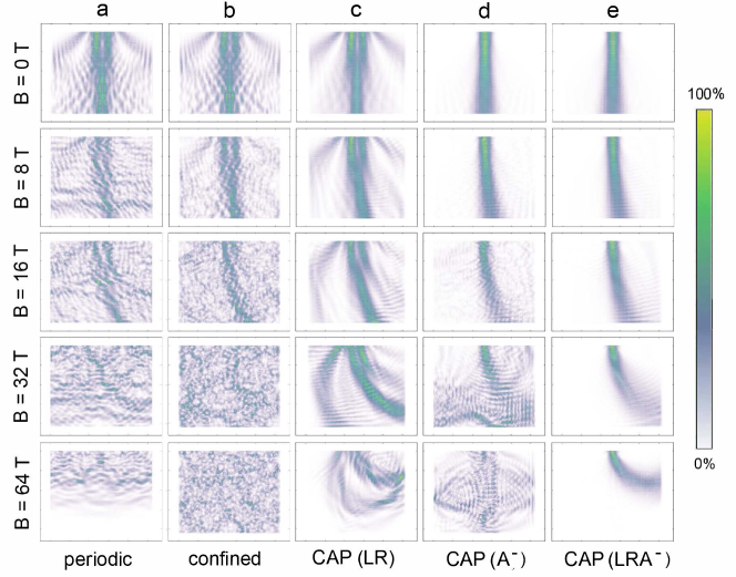
We conclude that investigating an injected beam in the limit of infinite graphene devices requires a specific and an elaborate set of boundary conditions to filter out artificial backscattering processes. Importantly a A--side CAP is necessary to absorb backscattered electrons from the junction as well as beam-bending from the magnetic field.
III.2 Comparison with semiclassical simulations of DFM
In order to gain a deeper insight on the role of quantum coherence effects in the DFM, we consider some of the systems studied in Ref. Boggild2017 where collimated electron beams are focused onto circular Veselago dots (VD) of various size. We concentrate on the mesoscopic limit, , where the mean free path of electrons is larger than the characteristic length of the system, which in turn is much larger compared to the Fermi wavelength . In the following we consider explicitly the situation that the phase coherence length is infinite, i.e. that the system is fully coherent.
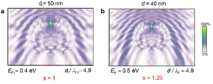
We note that the area available for the quantum simulations is smaller than the structures considered in realistic setups such as those in Ref. Boggild2017 . We deal with this by effectively scaling the graphene bond-length while retaining the number of atoms in our TB model via a scaling parameter , defined as the ratio between the real diameter of the full, non-scaled VD that we would like to simulate and the actual diameter of the VD designed in our geometry. We assume to be the electron density in the non-scaled pristine graphene system, which (in the linear band approximation) corresponds to and . A qualitatively correct electron flow around the VD of diameter in our bond-currents calculations can thus be captured by simply dividing the Fermi wavelength by the scaling factor , yielding and . The key step of the scaling procedure is to keep the diameter vs. Fermi-wavelength ratio constant Heinisch2013 ; Caridad2016 ; Jiang2017 . This approach can be thought as a particular case of the more general scaling method presented in Beconcini2016 , hence we refer readers to this for further details.
Our scaling method is exemplified in Fig. 7. Let us assume that the VD on the left with is the original non-scaled VD that we want to study (). In Fig. 7b we demonstrate that by applying the scaling procedure with we are able to reduce the VD size and produce bond-currents inside and outside the VD which are indistinguishable from Fig. 7a. In general, this approach enables us to effectively simulate systems that are times larger than the actual geometry considered in our calculations. Using , for example, is equivalent to analyze a graphene system with an equivalent number of atoms.
In the following we will always indicate above every figure the full, non-scaled diameter of the VD, while below we will provide the diameter vs. Fermi-wavelength ratio considered and the value of used to scale the system down to our -orbitals TB model.
Figure 8 shows caustic patterns inside VD with different scaled diameters, namely , and , generated by scattering of a wide beam of electrons collimated with a parabolic lens in front of a aperture. These diameters correspond to scaling parameters , and , respectively, allowing us to compare to some of the systems studied by semi-classical simulations in Ref. Boggild2017 . We focus on the area inside the dot and observe characteristic caustic patterns at all energies which are in reasonable agreement with the results reported in Ref. Boggild2017 and by Agrawal et al. AgrawalGarg2014 . This is especially true with regard to the position of the main cusp in the first caustic line.
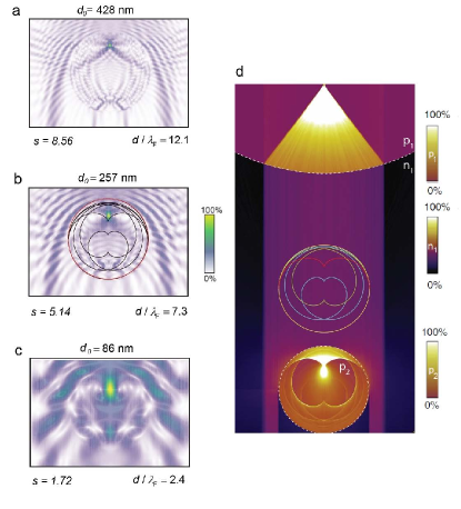
A better description of the higher order caustics while keeping Fermi energies () within the limits of the linear band approximation would require creation of VD with scaled diameters at least 2–3 times larger than the ones considered here, i.e. , which is not possible within our graphene flake. For similar dot dimensions quantum mechanical calculations using plane waves have indeed proven to reproduce reliable optical geometrical features such as peaks in forward scattering Caridad2016 .
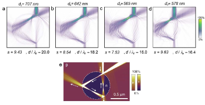
Figure 9 shows a sharper electron beam, focused and collimated by combining a aperture and a parabolic lens, scattering on a VD with various non-scaled diameters and similar ratio . In particular Figure 9a has the same scaled diameter as the VD simulated in many of the structures considered in Boggild2017 , thus comparing well both with respect to the emission jets and the internal, polygonal current resonances. Clearly interference effects are of higher importance in the quantum mechanical calculations, which are seen as beam broadening inside and outside the VD.
In Fig. 10 we show the bond-currents obtained by scanning the beam using different magnetic fields, ranging from to . Also in this case we find a good qualitative agreement with the semi-classical studiesBoggild2017 , capturing both emitted jets and whispering channels within the circular junctions.
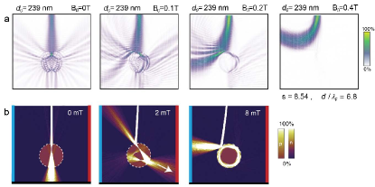
The beam size difference as well as the interference in- and outside the VD are the main differences that amount to the leaking of electrons in the VD. We point out that when we model a large physical system such as that in Fig. 10b with a scaled-down model we have to scale the magnetic field such that the flux is the same. This is done by using the relation , where is the original non-scaled magnetic field Beconcini2016 . In addition to this scaling we make use of larger magnetic fields compared to the semiclassical simulations in Ref. Boggild2017 , in order to access beam scattering off-axis with respect to the VD center. By doing this we compensate the small source/VD distance in our geometry, which could not be further extended due to limits of applicability of the scaling procedure (e.g. see Fig.2 in Beconcini2016 ).
IV Conclusions
In conclusion, we carry out large-scale quantum transport calculations based on simple tight-binding models of graphene and the non-equilibrium Green’s function method. We report on how to include the effects of junctions, magnetic field and complex absorptive potentials into the calculations, as simple perturbative terms to the Hamiltonian. We show how different choices of boundary conditions lead to different current features in the system, setting up local CAP regions in order to minimize artificial interference in the current patterns. We reproduce, from a fully atomistic perspective, some key features of electron transport in a DFM, such as electron beam collimation, deflection and scattering off circular Veselago dots, presenting a direct comparison with the semi-classical results reported in Boggild2017 . As expected, the quantum transport simulations show that current density of structures, which are large compared to the Fermi wavelength, show reasonable resemblance with the classical calculations. On the other hand, it is evident that quantum coherence leads to bond current patterns with richer emission and reflection structures, which may be utilized to extract more detailed information of targets than possible with semi-classical calculations.
V Acknowledgements
We are thankful to Dr. Jose Caridad for discussions. We acknowledge funding from Villum Fonden (grant no. 00013340) and the Danish research council (grant no. 4184-00030). The Center for Nanostructured Graphene (CNG) is sponsored by the Danish Research Foundation, Project DNRF103.
References
References
- [1] Thiti Taychatanapat, Kenji Watanabe, Takashi Taniguchi, and Pablo Jarillo-Herrero. Electrically tunable transverse magnetic focusing in graphene. Nature Physics, 9(4):225–229, apr 2013.
- [2] Luca Banszerus, Michael Schmitz, Stephan Engels, Matthias Goldsche, Kenji Watanabe, Takashi Taniguchi, Bernd Beschoten, and Christoph Stampfer. Ballistic Transport Exceeding 28 m in CVD Grown Graphene. Nano Letters, 16(2):1387–1391, feb 2016.
- [3] Vadim V Cheianov, Vladimir Fal’ko, and B L Altshuler. The focusing of electron flow and a Veselago lens in graphene p-n junctions. Science (New York, N.Y.), 315(5816):1252–5, mar 2007.
- [4] Shaowen Chen, Zheng Han, Mirza M Elahi, K M Masum Habib, Lei Wang, Bo Wen, Yuanda Gao, Takashi Taniguchi, Kenji Watanabe, James Hone, Avik W Ghosh, and Cory R Dean. Electron optics with p-n junctions in ballistic graphene. Science (New York, N.Y.), 353(6307):1522–1525, sep 2016.
- [5] Peter Bøggild, José M Caridad, Christoph Stampfer, Gaetano Calogero, Nick Rübner Papior, and Mads Brandbyge. A two-dimensional Dirac fermion microscope. Nature Communications, 8:15783, 2017.
- [6] Arthur W. Barnard, Alex Hughes, Aaron L. Sharpe, Kenji Watanabe, Takashi Taniguchi, and David Goldhaber-Gordon. Absorptive pinhole collimators for ballistic Dirac fermions in graphene. Nature Communications, 8:15418, may 2017.
- [7] F Miao, S Wijeratne, Y Zhang, U C Coskun, W Bao, and C N Lau. Phase-coherent transport in graphene quantum billiards. Science (New York, N.Y.), 317(5844):1530–3, sep 2007.
- [8] Fabian Lackner, Iva Březinová, Joachim Burgdörfer, and Florian Libisch. Semiclassical wave functions for open quantum billiards. Physical Review E, 88(2):022916, aug 2013.
- [9] Thiti Taychatanapat, Jun You Tan, Yuting Yeo, Kenji Watanabe, Takashi Taniguchi, and Barbaros Özyilmaz. Conductance oscillations induced by ballistic snake states in a graphene heterojunction. Nature Communications, 6(1):6093, dec 2015.
- [10] Jürgen Wurm, Klaus Richter, and İnanç Adagideli. Edge effects in graphene nanostructures: Semiclassical theory of spectral fluctuations and quantum transport. Physical Review B, 84(20):205421, nov 2011.
- [11] L. W. Molenkamp, A. A. M. Staring, C. W. J. Beenakker, R. Eppenga, C. E. Timmering, J. G. Williamson, C. J. P. M. Harmans, and C. T. Foxon. Electron-beam collimation with a quantum point contact. Physical Review B, 41(2):1274–1277, jan 1990.
- [12] José M. Caridad, Stephen Connaughton, Christian Ott, Heiko B. Weber, and Vojislav Krstić. An electrical analogy to Mie scattering. Nature Communications, 7:12894, sep 2016.
- [13] Yuhang Jiang, Jinhai Mao, Dean Moldovan, Massoud Ramezani Masir, Guohong Li, Kenji Watanabe, Takashi Taniguchi, Francois M. Peeters, and Eva Y. Andrei. Tuning a circular p-n junction in graphene from quantum confinement to optical guiding. Nature Nanotechnology, 12(11):1045–1049, sep 2017.
- [14] A. H. Castro Neto, F. Guinea, N. M. R. Peres, K. S. Novoselov, and A. K. Geim. The electronic properties of graphene. Reviews of Modern Physics, 81(1):109–162, jan 2009.
- [15] Luis E. F. Foa Torres, Stephan Roche, and Jean Christophe Charlier. Introduction to graphene-based nanomaterials: from electronic structure to quantum transport. Cambridge University Press, New York.
- [16] V. Meunier, A.G. Souza Filho, E.B. Barros, and M.S. Dresselhaus. Physical properties of low-dimensional s p 2 -based carbon nanostructures. Reviews of Modern Physics, 88(2):025005, may 2016.
- [17] Ming-Hao Liu and Klaus Richter. Efficient quantum transport simulation for bulk graphene heterojunctions. PHYSICAL REVIEW B, 86(222):115455, 2012.
- [18] Ming-Hao Liu, Peter Rickhaus, Péter Makk, Endre Tóvári, Romain Maurand, Fedor Tkatschenko, Markus Weiss, Christian Schönenberger, and Klaus Richter. Scalable Tight-Binding Model for Graphene. Physical Review Letters, 114(3):036601, jan 2015.
- [19] M Beconcini, S Valentini, R Krishna Kumar, G H Auton, A K Geim, L A Ponomarenko, M Polini, and F Taddei. Scaling approach to tight-binding transport in realistic graphene devices: The case of transverse magnetic focusing. PHYSICAL REVIEW B, 94:115441, 2016.
- [20] M D Petrović, S P Milovanović, and F M Peeters. Scanning gate microscopy of magnetic focusing in graphene devices: quantum versus classical simulation. Nanotechnology, 28(18):185202, may 2017.
- [21] Samuel W Lagasse and Ji Ung Lee. Understanding magnetic focusing in graphene p-n junctions through quantum modeling. PHYSICAL REVIEW B, 95:155433, 2017.
- [22] Andreas Uppstu. Electronic properties of graphene from tight-binding simulations. PhD thesis, Aalto University, 2014.
- [23] P. V. Buividovich and M. I. Polikarpov. Monte Carlo study of the electron transport properties of monolayer graphene within the tight-binding model. Physical Review B, 86(24):245117, dec 2012.
- [24] Géza I. Márk, Gyöngyi R. Fejér, Péter Vancsó, Philippe Lambin, and László P. Biró. Electronic Dynamics in Graphene and MoS2 Systems. physica status solidi (b), 254(11):1700179, nov 2017.
- [25] Péter Vancsó, Géza I. Márk, Philippe Lambin, Alexandre Mayer, Chanyong Hwang, and László P. Biró. Effect of the disorder in graphene grain boundaries: A wave packet dynamics study. Applied Surface Science, 291:58–63, feb 2014.
- [26] Viktor Krueckl and Tobias Kramer. Revivals of quantum wave packets in graphene. New Journal of Physics, 11(9):093010, sep 2009.
- [27] Victor Häfner. Large scale simulation of wave-packet propagation via Krylov subspace methods and application to graphene. PhD thesis, Institut für Theorie der Kondensierten Materie, Institut für Nanotechnologie, Karlsruhe Institute of Technology, 2011.
- [28] Frank Ortmann, Alessandro Cresti, Gilles Montambaux, and Stephan Roche. Magnetoresistance in disordered graphene: The role of pseudospin and dimensionality effects unraveled. EPL (Europhysics Letters), 94(4):47006, may 2011.
- [29] Aurélien Lherbier, Simon M.-M. Dubois, Xavier Declerck, Yann-Michel Niquet, Stephan Roche, and Jean-Christophe Charlier. Transport properties of graphene containing structural defects. Physical Review B, 86(7):075402, aug 2012.
- [30] Jose E Barrios Vargas, Jesper Toft Falkenberg, David Soriano, Aron W Cummings, Mads Brandbyge, and Stephan Roche. Grain boundary-induced variability of charge transport in hydrogenated polycrystalline graphene. 2D Materials, 4(2):025009, 2017.
- [31] L. Calderín, V.V. Karasiev, and S.B. Trickey. Kubo-Greenwood electrical conductivity formulation and implementation for projector augmented wave datasets. Computer Physics Communications, 221:118–142, dec 2017.
- [32] Mikko M. Ervasti, Zheyong Fan, Andreas Uppstu, Arkady V. Krasheninnikov, and Ari Harju. Silicon and silicon-nitrogen impurities in graphene: Structure, energetics, and effects on electronic transport. Physical Review B, 92(23):235412, dec 2015.
- [33] Mikkel Settnes, Stephen R Power, Jun Lin, Dirch H Petersen, and Antti-Pekka Jauho. Patched Green’s function techniques for two-dimensional systems: Electronic behavior of bubbles and perforations in graphene. PHYSICAL REVIEW B, 91:125408, 2015.
- [34] Supriyo Datta. Nanoscale device modeling: the Green’s function method. Superlattices and Microstructures, 28(4):253–278, oct 2000.
- [35] Y. Hancock, A. Uppstu, K. Saloriutta, A. Harju, and M. J. Puska. Generalized tight-binding transport model for graphene nanoribbon-based systems. Physical Review B, 81(24):245402, jun 2010.
- [36] Mads Brandbyge, José-Luis Mozos, Pablo Ordejón, Jeremy Taylor, and Kurt Stokbro. Density-functional method for nonequilibrium electron transport. Physical Review B, 65(16):165401, mar 2002.
- [37] Nick Rübner Papior, Nicolás Lorente, Thomas Frederiksen, Alberto García, and Mads Brandbyge. Improvements on non-equilibrium and transport Green function techniques: The next-generation transiesta. Computer Physics Communications, 212:8–24, mar 2017.
- [38] Nick Rübner Papior. sisl: v0.9.2, 2018.
- [39] Nick Rübner Papior, T. Gunst, D. Stradi, and M. Brandbyge. Manipulating the voltage drop in graphene nanojunctions using a gate potential. Physical Chemistry Chemical Physics, 18(2), 2016.
- [40] Nick Rübner Papior. Computational Tools and Studies of Graphene Nanostructures. PhD thesis, Technical University of Denmark, 2016.
- [41] José M Soler, Emilio Artacho, Julian D Gale, Alberto García, Javier Junquera, Pablo Ordejón, and Daniel Sánchez-Portal. The SIESTA method for ab initio order-N materials simulation. Journal of Physics: Condensed Matter, 14(11):2745–2779, mar 2002.
- [42] Arash A. Mostofi, Jonathan R. Yates, Giovanni Pizzi, Young-Su Lee, Ivo Souza, David Vanderbilt, and Nicola Marzari. An updated version of wannier90: A tool for obtaining maximally-localised Wannier functions. Computer Physics Communications, 185(8):2309–2310, aug 2014.
- [43] Hang Xie, Yanho Kwok, Feng Jiang, Xiao Zheng, and Guanhua Chen. Complex absorbing potential based Lorentzian fitting scheme and time dependent quantum transport. The Journal of Chemical Physics, 141(16):164122, oct 2014.
- [44] Zhizhou Yu. First-principles study on transient dynamics of nanodevices. PhD thesis, The University of Hong Kong, 2015.
- [45] Zhengfei Wang and Feng Liu. Manipulation of Electron Beam Propagation by Hetero-Dimensional Graphene Junctions. ACS Nano, 4(4):2459–2465, apr 2010.
- [46] Ming-Hao Liu, Cosimo Gorini, and Klaus Richter. Creating and Steering Highly Directional Electron Beams in Graphene. Physical Review Letters, 118(6):066801, feb 2017.
- [47] József Cserti, András Pályi, and Csaba Péterfalvi. Caustics due to a Negative Refractive Index in Circular Graphene p-n Junctions. Physical Review Letters, 99(24):246801, dec 2007.
- [48] J. M. Luttinger. The Effect of a Magnetic Field on Electrons in a Periodic Potential. Physical Review, 84(4):814–817, nov 1951.
- [49] Jesper Goor Pedersen and Thomas Garm Pedersen. Tight-binding study of the magneto-optical properties of gapped graphene. Physical Review B, 84(11):115424, sep 2011.
- [50] Christoph W Groth, Michael Wimmer, Anton R Akhmerov, and Xavier Waintal. Kwant: a software package for quantum transport. New Journal of Physics, 16(6):063065, jun 2014.
- [51] Shinji Nonoyama and Akira Oguri. Direct calculation of the nonequilibrium current by a recursive method. Physical Review B, 57(15):8797–8800, apr 1998.
- [52] Gemma C. Solomon, Carmen Herrmann, Thorsten Hansen, Vladimiro Mujica, and Mark A. Ratner. Exploring local currents in molecular junctions. Nat Chem, 2(3):223–228, mar 2010.
- [53] L. P. Zârbo and B. K. Nikolić. Spatial distribution of local currents of massless Dirac fermions in quantum transport through graphene nanoribbons. Europhysics Letters (EPL), 80(4):47001, nov 2007.
- [54] Douglas J. Mason, Mario F. Borunda, and Eric J. Heller. Semiclassical deconstruction of quantum states in graphene. Physical Review B, 88(16):165421, oct 2013.
- [55] Claudia Gomes da Rocha, Riku Tuovinen, Robert van Leeuwen, and Pekka Koskinen. Curvature in graphene nanoribbons generates temporally and spatially focused electric currents. Nanoscale, 7(18):8627–8635, apr 2015.
- [56] Thijs Stuyver, Nathalie Blotwijk, Stijn Fias, Paul Geerlings, and Frank De Proft. Exploring Electrical Currents through Nanographenes: Visualization and Tuning of the through-Bond Transmission Paths. ChemPhysChem, 18(21):3012–3022, nov 2017.
- [57] Daijiro Nozaki and Wolf Gero Schmidt. Current density analysis of electron transport through molecular wires in open quantum systems. Journal of Computational Chemistry, 38(19):1685–1692, jul 2017.
- [58] R. L. Heinisch, F. X. Bronold, and H. Fehske. Mie scattering analog in graphene: Lensing, particle confinement, and depletion of Klein tunneling. Physical Review B, 87(15):155409, apr 2013.
- [59] Neetu Agrawal (Garg), Sankalpa Ghosh, and Manish Sharma. Scattering of massless Dirac fermions in circular p-n junctions with and without magnetic field. Journal of Physics: Condensed Matter, 26(15):155301, apr 2014.