Signatures of van Hove singularities probed by the supercurrent in a graphene - hBN superlattice - supplementary materials
1 Additional information about the sample
1.1 Fabrication
A dry pick-up technique developed by Zomer et al. [1] was applied to encapsulate the graphene in between two hBN flakes. Graphene and hexagonal Boron Nitride (hBN) flakes were exfoliated (Nitto tape) onto p-doped silicon wafer with a thermally grown 300 thick SiO2 layer. The used hBN crystals were grown by K. Watanabe and T. Taniguchi and the graphite source was HOPG from ”HQ-graphene”. The stack was annealed in a H2/N2 atmosphere for 50 min at 300 ∘C. The contacts were defined by e-beam lithography using 300 nm thick PMMA. After cold development (at 0∘C) in IPA/DI-water (7:3), the graphene was contacted using reactive ion etching process with a gas mixture of SF6, O2 and Ar to open an access to the encapsulated graphene, which then was contacted in a quasi four terminal configuration with sputtered MoRe (1:1) leads (thickness 50 nm). The liftoff was performed in warm (50 ∘C) acetone. In an additional lithography step the MoRe was contacted by Ti/Au (5 nm/50 nm) and bond pads were defined. In the end the width of the transport channel was defined using the same reactive ion etching process as mentioned before.
1.2 Determination of the superlattice wavelength
When the crystallographic axis of a graphene layer is aligned (or almost) with the one of a hexagonal Boron Nitride (h-BN) layer, because the two lattices have almost the same lattice constant (with a mismatch of [2]), a moiré superlattice formes (see fig. 1 (a)). This hexagonal superlattice is characterised by its wavelength and the corresponding wavevector [3].
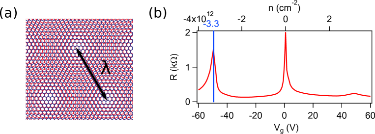
Secondary Dirac points are expected to arise at the new Brillouin zone boundaries, at vectors such that . In a 2D material, k can be expressed as a function of the charge carrier density by , such that the wavelength can be obtained from the position of the second Dirac peak : . In our sample, is extracted from the normal state resistance measurement of fig. 1, giving .
The maximum value of is of the order of , corresponding to a perfect alignment of the lattices, and decreases with the misalignement angle. This misalignement angle , expressed in radian, can be estimated from the following formula [4]:
| (1) |
with the lattice constant . In our sample, we get .
1.3 Temperature dependence of the normal state resistance
In some monolayer graphene h-BN superlattice, a gap opening has been predicted and observed [4, 5, 6], leading presumably to edge currents [7]. In order to determine if there is a gap opening in the density of states of our sample, we measure the resistivity as a function of temperature, represented in fig. 2. One can see that, below , the resistivity only slightly varies. Note as well that the value of the resistivity is not as high as one would expect if there would be a gap [5].

If there is a gap, it should be equal to twice the thermal activation energy extracted from an Arrhenius plot. Namely, by plotting the logarithm of the resistivity as a function of , where is the temperature, one expects a linear behavior with a slope of . From fig. 2 (b), this linear behavior is not observed in our sample, except at large temperature () corresponding to an activation energy of 110 K, and thus a gap of 220 K. The extracted energy has to be compared with the disorder energy at the DP. This disorder manifests itself in charge puddles, which appear in our sample at charge carrier densities smaller then , corresponding to a energy of . It is thus possible that there exists a gap in the system, maybe induced by the superlattice, which would be smeared out by disorder at low temperature. If so, it anyway doesn’t affect the measurements of the main text, which are only performed below 100 mK.
1.4 Quantum Hall effect

After the measurements described in the main text, the sample has been reshaped using a SF6 etching recipe. The new width, gives for sample E an aspect ratio close to 1, which is more appropriate for observing quantum Hall plateaus in a two terminal geometry [8]. Fig. 3 shows the differential conductance of sample E as a function of the gate voltage and the magnetic field at a temperature of . This measurement, showing a clear plateau at , confirms that the measured sample is a monolayer graphene.
One can also see a well defined plateau at and faintly defined ones between 2 and at 8 T. This shows that some degeneracies are lifted, especially for hole doping (where the sample is cleaner)[9]. This breaking of degeneracy at rather low field in a not-so-clean sample could be attributed to the superlattice [10, 11]. The spacing between the split Landau levels is then four time smaller, which may be the reason why the plateaus are blurred.
The features observed at larger gate voltage are strongly affected by the superlattice band structure of the sample, their detailed investigation would require a Hall bar measurement and is far beyond the scope of this work.
2 Electronic transport
2.1 Transport regime
2.1.1 Contact resistance and mean free path
We estimated the mobility of the graphene device and the contact resistance at the interface with MoRe by fitting the conductivity as a function of carrier density using
| (2) |
where is the electron charge, the residual conductivity at the charge neutrality point and corresponds to a carrier density independent contribution to the resistivity from contact resistance and short range scattering. Note that this procedure is valid only in the vicinity of the charge neutrality point and becomes irrelevant close to the satellite Dirac point (ie for ), which limits the range of the fit and thus the reliability of the results. Still, in order to give an order of magnitude of the quality of the sample, and are listed for the four samples in Tab.1.
To decide if our samples are diffusive or not, we have to estimate their mean free path. For that, we relate the diffusion coefficient to the density of states through the Einstein relation . Then, assuming that the density of state is the one of a graphene monolayer (which is approximately true for a superlattice around the main DP), we get (independently of the value of the Fermi velocity):
| (3) |
The values of the mean free paths for each junction is estimated in table 1 for a charge carrier density of (when two values are given, they correspond to hole and electron doping respectively).
| Sample | L () | ||||
|---|---|---|---|---|---|
| B | 450 | 60/35 | 0.1 | 315/350 | 7’500/4’000 |
| C | 640 | 115/85 | 0.15 | 137/193 | 14’000/12’000 |
| D | 820 | 190/120 | 0.2 | 80/92 | 30’000/11’000 |
| E | 1000 | 230/150 | 0.2 | 102/137 | 37’000/22’000 |
From this table, the four samples are diffusive (). The is proportional to and therefore it depends only weakly on for high doping. Moreover, in the vicinity of the satellite Dirac points, the mean free path may decrease again, such that the sample stays in the diffusive regime all over the investigated range of gate voltage. The mobility is unusually low for a hBN stack, and the smaller is the junction, the more diffusive it is. This may be due to the close proximity of the MoRe contacts, which deteriorates the quality of the sample.
2.1.2 Long or short junction?
It is important to know if our junctions are in a short or a long junction regime regarding the superconducting proximity effect. In a short junction, one can neglect the phase acquired by the Andreev pair during the propagation in the junction compared with the phase acquired in the Andreev reflection. This short junction regime corresponds to
| (4) |
with (value estimated from multiple Andreev reflections, see below) and (in a superlattice, it may be smaller, so this value is an upper bound). In our samples, , so we are in the long junction regime.
In the diffusive limit, the coherence length is actually , which gives similar order of magnitude (see table 1, where it has been estimated as well with ).
2.2 Supercurrent measurement
2.2.1 Additional information about the estimation of the DOS from product
and for the four junctions investigated
We show on fig. 4 the normal state resistance and the critical current as a function of gate voltage for the four junctions measured. The resistance plotted is the measured one, including the contact resistance.
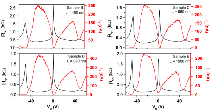
Fig. 5 shows the product of the normal state resistance with the critical current .
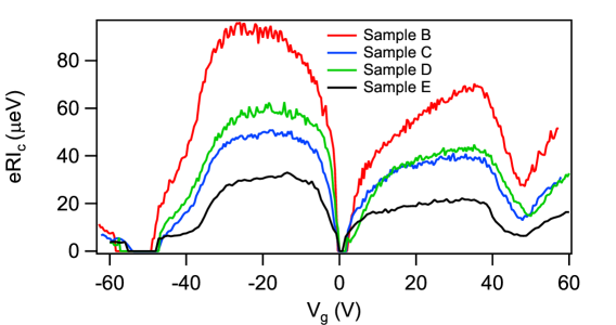
Determination of the DOS
As explained in the main text, in a long and diffusive Josephson junction, the density of state can be expressed as a function of the critical current and of the normal state resistance through:
| (5) |
is defined such that and is not known a priori in graphene [12, 13]. The contact resistance is not known precisely as well. These two parameters are thus taken as gate-independent fitting parameters that we adjust manually to obtain a good agreement with the calculated DOS. The obtained values are given in table 2.
| Sample | L () | ||
|---|---|---|---|
| B | 0.45 | 275-320 | 0.75-0.7 |
| C | 0.64 | 115-150 | 0.4 |
| D | 0.82 | 80-100 | 0.45 |
| E | 1 | 75-110 | 0.3-0.27 |
Note that this calculated DOS is obtained by setting some parameters that we cannot determine experimentally and may be altered by the disorder in the sample. For these reasons, added to the fact that our measurement of supercurrent is not reliable close to the Dirac point, the agreement is more qualitative than quantitative. Consequently, we estimate the uncertainty on the given values of and to be of the order of 10%.
2.2.2 Switching/critical current
In a finite temperature measurement, one doesn’t measure exactly the critical current of the Josephson junction but rather what is called a switching current, resulting from the thermal activation of the switching to the non-superconducting state. This point is important for the estimation of the density of states as described in the main text, where we assumed that the measurement represented the real critical current.
To quantify this thermal effect, we use the resistively and capacitively shunted junction (RCSJ) model. It consists in modelling the Josephson junction as a perfect Josephson element with a sinusoidal current-phase relation (for graphene, this is a reasonable assumption), in parallel with a resistance and a capacitor. The whole system is biased by a current and is the voltage across it.

Using the Josephson relation and Kirchhoff’s current law, we write [14]:
| (6) |
with and . This is formally the equation of motion of a particle, whose position is given by , in an effective potential (fig. 6):
| (7) |
and subjected to a frictional force , with .
At zero temperature , while , the phase is trapped in a local minimum of potential, where it oscillates at frequency . When the current is increased to , there is no barrier preventing the phase from increasing leading to a rapid onset of voltage across the junction. The current becomes dissipative.
At finite temperature, thermal activation allows the fictitious particle to leave its local potential minimum for . This current at which the particle tunnels across the barrier while increasing I is called the switching current , and is always lower than the critical current. To estimate the ratio between the measured switching current and the ”real” critical current, we calculate the barrier [15]:
| (8) |
According to Arrhenius law, the probability of switching (i.e. the probability of overcoming the barrier) is then [16]. For each value of , the value of the current needed to reach a switching probability of 0.5 has been extracted, and is plotted on fig. 6 (b) for an estimated electronic temperature of corresponding to our measurements. We see qualitatively that, if the critical current is higher than , this ratio is roughly constant.
To figure out to what extent the temperature affects our conclusions, we plot on fig. 6 (c) a figure similar to fig. 2 of the main text, where we compare the DOS extracted from the measurement with and without taking into account the finite temperature. Far from the Dirac points, the difference between the two quantities is very tiny, below the uncertainty of the measurement. This is why, in the main text, we used the measured current without applying any correction and called it . At the Dirac point, where the supercurrent cancels, temperature effect may explain the unexpected increase of the DOS, even though our simple model is not able to explain it fully.
Note that, in this qualitative estimation of the effect of finite temperature, we neglected the influence of quantum macroscopic tunnelling [17] and assumed that the sweep velocity of the bias current was infinitely slow.
2.3 Determination of the superconducting gap of MoRe
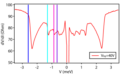
The superconducting gap of MoRe was measured in a different graphene stack, which doesn’t show any transport signatures of a superlattice. To do so, the differential resistance was measured with a standard lock-in technique in a quasi four terminals configuration as a function of voltage bias Vbias and an ac-voltage amplitude of 20 V at 377 Hz. A clear decrease of the differential resistance is observed at Vbias=2.6 meV, that we attribute to twice the superconducting gap of MoRe and indicated by the dark blue line in Fig.7. This value () is of the same order as measured by Borzenets et al. [18] (=1.2 meV). Additional peaks of the differential resistance inside the gap arise due to multiple Andreev reflection MAR at Vbias equal to (light blue), 2/3 (pink) and /2 (violet). In the region around Vbias=0, the dV/dI drops to 0 because of a supercurrent flowing through the JJ as soon as V/RL¡Icm, where RL is the line resistance, since the finite value of RL (RL=137 ) causes an effective current bias of the sample.
3 Analysis of interference patterns: extraction of the current distribution
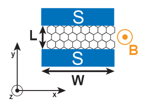
In this section, we describe the procedure used to extract the current distribution from the interference pattern of the critical current as a function of magnetic field , following [19, 20, 21]. We choose the graphene sheet to lie in the x-y plane with contacts along x from -W/2 to W/2, a length of L and an out of plane magnetic field in z-direction.
3.1 Extracting from interference pattern
We assume that the supercurrent in graphene can be described approximately with a sinusoidal current-phase relation, i.e.
| (9) |
where is the maximum supercurrent density and the superconducting phase difference between the two superconductors. This is a very reasonable assumption if most of the transmission channels are not perfectly transmitted (which is more likely the case in our diffusive sample with non-perfect contact resistance) and is consistent with existing measurements in graphene [22, 23].
If a perpendicular magnetic field is applied, two supercurrent paths flowing through the junction pick up an additional relative phase with respect to each other, which depends on the enclosed area by the two paths. Therefore, the superconducting phase at position x is given by the integration of the perpendicular magnetic field over the penetrated area added to a reference phase and is expressed as
| (10) |
where is the flux quantum and the magnetic flux. The area is given by , where the London penetration depth is added twice to the junction length to take a finite penetration of the magnetic field in the contacts in to account.
Therefore the total mediated supercurrent can be calculated by the integration along the sample width W.
| (11) |
with , the even and the odd part of . For a fixed magnetic field B, one can vary to obtain the maximum current known as critical current of the JJ. We assume now an even current distribution, such that the problem simplifies and the measurable quantity can be express as
| (12) |
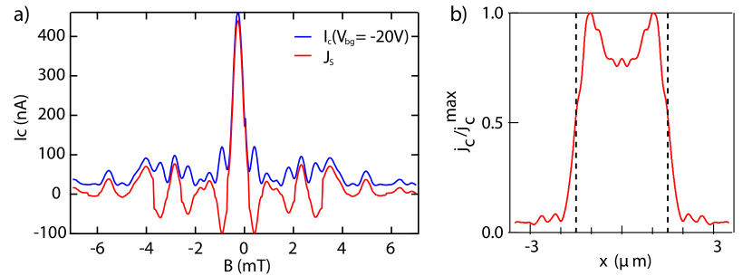
Further, only the even part of the integral will be non zero leaving us with , which can take negative or positive values (with a sign change at each zero crossing in the case of homogeneous current distribution ). The measurement, represented in blue in Fig.9a, is actually , such that we have to reconstruct the sign of . This is done by inverting the sign of every second lobe of (see Fig.9a). To prevent discontinuities, we subtracted a constant background from to shift its value to 0 for magnetic fields of 6 mT. This background arises partly due to the used measurement method described in the main article.
By calculating the inverse Fourier transform of the current density in real space can be determined as
| (13) |
The result of the described procedure is shown in Fig.9b.
3.2 Adding an odd component to the current distribution
The non vanishing critical current at the minima of the interference pattern is an indication for a contribution of an odd part in the current distribution . Taking into account a new expression for is given by
| (14) |
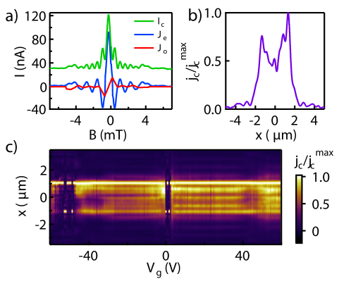
The critical current can now be written as , where and are the even and odd part of . From the measured interference pattern we see the even part dominates most of the time. But, from Eq.14, it follows that the odd part is dominating where vanishes, i.e. for small . To reconstruct the odd contribution we followed the Ansatz in Ref.[21] interpolating between the minima of and flipping sign between each lobe (see Fig.10a). The result of is shown in Fig.10b). We observe that it seems that one edge is contributing more to the supercurrent transport than the other. As described in the main article we are able to extract the density of states (DOS) of the bulk by extracting the dependence of the critical current with carrier density from the calculated current density as a function of gate shown in Fig.10c. No qualitative difference in the resulting DOS was observed between the calculation with and without the odd component .
This analysis containing even more assumption, we rather limit ourselves to the even component, as describe in section 3.1.
3.3 Interference pattern for sample C

In addition to the current distribution of sample D (L=0.82 m), which is discussed in the main article, we also studied the one in sample C (L=0.64 m). The interference pattern as a function of gate voltage and magnetic field was measured and normalized as described for sample D (see Fig.11a). It shows a monotonous behaviour over the entire gate range. Small changes appear at the satellite Dirac points at positive gate voltage, which are probably due to the strongly reduced amplitude of the critical current, such that small features can not be resolved anymore due to the limited measurement resolution. The calculation of the current density does not carry any indication of a increased edge to bulk current ratio around the van Hove singularities. This behaviour is consistent with the observation that the estimated DOS from of sample C probes the van Hove singularities without additional data processing like for sample D, where a finite current contribution by the edges had to be subtracted.
References
- [1] P. J. Zomer, M. H D Guimarẽs, J. C. Brant, N. Tombros, and B. J. Van Wees. Fast pick up technique for high quality heterostructures of bilayer graphene and hexagonal boron nitride. Applied Physics Letters, 105(1), 2014.
- [2] M. Yankowitz, Jiamin Xue, Daniel Cormode, J. D. Sanchez-Yamagishi, K Watanabe, T Taniguchi, P. Jarillo-Herrero, Philippe Jacquod, and B. J. LeRoy. Emergence of superlattice Dirac points in graphene on hexagonal boron nitride. Nature Physics, 8(5):382–386, 2012.
- [3] L A Ponomarenko, R. V. Gorbachev, G L Yu, D C Elias, R. Jalil, A A Patel, A Mishchenko, A S Mayorov, C. R. Woods, J. R. Wallbank, M. Mucha-Kruczyński, B A Piot, M Potemski, I V Grigorieva, K. S. Novoselov, F. Guinea, V. I. Fal’Ko, and A. K. Geim. Cloning of Dirac fermions in graphene superlattices. Nature, pages 1–4, 2013.
- [4] J. R. Wallbank, A. A. Patel, M. Mucha-Kruczyński, A. K. Geim, and V. I. Fal’ko. Generic miniband structure of graphene on a hexagonal substrate. Physical Review B, 87(24):245408, jun 2013.
- [5] C. R. Woods, L Britnell, a Eckmann, R S Ma, J C Lu, H M Guo, X Lin, G L Yu, Y. Cao, R. V. Gorbachev, A. V. Kretinin, J Park, L a Ponomarenko, M I Katsnelson, Yu N Gornostyrev, K Watanabe, T Taniguchi, C Casiraghi, H-j Gao, A. K. Geim, and K. S. Novoselov. Commensurate–incommensurate transition in graphene on hexagonal boron nitride. Nature physics, 10(April):1–6, 2014.
- [6] Ziwei Dou, Sei Morikawa, Alessandro Cresti, Shu-wei Wang, C. G. Smith, Christos Melios, Olga Kazakova, K Watanabe, T Taniguchi, and Satoru Masubuchi. Imaging bulk and edge transport near the Dirac point in graphene moiré superlattices. pages 4–6, 2017.
- [7] J. Zhu, A. V. Kretinin, M D Thompson, D A Bandurin, S Hu, G L Yu, J Birkbeck, A Mishchenko, I J Vera-Marun, K Watanabe, T Taniguchi, M Polini, J R Prance, K. S. Novoselov, A. K. Geim, and M. Ben Shalom. Edge currents shunt the insulating bulk in gapped graphene. Nature Communications, 8:14552, feb 2017.
- [8] D A Abanin and Leonid S. Levitov. Conformal invariance and shape-dependent conductance of graphene samples. Physical Review B, 78(035416), jul 2008.
- [9] A F Young, C. R. Dean, L. Wang, H. Ren, P. Cadden-Zimansky, K Watanabe, T Taniguchi, J. Hone, K. L. Shepard, and P. Kim. Spin and valley quantum Hall ferromagnetism in graphene. Nature Physics, 8(7):550–556, 2012.
- [10] B. Hunt, J. D. Sanchez-Yamagishi, A F Young, M. Yankowitz, B. J. LeRoy, K Watanabe, T Taniguchi, Pilkyung Moon, M Koshino, P. Jarillo-Herrero, and R. C. Ashoori. Massive Dirac Fermions and Hofstadter Butterfly in a van der Waals Heterostructure. Science, 340(6139):1427–1430, jun 2013.
- [11] Wei Yang, Xiaobo Lu, Guorui Chen, Shuang Wu, Guibai Xie, Meng Cheng, Duoming Wang, Rong Yang, Dongxia Shi, K Watanabe, T Taniguchi, Christophe Voisin, Bernard Plaçais, Yuanbo Zhang, and Guangyu Zhang. Hofstadter Butterfly and Many-Body Effects in Epitaxial Graphene Superlattice. Nano Letters, 16(4):2387–2392, apr 2016.
- [12] Chuan Li, S Guéron, A. Chepelianskii, and H Bouchiat. Full range of proximity effect probed with superconductor/graphene/superconductor junctions. Physical Review B, 94(11):115405, sep 2016.
- [13] C. T. Ke, I. V. Borzenets, A. W. Draelos, Francois Amet, Y. Bomze, Gareth Jones, Monica Craciun, Saverio Russo, Michihisa Yamamoto, S. Tarucha, and Gleb Finkelstein. Critical Current Scaling in Long Diffusive Graphene-Based Josephson Junctions. Nano Letters, 16(8):4788–4791, aug 2016.
- [14] Michael Tinkham. Introduction to superconductivity. McGraw-Hill, Inc., 1996.
- [15] T. A. Fulton and L. N. Dunkleberger. Lifetime of the zero-voltage state in Josephson tunnel junctions. Phys. Rev. B, 9(11):4760, 1976.
- [16] J. Clarke, A N Cleland, M. H. Devoret, Daniel Esteve, and J. M. Martinis. Quantum Mechanics of a Macroscopic Variable: The Phase Difference of a Josephson Junction. Science, 239(4843):992–997, feb 1988.
- [17] M. H. Devoret, J. M. Martinis, and John Clarke. Measurements of Macroscopic Quantum Tunneling out of the Zero-Voltage State of a Current-Biased Josephson Junction. Physical Review Letters, 55(18):1908–1911, oct 1985.
- [18] I. V. Borzenets, Y. Shimazaki, G. F. Jones, M. F. Craciun, S. Russo, Michihisa Yamamoto, and S. Tarucha. High Efficiency CVD Graphene-lead (Pb) Cooper Pair Splitter. Scientific Reports, 6:23051, mar 2016.
- [19] R. C. Dynes and T. A. Fulton. Supercurrent Density Distribution in Josephson Junctions. Phys. Rev. B, 3:3015–3023, 1971.
- [20] Monica T. Allen, Oles Shtanko, Ion Cosma Fulga, A. R. Akhmerov, K Watanabe, T Taniguchi, P. Jarillo-Herrero, L. S. Levitov, and Amir Yacoby. Spatially resolved edge currents and guided-wave electronic states in graphene. Nature Physics, 12(2):128–133, nov 2015.
- [21] Sean Hart, Hechen Ren, Timo Wagner, Philipp Leubner, Mathias Mühlbauer, Christoph Brüne, Hartmut Buhmann, L. W. Molenkamp, and Amir Yacoby. Induced superconductivity in the quantum spin Hall edge. Nature Physics, 10(September):1–10, 2014.
- [22] G. Nanda, J. L. Aguilera-Servin, P. Rakyta, A. Kormányos, R. Kleiner, D. Koelle, K. Watanabe, T. Taniguchi, L. M.K. Vandersypen, and S. Goswami. Current-Phase Relation of Ballistic Graphene Josephson Junctions. Nano Letters, 17(6):3396–3401, 2017.
- [23] Landry Bretheau, Joel I-Jan Wang, Riccardo Pisoni, Kenji Watanabe, Takashi Taniguchi, and Pablo Jarillo-Herrero. Tunnelling spectroscopy of Andreev states in graphene. Nature Physics, 13(May), 2017.