Superconducting transition edge sensors with phononic thermal isolation
Abstract
The sensitivity of a low-noise superconducting transition edge sensor (TES) is determined by the thermal conductance of the support structure that connects the active elements of the device to the heat bath. Low-noise devices require conductances in the range 0.1 to 10 pW K-1, and so have to rely on diffusive phonon scattering in long, narrow, amorphous SiNx legs. We show that it is possible to manufacture and operate TESs having short, ballistic low-dimensional legs (cross section 500 200 nm) that contain multi-element phononic interferometers and ring resonators. These legs transport heat in effectively just 5 elastic modes at the TES’s operating temperature ( 150 mK), which is close to the quantised limit of 4. The phononic filters then reduce the thermal flux further by frequency-domain filtering. For example, a micromachined 3-element ring resonator reduced the flux to 19 % of a straight-legged ballistic device operating at the quantised limit, and 38 % of a straight-legged diffusive reference device. This work opens the way to manufacturing TESs where performance is determined entirely by filtered, few-mode, ballistic thermal transport in short, low-heat capacity legs, free from the artifacts of two level systems.
I Introduction
There is considerable interest in developing superconducting Transition Edge Sensors (TESs)Irwin and Hilton (2005) for astronomy and space science. For ground-based photometric measurements at long wavelengths (3 mm - 300 m), Noise Equivalent Powers (NEPs) of 10-17 WHz-1/2 are required Posada et al. (2015); Westbrook et al. (2016); Li et al. (2016); Bonetti et al. (2011); for space-based measurements and Earth Observation at long wavelengths, NEPs of 10-18 WHz-1/2 are necessary; for space-based measurements with cooled-aperture telescopes at FIR wavelengths, such as SPICA (200 - 30 m) Roelfsema et al. (2012, 2014); Nakagawa et al. (2014); Goldie et al. (2016, 2012), NEPs of 10-19 WHz-1/2 and better are the necessary target. Time and energy resolved photon counting TESs are being developed for the x-ray space telescope Athena (0.2 - 12 keV) Gottardi et al. (2016); den Hartog et al. (2014); Akamatsu et al. (2016); Smith et al. (2016), and for general utilitarian applications at optical wavelengths (1550 - 400 nm) Cabrera et al. (1998); Portesi et al. (2008); Eisaman et al. (2011); Hadfield (2009); Rosenberg et al. (2006).
State-of-the-art TESs have many favourable characteristics, but they also have a number of shortcomings. To achieve low-noise operation, a low thermal conductance ( 0.1 - 10 pW K-1) is needed between the active elements of the device and the heat bath. TESs are usually fabricated on SiNx membranes, and thin ( 200 nm - 1 m), narrow ( 1 - 10 m), long (100 - 700 m) legs patterned into the membrane, using Deep Reactive Ion Etching (DRIE), to achieve the necessary thermal isolation. The lower the target NEP, the lower the thermal conductance required, and this leads to quite extreme geometries. In the case of ultra-low-noise imaging arrays, long legs ( 500 m - 1 mm) prevent tight optical packing, and inefficient optical coupling schemes must be used to minimise the effects of the large pixel-to-pixel spacing. In addition, SiNx is a highly disordered dielectric and contains an abundance of Two Level Systems (TLSs) Anderson, Halperin, and Varma (1972); Phillips (1972); Zink and Hellman (2004). TLSs result in a specific heat that is many hundreds of times higher than the Debye value and, when combined with low thermal conductance, this leads to devices that are too slow for some applications. Also, phonon trapping in long, narrow legs causes localised transport, which results in wide variations (at least 15 %) in the performance of even notionally identical devices on the same wafer.
In a previous paper we demonstrated that it is possible to manufacture SiNx TESs having tiny ballistic support legs ( 200 nm, m, 1 - 4 m) Osman et al. (2014). The thermal conductance and thermal fluctuation noise in these devices was found to be fully predicted by heat transport calculations based solely on the dispersion curves of elastic modes calculated using the bulk elastic constants of the material. Moreover, the uniformity in performance was high as a consequence of having eliminated resonant phonon scattering in the disorder of the material.
At low temperatures ( 150 mK), heat is transported in low-dimensional dielectric bars through a small number of elastic modes. In our ballistic devices Osman et al. (2014), approximately 6-7 modes were excited, which is close to the quantised limit of 4: one compressional, one torsional, and in-plane and out-of-plane flexure. In a subsequent series of experiments Withington et al. (2017), we measured the thermal elastic attenuation length of these modes to be 20 m, and so our short-legged TESs were operating well within the ballistic limit. It can be shown, and was found in practice, that the ballistic, few mode limit corresponds to an NEP of approximately 10-18 WHz-1/2. This NEP cannot be reduced further by increasing the length, because there is no scattering, or reducing the cross section, because we have already reached the quantised limit. The question arises as to whether it is possible to incorporate micromachined phononic filters into the low-dimensional legs of low-noise TESs in order to reduce the NEP below the ballistic quantised limit.
The incorporation of phononic filters would have a number of benefits: First, it should be possible to manufacture low- devices having legs that are significantly shorter than their long-legged diffusive counterparts. Second, the reduction in would be brought about by a phase coherent scattering process, which is likely to have a beneficial effect on the thermal fluctuation noise in the legs, as compared with that generated by a dissipative diffusive process. Third, we would like to manufacture devices using crystalline Si membranes Rostem et al. (2014, 2016), as this would significantly reduce the heat capacity of the device, but the dispersion curves of Si are very similar to those of SiNx, and the elastic attenuation length considerably larger due to the low density of TLSs. Therefore phononic filters are needed if crystalline Si-membrane devices, which would have exceedingly long phonon mean free paths, are to be produced having NEPs of better than 10-18 WHz-1/2.
The objectives of the exploratory work described here were as follows: (i) to determine whether TESs having low-dimensional phononic filters can be manufactured at all; (ii) to develop and compare manufacturing techniques using optical lithography (OL) and electron beam lithography (EBL); (iii) to investigate whether TESs with phononic filters behave in a conventional way; (iv) to determine whether thermal conductance can in practice be reduced significantly below the few-mode quantised limit; and (v) to investigate uniformity in performance between notionally identical devices. The experimental work was based solely on SiNx membranes, but the results give direct information about the likely behaviour of phononic devices based on crystalline Si membranes.
II Theory
II.1 Elastic waves and ballistic thermal power
The thermal flux through a uniform, low-dimensional, ballistic, dielectric bar can be calculated directly from the dispersion curves of the discrete elastic modes Osman et al. (2014). Here we summarise the calculation because it is central to the subject matter of the paper, and because the ballistic limit will be used later for normalising experimental data.
The classical elastic wave equation is
| (1) |
where is the displacement field in Cartesian direction , the fourth-rank stiffness tensor, the mass density, the angular frequency, and the Einstein summation notation has been assumed. Equation (1) can be solved by adopting a general basis for the displacement field,
| (2) |
where is the ’th expansion coefficient of the -directed displacement and is the associated basis function. Equation (2) may be substituted into Eq. (1), and the resulting algebraic equations solved numerically to give the dispersion curves of the propagating modes. Although a variety of basis functions, such as Gaussian-Hermite polynomials, could be used for this purpose, we have found power-series expansions to be particularly effective Nishiguchi, Ando, and Wybourne (1997).
In the case of a homogeneous, isotropic, insulating dielectric such as SiNx, the stiffness tensor simplifies, and the modal calculation requires only the mass density, , Young’s modulus, , and Poisson’s ratio, , of the material, in addition to the height, , and width, , of the bar. Averaging over any specific microstructure in favour of the bulk elastic properties is appropriate given the long dominant phonon wavelengths (1 m) at low temperatures.
Figure 1(a) shows the dispersion profiles of the low-order modes of the experimentally considered geometry 200 nm, 500 nm, with 3.14 g cm-3, 280 GPa and 0.28 Vlassak and Nix (1992); Walmsley et al. (2007); James, Shackelford, and Alexander (2001). With the exception of the four lowest-order modes, all modes have a cut-off frequency that increases as the cross-sectional area is reduced. Each mode can be assigned to one of four 2-dimensional displacement symmetries: compressional, in-plane and out-of-plane flexural, and torsional. The lowest order mode in each group is a principal mode with no cut-off. Propagation of these four principal modes at all frequencies imposes a fundamental lower limit on the power transmitted ballistically along a straight bar, even as its dimensions are reduced such that the higher order modes carry negligible power. This is often called the ‘quantised limit’.
cd 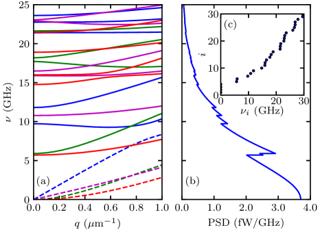
In the context of TESs, each leg consists of a SiNx bar terminating at the central island with a temperature taken to be the superconducting transition temperature , and at the surrounding silicon wafer, held at the bath temperature . The net thermal power transmitted from the island to the heat bath in the ballistic limit is therefore obtained by summing over the power carried by each mode, giving
| (3) |
where is the cut-off frequency of the th mode and
| (4) |
is the single-mode Power Spectral Density (PSD). Previously, we have demonstrated a strong agreement between the net thermal power given by Eq. (3) and measurements on TESs with leg lengths less than 4 m, and a range of widths Osman et al. (2014). This work confirmed that the net power can be calculated from first principles, through the bulk elastic constants, without free parameters, independently of the precise stoichiometry of the SiNx.
Figure 1(b) shows the total net PSD, , summed over all simulated modes, for mK and mK. Sharp discontinuities are evident where individual modes cut on, corresponding to the intercepts of the dispersion curves with the ordinate of Fig. 1(a). At these experimentally representative temperatures, the PSD rolls off such that modes with GHz carry negligible power. Figure 1(c) shows mode number against cut-on frequency , indicating the number of propagating modes as a function of frequency. Above the four principal modes, the number of modes increases quadratically with frequency.
In numerical work, it is convenient to normalise calculated powers to the power carried by a single principal mode, , which defines an effective number of propagating modes:
| (5) |
is the net power that would be carried by a single elastic mode. In the limit of narrow legs operating at low temperatures, the effective number of modes approaches . The experimentally measured power may be substituted for , as is done in Section IV, to calculate the actual effective number of modes propagating in test structures, , for which the ballistic case is an upper limit.
In experimental work, it is convenient to normalise the measured power flowing from the TES island to the heat bath to the straight-leg ballistic limit,
| (6) |
where the factor of 4 arises because each TES has 4 legs. In the case of a phononic thermal filter, quantifies the level of power attenuation achieved relative to the multi-mode ballistic case.
II.2 Phononic interferometers
The central question of this paper is whether it is possible to achieve a significant reduction in thermal flux by introducing phononic filters into low-dimensional dielectric bars. In work on TESs, it is common practice to describe the heat flux in the legs by the equation
| (7) |
where is a parameter that determines the overall magnitude of the flux, and is a parameter that describes the functional dependence on temperature. For truly ballistic transport in a single-mode structure , whereas for ballistic transport in a highly multimode structure Withington, Goldie, and Velichko (2011). In general, for diffusive transport in a few-mode structure, is intermediate between these two values. It follows from Eq. (7) that the differential thermal conductance is given by
| (8) |
Both and change when a phononic filter is introduced, and therefore the flux and thermal conductance can in principle change in different ways. In what follows, we shall measure and directly for a variety of filters.
At first sight, it seems as if a suitable phononic filter might comprise alternating sections of narrow and wide bars, but simulations indicate that is difficult to achieve large acoustic impedance ratios, and the effect on power transmission is relatively small. More troublesome is the fact that the dominant phonon wavelengths at 100 mK are of order 2 m, or shorter, and therefore optical lithography cannot be used easily to define steps that are highly abrupt on a scale size of , diminishing the effectiveness of the filter.
An alternative approach is to make the legs wider and introduce periodic patterns of holes, thereby creating a truly phononic lattice Maldovan (2015); Yi and Youn (2016); Anufriev et al. (2017). Such phononic crystals have been employed, for example, as support structures for micro-mechanical resonators, to reduce coupling loss due to elastic wave propagation to the substrate Mohammadi et al. (2009); Hsu et al. (2011); Feng et al. (2014). Although this approach produces good filter characteristics, the number of transmission channels available, prior to the filter characteristic being applied, is high. Another way of thinking about this same problem is that the phononic lattice comprises a large number of low-dimensional links, each of which transports at least 4 modes. Thus the filter characteristic must compensate for the large increase in the number of underlying modes simply to break even.
We have taken a different approach based on few-mode elastic interferometers and ring resonators: An interferometer is formed by dividing a leg into two paths, one of which is longer than the other. Simulations based on multimode travelling wave calculations Osman (2016) indicate that flux reductions of 25-75 % are possible, depending on the number of interferometers used in series. We have measured the thermal elastic attenuation length in SiNx to be 20 m, and given that this is much larger than a typical wavelength, individual filters behave in a phase coherent way. Large series arrays of interferometers, however, become comparable to the attenuation length, and so operate in the diffusive to ballistic transition. To some extent, absorption isolates the effects of one interferometer on another. In other words, locally the structure behaves as a phase-coherent few-element filter, but globally, the structure conducts diffusively and behaves phase incoherently.
For the purposes of this paper, we define interferometers to be two-path elements that divide and recombine the travelling waves gradually. Another option is a ring resonator design, in which case one benefits from the modal scattering that takes place at the junctions, as well as the interferometric effects of the ring.
II.3 Effective thermal response time
In the results that follow we report direct measurements of thermal fluxes in multi-stage interferometers and ring resonators patterned into the low-dimensional legs of SiNx TESs. Furthermore, as an additional indicator of reduction in thermal differential conductance, we also measure the time constants of phononic devices.
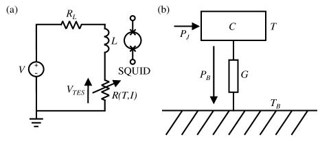
The effective thermal time constant of a TES may be determined from its response to a small step in bias voltage. The induced current response may be derived from the coupled differential equations that describe the TES electrical and thermal circuits. Figure 2(a) shows a Thévenin-equivalent representation of a bias circuit connected to a TES having a current and temperature dependent resistance , where the current is read out using an inductively coupled SQUID circuit. is the sum of the bias and stray resistances, and represents the input inductance of the SQUID and any additional stray inductance due to wiring. Figure 2(b) shows a representation of the thermal circuit, where to a first approximation, the TES has a single heat capacity, , coupled to the heat bath via support legs with thermal conductance, . The differential electrical and thermal equations are then
| (9) |
and
| (10) |
respectively. is the temperature of the central island, is the power flow to the heat bath, and is the Joule power dissipated in the TES bilayer. Notice that we distinguish between , which is the critical temperature of the bilayer defined by some point on the superconducting transition, and , which is the temperature of the bilayer as the instantaneous operating point moves up and down the transition.
It is standard practice in TES physics, to expand non-linear terms such as , and to first order in the small-signal limit around the steady state operating point , and , giving Irwin and Hilton (2005)
| (11) |
where , , , and represents a small change in the applied bias voltage. The resistance-temperature and resistance-current sensitivities are given by and respectively. The time constants and represent electrical and thermal time constants. The natural thermal time constant in the absence of electrothermal feedback, , and strictly , is given by .
Adapting the approach of LindemanLindeman (2000); Irwin and Hilton (2005), Eq. (11) may be solved for the specific case of a small step in bias voltage, at , subsequently maintained over the course of a measurement, giving
| (12) |
where are eigenvalues of the matrix in Eq. 11, and . For low inductance, , such that
| (13) | ||||
| (14) |
where is the effective thermal time constant, given by
| (15) |
| (16) |
Equation 16 is a simplified form following the assumptions that and are small such that , and the device is driven from a near-perfect voltage source Irwin et al. (1998); Irwin (1995). The empirical expression was used here, Eq. (7), which is standard in the TES community.
The time constant governs the rate at which the current stabilises after a voltage step has been applied, through the dominant exponential term in Eq. 12. This response time is significantly shortened from its natural value due to negative electrothermal feedback when the TES is voltage-biased in its transition, where . Since is approximately proportional to , a TES with reduced is expected to have a larger , which can be tested experimentally by fitting Eq. 12 to . Measurements of therefore provide an independent, relative measure of the differential thermal conductances of devices, as distinct from the thermal fluxes, assuming of course that the heat capacities of the devices are the same.
III Experiment
Transition Edge Sensors having a variety of patterned phononic legs were fabricated on 200 nm thick, low-stress, amorphous SiNx membranes. Every TES had an identical m MoAu bilayer with 3 gold bars deposited on the upper surface, giving transition temperatures mK. Phononic structures were classified according to the number of filters in series per leg, m, and the filter style. Distinct filter styles were termed either ‘interferometers’ (mI), with pointed elliptical loops connected by collinear microbridges, or ‘ring resonators’ (mR), with typically angled connections intersecting circular rings: Fig. 3. The primary difference between the two styles lies in the way in which power is divided and recombined upon entering and leaving a filter section: see later. A number of straight-leg control devices (mIC) were also fabricated, with lengths equal to the direct end-to-end lengths of the interferometers mI.
In previous work we have always used optical lithography (OL) and reactive ion etching (RIE) to pattern the the SiNx, followed by deep reactive ion etching (DRIE) to release the membrane from its supporting Si substrateGlowacka et al. (2012). Through this method we have been able to fabricate narrow legs, down to 700 nm, with a high degree of reliability and reproducibility. This method was also used to fabricate our previous few-mode ballistic devices, and we have successfully produced prototype interferometers using OL. The devices reported in this paper, however, used EBL and RIE to pattern the membranes. This required the development of direct-write EBL processing to pattern the legs and define the sputtered Nb bias leads. These new techniques then had to be combined with conventional OL to fabricate the main body of the TES. Using this hybrid method, we have been able to fabricate interferometers and ring resonators having leg cross sections of only 300 200 nm, which ensures that only 4 elastic modes are excited in each bar of a structure for temperatures below 100 mK.
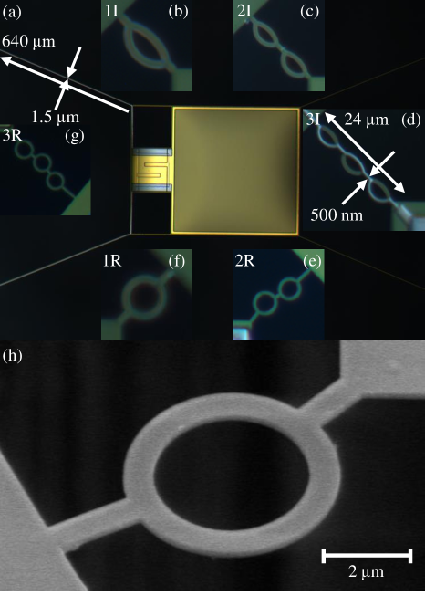
Figure 3(a) shows one of our traditional ultra-low-noise devices having long, straight legs ( 1.5 m, 640 m). The MoAu bilayer, and bars, can be seen as a small gold-coloured square with lateral bars, and the -phase Ta FIR absorber as a large gold-rimmed square. Around the outside of Fig. 3(a), (b - g), we show a number of the phononic filters fabricated. These comprised single, double and triple interferometers and ring resonators, and all of the features had cross sections of 500 200 nm. Table 1 lists the devices tested, with the path difference engineered between the arms of the filters in each phononic leg. Figure 3(d) shows the Nb wiring, for bias and readout, on one of the 3-element interferometers, with an alignment tolerance of 50 nm. Nb is significantly less stiff than SiNx and therefore does not influence the elastic modes of the structure even though its thickness is comparable with that of the SiNx. The superconducting wiring also contributes negligible electronic heat conduction because the quasiparticle density is exceedingly small at low temperatures. Figure 3(h) shows a Scanning Electron Micrograph of a 1R phononic leg, viewed obliquely.
Figure 3 illustrates that it is possible to fabricate few-mode multi-element interferometers, with 500 nm wide features, outstanding definition, and well-aligned Nb wiring. It is remarkable that these tiny patterned legs are perfectly able to support the main body of the TES, and can be fabricated with high yield, which was due in part to our ability to control film stresses in the main body of the device. As will be seen later, it is also notable that these devices performed perfectly well as TESs, with no evidence of anomalous behaviour, such as weak links or additional stray resistance where the Nb leads meandered over the arms of the interferometers. As will be seen later, the thermal properties of these tiny structures were fully consistent with few-mode elastic behaviour even though they were supporting the relatively large central island of the TES. This occurs because the bulk elastic constants are relatively insensitive to static strain, and furthermore the dispersion relationships are insensitive to the bulk elastic constants.
| Device | () | (pW/Kn) | (mK) | (pW/K) | (ms) | |||
|---|---|---|---|---|---|---|---|---|
| 1ICa | - | 2.70 | 22.2 | 141.1 | 0.66 | 2.16 | 3.39 | 0.54 |
| 1ICb | - | 2.53 | 15.4 | 134.5 | 0.62 | 1.81 | 3.13 | 0.64 |
| 2ICa | - | 2.43 | 14.2 | 137.4 | 0.69 | 2.01 | 3.47 | 0.53 |
| 2ICb | - | 2.37 | 12.3 | 133.3 | 0.67 | 1.86 | 3.36 | 0.64 |
| 3ICa | - | 2.28 | 7.5 | 138.3 | 0.48 | 1.36 | 2.42 | 0.85 |
| 1Ia | 1 | 2.74 | 20.1 | 141.4 | 0.55 | 1.84 | 2.83 | 0.60 |
| 1Ib | 1.5 | 2.59 | 13.7 | 131.7 | 0.49 | 1.41 | 2.44 | 0.78 |
| 1Ra | 0 | 2.69 | 15.2 | 137.2 | 0.45 | 1.42 | 2.30 | 1.20 |
| 2Ia | 1, 1.5 | 2.62 | 11.8 | 127.8 | 0.40 | 1.10 | 1.98 | 0.90 |
| 2Ib | 1, 1.75 | 2.67 | 13.3 | 134.5 | 0.41 | 1.25 | 2.07 | 0.73 |
| 2Ra | 1, 1.75 | 2.60 | 8.1 | 127.4 | 0.28 | 0.78 | 1.39 | 1.27 |
| 3Ia | 1, 1.5, 2 | 2.47 | 6.5 | 136.7 | 0.29 | 0.86 | 1.48 | 1.04 |
| 3Ib | 1, 1.25, 1.75 | 2.48 | 6.7 | 133.2 | 0.30 | 0.85 | 1.49 | 1.52 |
| 3Ra | 1, 1.25, 1.75 | 2.44 | 4.0 | 128.5 | 0.19 | 0.51 | 0.94 | 1.88 |
| 3Rb | 1, 1.3, 1.6 | 2.51 | 4.4 | 129.3 | 0.19 | 0.51 | 0.92 | 1.28 |
Each TES was voltage-biased with a low impedance source ( 1.5 m) and read out using a two-stage SQUID amplifier as a low-noise current-to-voltage converter. The TES and SQUID chips were mounted in an optically blackened light-tight box and cooled to a base temperature of 68 mK in an adiabatic demagnetisation refrigerator (ADR). The bath temperature of the TES chip was taken to be that of the copper housing, held constant to within 200 K by means of the residual current in the ADR magnet. Current and voltage offsets and stray resistances were identified and compensated for in data processing. The TES current response to a step in voltage was obtained by biasing the TES in its transition and superimposing a square wave on the bias input, with small amplitude compared to the voltage width of the transition. Current response was averaged over multiple leading-edge voltage steps.
IV Results and Discussion
A TES voltage-biased within its transition self-regulates its temperature due to negative electrothermal feedback. In the steady state, , the net power flow from the island to the heat bath is equal to the Joule power dissipated in the bilayer. The power flow is therefore given by , allowing to be obtained from a series of - curves taken over a range of bath temperatures. If the electrothermal feedback is strong, the TES temperature is essentially constant within the transition at , allowing and to be found.
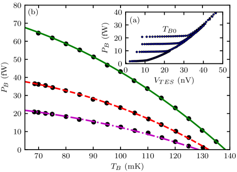
Figure 4(a) shows thermal power against the voltage across the TES, , for device 3Rb, for a set of bath temperatures, . The topmost curve corresponds to the lowest bath temperature used, . The power is essentially constant across the voltage range for which the bilayer is in its transition, indicating the presence of strong electrothermal feedback. This plot is representative of all devices tested, and demonstrates that the presence of the phononic filters in the legs (4 for each device), and associated Nb wiring layer, does not introduce artifacts into the operation of the device.
The power averaged over the transition region is shown in Fig. 4(b) as a function of for devices 3IC (green), 3Ib (red), and 3Rb (magenta). Figure 4(b) displays a clear reduction in the power transmitted through the triple phononic filters relative to the straight leg control, with further improved attenuation for the ring resonator 3Rb over the interferometer 3Ib. This behaviour is reproduced almost identically in devices 3Ia and 3Ra, For all of the devices tested, Eq. (7) was fitted to data of this kind under the assumption that the temperature of the TES was maintained constant at nearly , which is true for sufficiently sharp transitions. , and were free parameters in the fitting process, with corresponding to the intercept of the curve on the axis.
For each device, the measured power at the lowest bath temperature, mK, was used to calculate the normalised power per leg, , according to Eq. 6. In this way, the measured fluxes were normalised to the theoretical ballistic power for a device with straight legs with termination temperatures and . The total thermal conductance of the support structure was determined from Eq. 8. Table 1 lists measured values of , , , , , and .
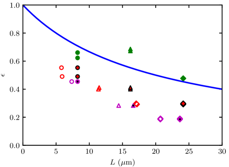
Figure 5 shows the normalised flux against leg length for all of the devices tested. Also shown for comparison (solid blue line) is an analytical model for heat transport in the diffusive to ballistic regime:
| (17) |
In previous workWithington et al. (2017), we determined the acoustic attenuation length, , to be 20 m in SiNx at low temperatures. This was achieved by fitting Eq. (17) to data from a set of straight leg devices having lengths, 1 - 490 m, which span the diffusive to ballistic transition. An of less than unity indicates that a filter has a transmission factor lower than the ballistic case, and an of less than indicates that a filter has a transmission factor lower than its straight-legged counterpart, where some diffusive scattering is present.
In order to compare the flux of a phononic filter with a straight-legged device, it is necessary to assign an equivalent length to the filter, and this can be done in a variety of ways. In Fig. 5, filled markers show the normalised flux as a function of the overall end-to-end length of each phononic leg, equal to the length of the corresponding straight reference legs spanning the same gap. It could be argued, however, that the actual length of the path travelled should be used. For a purely diffusive process, where , the greater path length of a curved leg would reduce relative to a straight leg device with the same end-to-end length irrespective of any coherent destructive process. This should be taken into account, but it is still not clear which path along a multistage filter should be used.
For a fully diffusive process, it is possible to define an equivalent length, , based on the notion of thermal conductances in parallel. In a single interferometer for example, , where and correspond to the straight linking sections and and to the lengths of the different paths around the filter. is therefore a single equivalent length giving the same as a chain of series and parallel conductances representing a phononic structure, for . This constitutes a more appropriate definition of length in Eq. 17 for phononic structures, because it does not mistakenly imply that a reduction in due to the longer path length of the interferometer is necessarily due to coherent interference. The open markers in Fig. 5 show against for all phononic devices. All of the open markers are to the left of the solid markers because the parallel arms reduce the effective length.
The phononic legs show a clear reduction in transmitted power relative both to their corresponding straight leg control devices and the diffusive attenuation expected from Eq. 17. This presents strong evidence that micromachined phononic filters can be used to reduce thermal flux. Moreover, the reductions achieved are comparable with those predicted previouslyOsman (2016). A maximum flux reduction to 19 % of the ballistic limit is achieved for the 3R devices, corresponding to 38 % of the flux in fully diffusive devices. From Eq. 17, a leg length of 87 m would be necessary to achieve this attenuation in the absence of the phononic filter, a more than threefold increase from the 24 m end-to-end length actually used. The expected monotonic decrease in with number of filters per leg is also observed within both the interferometer and ring resonator groups Osman (2016).
Within pairs of devices of the same type, the greatest difference in for different filter path lengths, , is observed between 1Ia and 1Ib, with the larger giving the lower transmission. For devices of type 2I, 3I and 3R, variations in m of the second and third filter stages show negligible effect on . This insensitivity is reasonable since a change in differential path length, , shifts the fringe of the filter, in frequency space, relative to the wide band blackbody spectrum, changing the transmitted flux very little. In the next phase of the work, we will carry out detailed simulations of precise designs in order to understand the degree to which modelling can be used to predict and optimise behaviour.
Figure 5 shows that ring resonators perform significantly better than their interferometer counterparts, for single, double and triple designs, including the case where is the same for the two types. The origin of this improvement is likely to be due to the way in which the principle modes scatter at the junctions. An elastic wave reaching an interferometric filter may maintain its symmetry as it divides between the two arms, whereas in a ring resonator, the incoming wave encounters a perpendicular bar and mode conversion takes place; for example from a torsional wave to two out of phase flexures. Similarly, ring resonators allow waves to propagate multiple times around the ring, possibly contributing to Fabry-Pérot-like enhanced attenuation.
At the lowest bath temperatures, mK, used in this experiment, the effective number of modes transporting heat in a purely ballistic leg is approximately 5, which is very close to the quantised limit of 4. For , from Eq. 17 for in the case of the 3-element ring resonator, the calculated effective number of modes is then 2.5. However, Table 1 shows that for both 3R devices, the effective number of modes is 0.92, from the measured power. Thus the phononic structures have significantly reduced the effective number of modes through frequency-domain filtering.
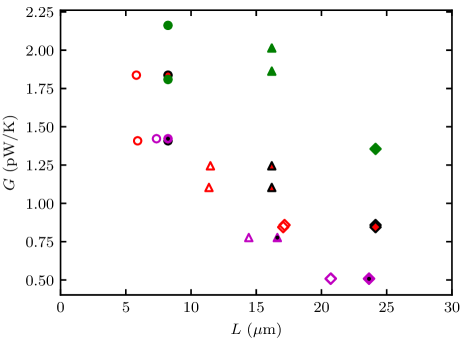
Figure 6 plots the differential conductance against leg length. Indeed the small-signal behaviour of a TES depends on rather than on the absolute value of flux. The trends in conductance are essentially the same as those in flux, with minor differences due to the effect on of variations in between devices. The 2- and 3- stage ring resonators significantly reduce the conductance below the ballistic value of about 2.2 pW K-1. In the case of phononic filters, Table 1 shows that the reduction in and is associated with a reduction in , with staying almost constant. In the ballistic case, we find ,Osman et al. (2014) which is slightly above the single-mode value . In the case of phononic filters, it seems that also. This is very different to the case of long, narrow diffusive legs where takes on values of unity and below, which we have always regarded as being an indicator of the effects of TLS loss in the disordered SiNx Withington et al. (2017).
The values of achieved with few-mode ballistic and phononic legs are already highly suitable for many applications, but in particular it should be noted that if we were to use a 3-stage ring resonator with 50 mK and 100 mK, then 0.3 pW K-1, and we would be close to the requirement pW K-1 for the ultra-low-noise TESs needed for SPICA. Now, however, the legs would only be of order 25 m long, rather than the 600-700 m long legs currently used.
Of particular note is the remarkable consistency in and between different devices of similar design. In fact some of the points on Fig. 5 and Fig. 6 are difficult to distinguish. In conventional TESs having narrow, straight legs, hundreds of microns long, different research teams see conductance variations of or higher between notionally identical devices, even from the same wafer. This variation is attributed to phonon localisation, where elastic waves are reflected by impedance discontinuities due to disorder in the dielectric, creating resonant cells that exaggerate variations in elastic propertiesWithington et al. (2017). The reproducibility seen in Fig. 5 strongly suggests that phononic filters are capable of producing highly uniform arrays, eliminating the troublesome effects of localisation seen in conventional devices.
As an independent indicator of the reduction in , we measured the effective thermal time constants of the phononic TESs. Because all of the TESs were identical, apart from the different leg designs, we would expect the time constants to follow in the appropriate way. Figure 7 shows the change in current, , in response to a small step in bias voltage at for device 3Rb at 90.3 mV, corresponding to a point on the transition where the resistance of the bilayer was 28 % of its normal value. The first dip on the leading edge is due to the electrical response of the TES, and its bias circuit, whereas the slowly rising trailing edge is due to the electrothermal relaxation.
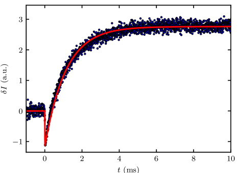
given by Eq. (12) was fitted to the measured data with a scaling pre-factor to give and , corresponding to ms, s and ms, for this particular bias point. The steady state values of , and were taken from - measurements, was assumed, was derived from impedance measurements with the bilayer in its fully superconducting state, and fJ was calculated using the volumes and specific heats of the various materials used. We found that although the values of obtained scale with the value of assumed, the fitted values of obtained do not change; in other words, there is a linear degeneracy between the and , but the same value of always results. Figure 7 is typical of the data taken, and the fit is in good agreement with the model despite using only a single heat capacity .
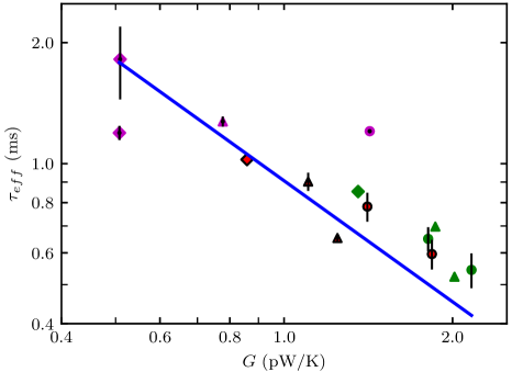
Figure 8 plots against for all of the devices tested. The error bars correspond to the standard error in the plotted mean of multiple measurements of for different bias points across the transition, where applicable for each device. is expected to be approximately inversely proportional to from Eq. (16), and so the simple model is shown as a blue line on Fig. 8. The general agreement offers additional evidence that the phononic filters reduced the differential conductance of the legs in the expected way. There are various reasons why, however, this proportionality may not be exact. The heat capacity will increase slightly as bias voltage is reduced through the transition as the MoAu bilayer becomes increasingly superconducting. Additionally, unknown sources of heat capacity may exist, for example due to residual SiO2 used as an etch stop in fabrication. The steady state values , and vary with bias point, although the impact on between measurements on the same device is typically small. Notwithstanding these considerations, Fig. 8 shows an overall decrease in with increasing , which implies that the interferometrically reduced values of derived through the measured values of and are true differential conductances.
V Conclusions
We have successfully manufactured a range of superconducting transition edge sensors having few mode, phononic thermal isolation in the legs. By using electron beam lithography we were able to pattern interferometers and ring resonators into legs having cross-sectional dimensions of only 500 200 nm. At temperatures of around 100 mK each leg effectively transports heat in just 5 elastic modes, which is close to the quantised limit of 4. The phononic filters then reduced the thermal flux and conductance further. Nb bias leads were patterned on the filters to an alignment tolerance of better than 50 nm. The manufacturing process proved to be highly reliable, giving robust devices with high dimensional definition.
Significant reductions in thermal flux and thermal conductance were recorded, with the ring resonators giving the highest rejection ratios. No artifacts were seen in behaviour, making the devices suitable for many applications. The device-to-device variation in thermal conductance of notionally identical devices was exceedingly small, and well below the 15 % frequently seen in conventional long-legged designs. It should also be noted that the temperature exponent stayed at its near ballistic value of 2.5, in contrast to the case of long narrow legs, where diffusive transport due to two level systems reduces the exponent to typically 1, and below.
A key advantage of phononic filters is that it is possible to approach the very lowest s seen with long ( 700 m) diffusive legs, but using significantly shorter structures. The attenuation length of the low-order modes in SiNx is 20 m, and the ring resonators are typically 5 m in diameter, and therefore by placing a large number of ring resonators in series, dividing a diffusive leg into phase-coherent phononic cells, one would expect to be able to realise thermal conductances significantly smaller than anything achieved to date. Also, one would expect to be able to create ultra-low-noise TESs using crystalline ballistic Si membranes, which would have many advantages.
The next stage in our work will be to carry out a range of scattered travelling wave simulations in diffusive structures in an attempt to identify optimised filters with even higher levels of attenuation. We have already developed a modelling technique for patterned phononic structures operating in the ballistic to diffusive regime, and this will be reported in an upcoming paper.
Acknowledgements.
The authors are grateful to Science and Technology Facilities Council for funding this work. Emily Williams is grateful for a PhD studentship from the NanoDTC, Cambridge, EP/L015978/1.References
- Irwin and Hilton (2005) K. D. Irwin and G. C. Hilton, in Cryogenic particle detection (Springer, 2005) pp. 63–150.
- Posada et al. (2015) C. Posada, P. Ade, Z. Ahmed, K. Arnold, J. Austermann, A. Bender, L. Bleem, B. Benson, K. Byrum, J. Carlstrom, et al., Supercond. Sci. Technol. 28, 094002 (2015).
- Westbrook et al. (2016) B. Westbrook, A. Cukierman, A. Lee, A. Suzuki, C. Raum, and W. Holzapfel, J. Low Temp. Phys. 184, 74 (2016).
- Li et al. (2016) D. Li, J. E. Austermann, J. A. Beall, D. T. Becker, S. M. Duff, P. A. Gallardo, S. W. Henderson, G. C. Hilton, S.-P. Ho, J. Hubmayr, et al., J. Low Temp. Phys. 184, 66 (2016).
- Bonetti et al. (2011) J. Bonetti, A. Turner, M. Kenyon, H. LeDuc, J. Brevik, A. Orlando, A. Trangsrud, R. Sudiwala, H. Nguyen, P. Day, et al., IEEE Trans. Appl. Supercond. 21, 219 (2011).
- Roelfsema et al. (2012) P. Roelfsema, M. Giard, F. Najarro, K. Wafelbakker, W. Jellema, B. Jackson, B. Swinyard, M. Audard, Y. Doi, M. Griffin, et al., in SPIE Astronomical Telescopes+ Instrumentation (Proc. SPIE, 2012) pp. 84420R–84420R.
- Roelfsema et al. (2014) P. Roelfsema, M. Giard, F. Najarro, K. Wafelbakker, W. Jellema, B. Jackson, B. Sibthorpe, M. Audard, Y. Doi, A. di Giorgio, et al., in Proc. SPIE, Vol. 9143 (2014) p. 91431K.
- Nakagawa et al. (2014) T. Nakagawa, H. Shibai, T. Onaka, H. Matsuhara, H. Kaneda, Y. Kawakatsu, and P. Roelfsema, in Proc. SPIE, Vol. 9143 (2014) p. 1.
- Goldie et al. (2016) D. J. Goldie, D. M. Glowacka, S. Withington, J. Chen, P. Ade, D. Morozov, R. Sudiwala, N. Trappe, and O. Quaranta, in Millimeter, Submillimeter, and Far-Infrared Detectors and Instrumentation for Astronomy VIII, Vol. 9914 (Proc. SPIE, 2016) p. 99140A.
- Goldie et al. (2012) D. Goldie, J. Gao, D. Glowacka, D. Griffin, R. Hijmering, P. Khosropanah, B. Jackson, P. Mauskopf, D. Morozov, J. Murphy, et al., in Millimeter, Submillimeter, and Far-Infrared Detectors and Instrumentation for Astronomy VI, Vol. 8452 (Proc. SPIE, 2012) p. 84520A.
- Gottardi et al. (2016) L. Gottardi, H. Akamatsu, M. P. Bruijn, R. Den Hartog, J.-W. den Herder, B. Jackson, M. Kiviranta, J. van der Kuur, and H. van Weers, Nucl. Instrum. Methods Phys. Res 824, 622 (2016).
- den Hartog et al. (2014) R. den Hartog, D. Barret, L. Gottardi, J.-W. den Herder, B. Jackson, P. de Korte, J. van der Kuur, B.-J. van Leeuwen, D. van Loon, A. Nieuwenhuizen, et al., in Space Telescopes and Instrumentation 2014: Ultraviolet to Gamma Ray, Vol. 9144 (Proc. SPIE, 2014) p. 91445Q.
- Akamatsu et al. (2016) H. Akamatsu, L. Gottardi, C. de Vries, J. Adams, S. Bandler, M. Bruijn, J. Chervenak, M. Eckart, F. Finkbeiner, J. Gao, et al., J. Low Temp. Phys. 184, 436 (2016).
- Smith et al. (2016) S. Smith, J. Adams, S. Bandler, G. Betancourt-Martinez, J. Chervenak, M. Chiao, M. Eckart, F. Finkbeiner, R. Kelley, C. Kilbourne, et al., in SPIE Astronomical Telescopes+ Instrumentation (Proc. SPIE, 2016) pp. 99052H–99052H.
- Cabrera et al. (1998) B. Cabrera, R. Clarke, P. Colling, A. Miller, S. Nam, and R. Romani, Appl. Phys. Lett 73, 735 (1998).
- Portesi et al. (2008) C. Portesi, E. Taralli, R. Rocci, M. Rajteri, and E. Monticone, J. Low Temp. Phys. 151, 261 (2008).
- Eisaman et al. (2011) M. Eisaman, J. Fan, A. Migdall, and S. V. Polyakov, Rev. Sci. Instrum. 82, 071101 (2011).
- Hadfield (2009) R. H. Hadfield, Nat. Photonics 3, 696 (2009).
- Rosenberg et al. (2006) D. Rosenberg, S. W. Nam, P. A. Hiskett, C. G. Peterson, R. J. Hughes, J. E. Nordholt, A. E. Lita, and A. J. Miller, Appl. Phys. Lett 88, 021108 (2006).
- Anderson, Halperin, and Varma (1972) P. W. Anderson, B. Halperin, and C. M. Varma, Philos. Mag 25, 1 (1972).
- Phillips (1972) W. Phillips, J. Low Temp. Phys. 7, 351 (1972).
- Zink and Hellman (2004) B. Zink and F. Hellman, Solid State Commun. 129, 199 (2004).
- Osman et al. (2014) D. Osman, S. Withington, D. J. Goldie, and D. M. Glowacka, J. Appl. Phys. 116, 064506 (2014).
- Withington et al. (2017) S. Withington, E. Williams, D. J. Goldie, C. N. Thomas, and M. Schneiderman, J. Appl. Phys. 122, 054504 (2017).
- Rostem et al. (2014) K. Rostem, D. T. Chuss, F. A. Colazo, E. J. Crowe, K. L. Denis, N. P. Lourie, S. H. Moseley, T. R. Stevenson, and E. J. Wollack, J. Appl. Phys. 115, 124508 (2014).
- Rostem et al. (2016) K. Rostem, A. Ali, J. A. Appel, C. L. Bennet, A. Brown, M.-P. Chang, D. T. Chuss, F. A. Colazo, K. L. Denis, T. Essinger-Hileman, et al., in SPIE Astronomical Telescopes+ Instrumentation (Proc. SPIE, 2016) pp. 99140D–99140D.
- Nishiguchi, Ando, and Wybourne (1997) N. Nishiguchi, Y. Ando, and M. Wybourne, J. Phys. Condens. Matter 9, 5751 (1997).
- Vlassak and Nix (1992) J. Vlassak and W. Nix, J. Mater. Res. 7, 3242 (1992).
- Walmsley et al. (2007) B. A. Walmsley, Y. Liu, X. Z. Hu, M. B. Bush, J. M. Dell, and L. Faraone, J. Microelectromech. Syst. 16, 622 (2007).
- James, Shackelford, and Alexander (2001) F. James, F. Shackelford, and W. Alexander, Materials Science and Engineering Handbook, Vol. 49 (CRC press, 2001) pp. 50–52.
- Withington, Goldie, and Velichko (2011) S. Withington, D. Goldie, and A. Velichko, Phys. Rev. B 83, 195418 (2011).
- Maldovan (2015) M. Maldovan, Nat. Mater 14, 667 (2015).
- Yi and Youn (2016) G. Yi and B. D. Youn, Structural and Multidisciplinary Optimization 54, 1315 (2016).
- Anufriev et al. (2017) R. Anufriev, A. Ramiere, J. Maire, and M. Nomura, Nat. Commun 8 (2017).
- Mohammadi et al. (2009) S. Mohammadi, A. A. Eftekhar, W. D. Hunt, and A. Adibi, Appl. Phys. Lett 94, 051906 (2009).
- Hsu et al. (2011) F.-C. Hsu, J.-C. Hsu, T.-C. Huang, C.-H. Wang, and P. Chang, J. Phys. D 44, 375101 (2011).
- Feng et al. (2014) D. Feng, D. Xu, G. Wu, B. Xiong, and Y. Wang, J. Appl. Phys. 115, 024503 (2014).
- Osman (2016) D. Osman, Thermal Transport and Noise in Micro-Engineered Support Structures for Detector Applications, Ph.D. thesis, University of Cambridge (2016).
- Lindeman (2000) M. Lindeman, Microcalorimetry and the Transition-Edge Sensor, Ph.D. thesis, Lawrence Livermore National Laboratory, University of California (2000).
- Irwin et al. (1998) K. D. Irwin, G. C. Hilton, D. A. Wollman, and J. M. Martinis, J. Appl. Phys. 83, 3978 (1998).
- Irwin (1995) K. D. Irwin, Phonon-Mediated Particle Detection using Superconducting Tungsten Transition-Edge Sensors, Ph.D. thesis, Stanford University (1995).
- Glowacka et al. (2012) D. Glowacka, M. Crane, D. Goldie, and S. Withington, J. Low Temp. Phys. 167, 516 (2012).