Magnetic domain texture and the Dzyaloshinskii-Moriya interaction in Pt/Co/IrMn and Pt/Co/FeMn thin films with perpendicular exchange bias
Abstract
Antiferromagnetic materials present us with rich and exciting physics, which we can exploit to open new avenues in spintronic device applications. We explore perpendicularly magnetized exchange biased systems of Pt/Co/IrMn and Pt/Co/FeMn, where the crossover from paramagnetic to antiferromagnetic behavior in the IrMn and FeMn layers is accessed by varying the thickness. We demonstrate, through magneto-optical imaging, that the magnetic domain morphology of the ferromagnetic Co layer is influenced by the Néel order of the antiferromagnet (AFM) layers. We relate these variations to the anisotropy energy of the AFM layer and the ferromagnet-antiferromagnet (FM-AFM) inter-layer exchange coupling. We also quantify the interfacial Dzyaloshinskii-Moriya interaction (DMI) in these systems by Brillouin light scattering spectroscopy. The DMI remains unchanged, within experimental uncertainty, for different phases of the AFM layers, which allows us to conclude that the DMI is largely insensitive to both AFM spin order and exchange bias. Understanding such fundamental mechanisms is crucial for the development of future devices employing chiral spin textures, such as Néel domain walls and skyrmions, in FM-AFM heterostructures.
I Introduction
The field of spintronics Žutić et al. (2004) aims to realize low-power and high-performance next-generation memory Parkin et al. (2008) and logic devices Allwood et al. (2005); Fukami et al. (2009) through the manipulation of the electron spin. Influencing ferromagnet (FM) spins using an antiferromagnet (AFM) is an emerging branch of spintronics Duine (2011); Fukami et al. (2016); Oh et al. (2016); Lau et al. (2016); Tshitoyan et al. (2015). The magnetization in a FM layer can be controlled by an adjacent AFM layer through the interfacial coupling between the two layers Meiklejohn and Bean (1956). AFMs have several other advantages as well. For instance, the net magnetization is zero due to the compensation of magnetic moments at the atomic level. The elimination of stray fields could prove to be vital in integrated devices with low dimensions because such parasitic fields (e.g., from a FM) present complications, such as crosstalk between neighboring devices, susceptibility to external magnetic fields, etc. Furthermore, AFMs possess excellent magneto-transport properties which would allow the generation of large spin currents through which magnetization in an adjacent FM layer could be efficiently switched Tshitoyan et al. (2015); Fukami et al. (2016); Zhang et al. (2016). AFMs also offer dynamics in the terahertz range suitable for ultrafast information processing Satoh et al. (2010).
The exchange interaction is at the heart of magnetic behavior in materials. It comprises a symmetric and an antisymmetric term. The symmetric term, the Heisenberg interaction, prefers collinear orientation of adjacent spins. The antisymmetric term, the Dzyaloshinskii-Moriya interaction (DMI) Dzyaloshinsky (1958); Moriya (1960), prefers canted orientation of neighboring spins. In order to exist, the DMI needs spin-orbit interaction in an asymmetric crystal field, such as in heterostructures lacking spatial inversion symmetry. The DMI gives rise to chiral spin textures Bode et al. (2007); Meckler et al. (2009), which results in many different interesting phenomena Ryu et al. (2013); Schulz et al. (2012). In ultrathin film multilayers, the DMI is of the interfacial form and has been reported to be present at the heavy-metal/ferromagnet (HM/FM) interface Emori et al. (2013); Ryu et al. (2013), at the FM/oxide interface Boulle et al. (2016); Belabbes et al. (2016), and more recently, at the FM/AFM interface Ma et al. (2017). The DMI stabilizes spin structures such as chiral Néel domain walls (DWs) Thiaville et al. (2012) and skyrmions Fert et al. (2013), both of which can be driven as information carriers Parkin et al. (2008); Fert et al. (2017) by electric currents via the spin Hall torque generated in an adjacent HM Liu et al. (2012) and/or AFM Tshitoyan et al. (2015) layer.
In this work, we investigate ultrathin film systems of Pt/Co/IrMn and Pt/Co/FeMn, which exhibit perpendicular magnetic anisotropy (PMA) and perpendicular exchange bias (PEB) Maat et al. (2001); Garcia et al. (2002); Marrows (2003); Sort et al. (2005). These multilayers are potentially of interest because of the coincidence of the DMI with a vertical exchange field that could substitute the need for an externally applied field to stabilize skyrmion bubbles Moreau-Luchaire et al. (2016). We explore the interaction mechanisms at the interfaces, in particular the changes in the magnetic domain texture and the DMI, when going through the paramagnet to AFM phase transition of the AFM layers by systematically varying the thickness of the layers. When the AFM layer is in the paramagnetic phase, the domains of the FM layer are large and contain networks of unreversed narrow domains. As antiferromagnetic order sets in, bubble domains with smooth DWs are nucleated. The DWs eventually become rough at the onset of the exchange bias field. The nucleation density also increases significantly. We relate this variation in the domain morphology to the interplay between the anisotropy energy of the AFM layer and the exchange energy at the interface between the FM and the AFM layers. We identify the Néel and the blocking temperature of IrMn to confirm paramagnetic behavior at low layer thicknesses. We do this by exploiting the previously shown fact Ali et al. (2003a) that these temperatures can be tuned by varying the AFM layer thickness. Finally, we evaluate the interfacial DMI in these systems by Brillouin light scattering (BLS) Nembach et al. (2015); Moon et al. (2013); Di et al. (2015). We measure the DMI at four different phases of the AFM layer: paramagnet phase, AFM phase without exchange bias (EB), AFM phase at the onset of EB, and AFM phase with a large EB. The DMI is similar for all four phases, from which we conclude that there is little influence of AFM spin order or EB on the DMI in these systems. Investigating such interactions provide insight towards the development of future DW and skyrmion devices incorporating an FM-AFM bilayer.
II Multilayer systems
The material systems that we studied consist of Pt(2 nm)/Co(1 nm)/Ir20Mn80(tIrMn) and Pt(2 nm)/Co(0.6 nm)/Fe50Mn50(tFeMn) trilayers deposited on a 5 nm Ta seed layer on a thermally oxidized Si substrate. The Ta seed layer provides a (111) texture for the Pt and Co layers, and consequently, for the IrMn and FeMn layers. Such a crystal orientation is required for IrMn Aley et al. (2008) and FeMn Jungblut et al. (1994) for an effective exchange coupling leading to a large EB. The layers were grown by dc magnetron sputtering at a base pressure of Pa ( Torr) and at an Ar working pressure of 0.33 Pa (2.5 mTorr). A 3 nm capping layer of Pt or Ta was also deposited on top of the stacks in order to prevent oxidation. A change in capping layer has no effect on the magnetic properties we measure here.
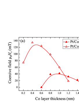
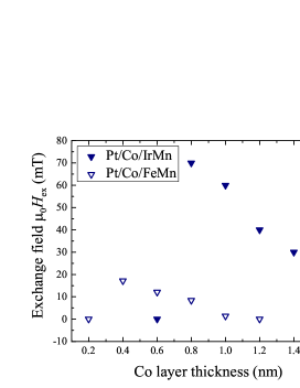
The systems exhibit a uniaxial magnetic anisotropy perpendicular to the plane of the sample. To ensure this, an optimum thickness of Co layer was chosen by systematically varying the thickness for each system. The AFM layer thicknesses were kept constant at 5 nm for IrMn and at 4 nm for FeMn at which the respective systems exhibit an EB field at room temperature. Fig. 1(a) shows coercive fields, obtained from polar MOKE hysteresis loops, as a function of Co layer thickness. PMA could be achieved for a range of Co thicknesses: 0.8-1.4 nm for the IrMn system, and 0.4-1 nm for the FeMn system. Outside this range the sample magnetization lies in-plane. We chose the working Co thickness to be nm for the IrMn system because at this thickness the system exhibits a large coercivity and thus provides a stable perpendicular magnetization. For the same reason, we chose nm for the FeMn system. The magnetization in the Co layer sets the pinning direction of the IrMn or FeMn layer resulting in the PEB. The exchange field decreases while the Co layer thickness increases (Fig. 1(b)) for both systems, in the range where the perpendicular anisotropy is dominant. The PEB is present in the samples in the as-grown state and does not require any post-growth processing.
III Exchange bias and domain morphology in Pt/Co/IrMn
III.1 Magnetic properties
To investigate how the exchange coupling at the FM-AFM interface modifies the domain texture we vary the AFM layer thickness, which dictates the spin order. We first concentrate on the IrMn system of Pt(2 nm)/Co(1 nm)/Ir20Mn80(tIrMn), where the IrMn layer was varied from 1 to 10 nm. A summary of coercive fields () and exchange bias fields () is shown in Fig. 2. These magnetic properties were extracted from hysteresis loops measured by polar magneto-optic Kerr effect (MOKE) magnetometry. is half the difference between the two switching fields, while is the shift of the loop from .
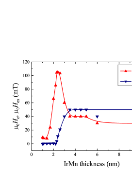
The onset of EB occurs at 2.3 nm of IrMn. rises steadily and stabilizes at mT from 3.5 nm onward. The coercive field peaks at the same 2.3 nm of IrMn at which the exchange field starts to develop. After peaking it gradually drops and settles to a saturation value of mT at the same thickness of 3.5 nm at which the exchange field stabilizes. The trends closely match with those that were reported for similar systems with in-plane magnetization Ali et al. (2003b). The initial increase in coercivity occurs at the onset of the AFM phase of IrMn and start of coupling with the Co layer. At 1 nm layer thickness the IrMn is a paramagnet. As the thickness is increased, the AFM phase sets in and there is an exchange interaction at the Co/IrMn interface. The beginning of this phase transition is marked by the increase in coercivity at 1.7 nm of IrMn. As the Co layer is rotated, it also drags the spins of the IrMn layer along with it, causing an enhancement in coercivity. The Co spins are able to drag the IrMn spins because the volume anisotropy energy (KAFM) of the AFM layer is smaller than the exchange energy (JFM-AFM) at the interface between the FM and the AFM layers (KAFMJFM-AFM). As the IrMn thickness is increased further, KAFM becomes larger, resulting in further enhancement in coercivity until a critical thickness of 2.3 nm is reached when it is no longer energetically favorable for the Co layer to drag the coupled IrMn spins. In other words, from this critical thickness onward, KAFM is large enough to resist the torque from the FM Co layer (KAFMJFM-AFM). Thus, the coercivity gradually decreases while the exchange field starts to increase.
III.2 Domain morphology
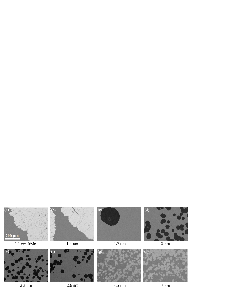
The anisotropy energy of the AFM, and consequently the FM-AFM inter-layer coupling has a profound effect on the domain morphology. Fig. 3 shows the variation in domain structure as a function of IrMn layer thickness. The domains were imaged using a wide-field Kerr microscope in the polar configuration, at which it is sensitive to out-of-plane (OOP) magnetization Hubert and Schäfer (2008). Images captured before and after the application of an OOP field were subtracted, resulting in these difference images. At low IrMn thicknesses, when it is in the paramagnet phase, the domains are large and threaded with disconnected networks of unreversed narrow domains (Fig. 3(a-b)). These narrow domains form as a DW gets pinned at a defect and bends around it. These domains continue to exist since they are bounded by homochiral DWs, which require large fields to annihilate because they have the same chirality due to the DMI, and thus present a topological energy barrier Benitez et al. (2015). At 1.7 nm of IrMn, coupling is initiated due to AFM ordering and the domain morphology changes significantly. Now bubble domains form with relatively smooth DWs instead of the networks of narrow domains as the DWs are no longer pinned at defect sites; Fig. 3(c). This is due to the application of relatively larger fields to nucleate domains and propagate DWs, because of the increase in coercivity of the film brought about by the FM-AFM coupling. It is also because of this enhancement in coercivity that the nucleation density increases significantly with IrMn thickness as even larger fields are now necessary to nucleate domains. This is depicted in Fig. 3(d-e). At the critical thickness of 2.3 nm, the EB field starts to set in and the DWs start to become rough (Fig. 3(e-f)) due to enhanced pinning brought about by the EB, which complicates the spin structure and increases disorder. Eventually, the DWs become even rougher when the system exhibits a stable EB field from 3.5 nm onward as the anisotropy energy of the AFM layer becomes robust; Fig. 3(g-h).
III.3 Investigation of paramagnetic behavior
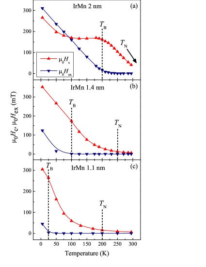
We confirm paramagnetic behavior at low thicknesses by investigating the Néel temperature () and blocking temperature () of the IrMn layer. We do the magnetic characterization in a 2-300 K vibrating sample magnetometer (VSM). For this, we initially cooled the sample from room temperature to 5 K while applying a static perpendicular field of 200 mT, which is large enough to completely saturate the Co layer. Then temperature dependence measurements were done as a series of hysteresis loops at increasing temperatures. Four repeats of field sweep were performed at each temperature to take into account the training effect Ali et al. (2003b) and the last loop was used for characterization. Fig. 4 shows the temperature dependence of (red up triangles) and (blue down triangles) for three of the smaller thicknesses of IrMn (2, 1.4 and 1.1 nm). The thickness of the other layers are as previously. of all the samples falls with temperature and goes to zero at . This is the temperature below which the AFM domains are stable and non-reversible. also shows a downward trend with temperature until , at which temperature there is no AFM ordering and the value of is intrinsic to that of the Co layer. At 2 nm IrMn K, while lies just above room temperature (Fig. 2(a)). With decreasing IrMn thickness, both and shift down the temperature scale, as depicted in Fig. 2(b) and Fig. 2(c) for 1.4 and 1.1 nm of IrMn, respectively. This demonstrates that at low thicknesses, the IrMn layer is, indeed, in the paramagnetic phase and can be made to transit to the AFM phase just by cooling under a field. These experiments also show that and can be tuned easily in this system by controlling the anisotropy energy of the IrMn layer via its thickness.
IV Exchange bias and domain morphology in Pt/Co/FeMn
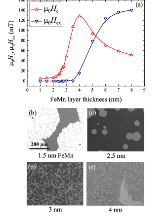
The interaction mechanism, and subsequently the change in the domain structure is similar in the system of Pt(2 nm)/Co(0.6 nm)/Fe50Mn50(tFeMn). Fig. 5 summarizes the dependence of , , and domain morphology on the FeMn layer thickness. The onset of EB occurs at 4 nm of FeMn (Fig. 5(a)) with a peak in coercivity. At 1.5 nm of thickness, the FeMn layer is in the paramagnet phase and the sample exhibit large domains containing network-like features, similar to the IrMn system; Fig. 5(b). At 2.5 nm of FeMn the AFM order sets in, causing an enhancement in coercivity due to FM-AFM inter-layer coupling. We now see the formation of bubble domains with smooth DWs (Fig. 5(c)) and without the network-like features. An increase of the FeMn layer causes the coercivity to increase further resulting in a substantial increases in nucleation density; Fig. 5(d-e).
V Dzyaloshinskii-Moriya Interaction
We turn our attention to quantifying the DMI in these systems, and infer the DW spin texture. The DMI originates at the interface where adjacent spins of the FM undergo a chiral twist due to the exchange interaction mediated by an atom, with a large spin-orbit coupling, from the adjacent HM Emori et al. (2013); Ryu et al. (2013) or AFM Ma et al. (2017) layer. The DMI acts locally on a DW manifesting as an effective in-plane field. This DMI field stabilizes the DW in a chiral Néel configuration Chen et al. (2013); Thiaville et al. (2012) by converting it from the magnetostatically favored Bloch configuration. We measured the DMI using Brillouin light scattering (BLS) spectroscopy Nembach et al. (2015); Moon et al. (2013); Di et al. (2015). In this method, we utilize the non-reciprocity of the DMI-induced frequency-shift and measure the Damon-Eshbach spin-wave frequencies for both field polarities. The frequency shift is then given by
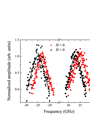
where Deff is the volumetric DMI constant that determines the sign and magnitude of the DMI vector, is the spectroscopic -factor taken to be 2.14 Schoen et al. (2017), Ms is the saturation magnetization, k (with magnitude k) is the wavevector of the spin waves, is the Bohr magneton, and h is Planck constant. The sign of the frequency-shift depends on the direction of the magnetization and the propagation direction of the spin-waves. In the last equality, Ds is the interfacial DMI parameter, which represents the DMI contribution from the top and bottom interfaces ( where is the FM layer thickness). Thus, Ds should be independent of the FM layer thickness, if we consider the DMI to be a truly interfacial effect. Figure 6 shows representative BLS spectra for a sample of Pt(2 nm)/Co(1 nm)/IrMn(2.4 nm), where shifts in Stokes (negative frequencies) and anti-Stokes (positive frequencies) peaks are evident, corresponding to GHz.
The saturation magnetization is measured by a superconducting quantum interference device (SQUID) VSM. For Pt/Co/IrMn, A/m, which is similar to the value for bulk Co. For Pt/Co/FeMn, A/m. The high value in this case may be due to the formation of a monolayer of Fe at the Co/FeMn interface Antel et al. (1999), which contributes to the total moment. Thus, to account for this, we increase the effective volume of the FM layer by including a monolayer of Fe and we arrive at a value of A/m.
| Sample | AFM layer spin order | Exchange bias | Deff (mJ/m2) | Ds (pJ/m) |
| (a) Pt(2)/Co(1)/IrMn(1.1) | Paramagnetic | No | ||
| (b) Pt(2)/Co(1)/IrMn(1.7) | Antiferromagnetic | No | ||
| (c) Pt(2)/Co(1)/IrMn(2.4) | Antiferromagnetic | Yes | ||
| (d) Pt(2)/Co(1)/IrMn(5) | Antiferromagnetic | Yes | ||
| (e) Pt(2)/Co(0.6)/FeMn(1) | Paramagnetic | No | ||
| (f) Pt(2)/Co(0.6)/FeMn(2.6) | Antiferromagnetic | No |
The magnitude of the DMI of the two systems at different AFM layer thicknesses are summarized in Table 1. The experiments show that the spin order of the AFM layers does not affect the DMI. To assess this, we measured the DMI of the IrMn system at four critical thicknesses of the IrMn layer, which correspond to the paramagnet phase (sample (a)) with no spin order, the AFM phase at the point of paramagnet-to-AFM phase transition (sample (b)) with no EB, the AFM phase at peak coercivity (sample (c)) when the EB starts to set in, and the AFM phase with a large EB (sample (d)) brought about by a larger anisotropy energy of the AFM layer as being thicker. The magnitude of the DMI remains the same in all four cases, from which we conclude that neither the spin order of the AFM layer nor the EB play a role in the mechanism of the DMI in this system. The same behavior occurs in the FeMn system. The DMI of the system when the FeMn layer is paramagnetic (sample (e)) is the same when it is antiferromagnetic (sample (f)). It was not possible to measure the DMI for samples with a large EB: a thick FeMn layer reduces the backscattered signal, and the very thin Co layer has large linewidth because of spin-pumping and two-magnon scattering due to the presence of the AFM layer. Both systems possess left-handed chirality (counter-clockwise).
According to the three-site model of Fert and Levy Fert and Levy (1980), a DM-type interaction occurs when an impurity atom, due to the spin-orbit coupling (SOC) of its conduction electrons, mediates an exchange interaction between two magnetic atoms. The SOC constant does not depend on the spin state but rather on the atomic number. Hence, the DMI is not influenced by the spin order of the AFM layer. Our experiment is in accordance with this model.
Our measurements show that the DMI remains unchanged with and without the presence of an EB field. However, we do note that the change in DMI at the CoFeB/IrMn interface as the IrMn film thickness is increased from 1 to 8 nm is of the order of 0.1 mJ/m2 Ma et al. (2017). We cannot rule out a similar change in our Co/IrMn system because such a value falls within our experimental uncertainty. The relatively large error for sample (d) is again due to the presence of a thick AFM IrMn layer.
The FeMn system has a different Ds than the IrMn system. This indicates that the DMI is different at the two interfaces of Co/IrMn and Co/FeMn, as the Pt/Co interface is common to both. This could be expected due to the difference in Mn concentration for the two AFMs (Mn atoms mostly contribute to the DMI Ma et al. (2017)). This is the case for a “clean” Co/FeMn interface. However, the formation of an Fe layer at the Co/FeMn interface could mean that we need to consider the contribution of both ferromagnetic Fe and Co to the DMI. Furthermore, due to intermixing, CoMn, which is antiferromagnetic, could also play a role in the generation of the DMI. We also point out here that although the quantity Ds is normalized with respect to the FM layer thickness, Nembach et al. Nembach et al. (2015) has shown a non-trivial relationship between the two and suggested that FM thickness could also change the interfacial DMI.
VI Conclusion
We investigated interfacial mechanisms in exchange-coupled systems of Pt/Co/IrMn and Pt/Co/FeMn exhibiting perpendicular magnetic anisotropy and perpendicular exchange bias. We control the spin order of the antiferromagnet layers by varying the thicknesses. We study the changes in the magnetic domain morphology by magneto-optical imaging, and the interfacial Dzyaloshinskii-Moriya interaction by Brillouin light scattering spectroscopy. We demonstrate that the domain structure in these systems is dictated by the AFM Néel order. The domain texture changes from large domains with unreversed networks to isolated bubbles with smooth DWs at the onset of AFM order. The DWs become rough due to pinning as the exchange bias field develops. These changes are linked to the anisotropy energy of the AFM layer and the FM-AFM inter-layer exchange coupling. The DMI is not influenced by the AFM spin order within experimental uncertainty, in agreement with theory.
Acknowledgements.
This work was funded by the European Community under the Marie-Curie Seventh Framework program - ITN “WALL” (Grant No. 608031). Equipment funding was provided by U.K. EPSRC; Grant No. EP/K003127/1 for the Kerr microscope, and Grant No. EP/K00512X/1 for the SQUID VSM. Support from European Union grant MAGicSky No. FET-Open-665095.103 is gratefully acknowledged. The authors thank G. Durin for helpful discussions, and A. Westerman, K. Zeissler and T. Moorsom for assisting with experiments.References
- Žutić et al. (2004) I. Žutić, J. Fabian, and S. D. Sarma, Reviews of Modern Physics 76, 323 (2004).
- Parkin et al. (2008) S. S. P. Parkin, M. Hayashi, and L. Thomas, Science 320, 190 (2008).
- Allwood et al. (2005) D. A. Allwood, G. Xiong, C. C. Faulkner, D. Atkinson, D. Petit, and R. P. Cowburn, Science 309, 1688 (2005).
- Fukami et al. (2009) S. Fukami, T. Suzuki, K. Nagahara, N. Ohshima, Y. Ozaki, S. Saito, R. Nebashi, N. Sakimura, H. Honjo, K. Mori, C. Igarashi, S. Miura, N. Ishiwata, and T. Sugibayashi, in 2009 Symposium on VLSI Technology (2009).
- Duine (2011) R. Duine, Nature Materials 10, 344 (2011).
- Fukami et al. (2016) S. Fukami, C. Zhang, S. DuttaGupta, A. Kurenkov, and H. Ohno, Nature Materials 15, 535 (2016).
- Oh et al. (2016) Y.-W. Oh, S.-h. C. Baek, Y. Kim, H. Y. Lee, K.-D. Lee, C.-G. Yang, E.-S. Park, K.-S. Lee, K.-W. Kim, G. Go, et al., Nature Nanotechnology 11, 878 (2016).
- Lau et al. (2016) Y.-C. Lau, D. Betto, K. Rode, J. Coey, and P. Stamenov, Nature Nanotechnology 11, 758 (2016).
- Tshitoyan et al. (2015) V. Tshitoyan, C. Ciccarelli, A. P. Mihai, M. Ali, A. C. Irvine, T. A. Moore, T. Jungwirth, and A. J. Ferguson, Physical Review B 92, 214406 (2015).
- Meiklejohn and Bean (1956) W. H. Meiklejohn and C. P. Bean, Physical Review 102, 1413 (1956).
- Zhang et al. (2016) W. Zhang, W. Han, S.-H. Yang, Y. Sun, Y. Zhang, B. Yan, and S. S. Parkin, Science Advances 2, e1600759 (2016).
- Satoh et al. (2010) T. Satoh, S.-J. Cho, R. Iida, T. Shimura, K. Kuroda, H. Ueda, Y. Ueda, B. A. Ivanov, F. Nori, and M. Fiebig, Physical Review Letters 105, 077402 (2010).
- Dzyaloshinsky (1958) I. Dzyaloshinsky, Journal of Physics and Chemistry of Solids 4, 241 (1958).
- Moriya (1960) T. Moriya, Physical Review 120, 91 (1960).
- Bode et al. (2007) M. Bode, M. Heide, K. Von Bergmann, P. Ferriani, S. Heinze, G. Bihlmayer, A. Kubetzka, O. Pietzsch, S. Blügel, and R. Wiesendanger, Nature 447, 190 (2007).
- Meckler et al. (2009) S. Meckler, N. Mikuszeit, A. Preßler, E. Y. Vedmedenko, O. Pietzsch, and R. Wiesendanger, Physical Review Letters 103, 157201 (2009).
- Ryu et al. (2013) K.-S. Ryu, L. Thomas, S.-H. Yang, and S. Parkin, Nature Nanotechnology 8, 527 (2013).
- Schulz et al. (2012) T. Schulz, R. Ritz, A. Bauer, M. Halder, M. Wagner, C. Franz, C. Pfleiderer, K. Everschor, M. Garst, and A. Rosch, Nature Physics 8 (2012).
- Emori et al. (2013) S. Emori, U. Bauer, S.-M. Ahn, E. Martinez, and G. S. D. Beach, Nature Materials 12, 611 (2013).
- Boulle et al. (2016) O. Boulle, J. Vogel, H. Yang, S. Pizzini, D. de Souza Chaves, A. Locatelli, T. O. Menteş, A. Sala, L. D. Buda-Prejbeanu, O. Klein, M. Belmeguenai, Y. Roussigné, A. Stashkevich, S. M. Chérif, L. Aballe, M. Foerster, M. Chshiev, S. Auffret, I. M. Miron, and G. Gaudin, Nature nanotechnology 11, 449 (2016).
- Belabbes et al. (2016) A. Belabbes, G. Bihlmayer, S. Blügel, and A. Manchon, Scientific Reports 6 (2016).
- Ma et al. (2017) X. Ma, G. Yu, S. A. Razavi, S. S. Sasaki, X. Li, K. Hao, S. H. Tolbert, K. L. Wang, and X. Li, Physical Review Letters 119, 027202 (2017).
- Thiaville et al. (2012) A. Thiaville, S. Rohart, É. Jué, V. Cros, and A. Fert, EPL (Europhysics Letters) 100, 57002 (2012).
- Fert et al. (2013) A. Fert, V. Cros, and J. Sampaio, Nature Nanotechnology 8, 152 (2013).
- Fert et al. (2017) A. Fert, N. Reyren, and V. Cros, Nature Reviews Materials 2, 17031 (2017).
- Liu et al. (2012) L. Liu, C.-F. Pai, Y. Li, H. W. Tseng, D. C. Ralph, and R. A. Buhrman, Science 336, 555 (2012).
- Maat et al. (2001) S. Maat, K. Takano, S. S. P. Parkin, and E. E. Fullerton, Physical Review Letters 87, 087202 (2001).
- Garcia et al. (2002) F. Garcia, G. Casali, S. Auffret, B. Rodmacq, and B. Dieny, Journal of Applied Physics 91, 6905 (2002).
- Marrows (2003) C. H. Marrows, Physical Review B 68, 012405 (2003).
- Sort et al. (2005) J. Sort, V. Baltz, F. Garcia, B. Rodmacq, and B. Dieny, Physical Review B 71, 054411 (2005).
- Moreau-Luchaire et al. (2016) C. Moreau-Luchaire, C. Moutafis, N. Reyren, J. Sampaio, C. Vaz, N. Van Horne, K. Bouzehouane, K. Garcia, C. Deranlot, P. Warnicke, P. Wohlhüter, M. Weigand, J. Raabe, V. Cros, and A. Fert, Nature Nanotechnology 11, 444 (2016).
- Ali et al. (2003a) M. Ali, C. H. Marrows, M. Al-Jawad, B. J. Hickey, A. Misra, U. Nowak, and K.-D. Usadel, Physical Review B 68, 214420 (2003a).
- Nembach et al. (2015) H. T. Nembach, J. M. Shaw, M. Weiler, E. Jué, and T. J. Silva, Nature Physics 11, 825 (2015).
- Moon et al. (2013) J.-H. Moon, S.-M. Seo, K.-J. Lee, K.-W. Kim, J. Ryu, H.-W. Lee, R. D. McMichael, and M. D. Stiles, Physical Review B 88, 184404 (2013).
- Di et al. (2015) K. Di, V. L. Zhang, H. S. Lim, S. C. Ng, M. H. Kuok, J. Yu, J. Yoon, X. Qiu, and H. Yang, Physical review letters 114, 047201 (2015).
- Aley et al. (2008) N. Aley, G. Vallejo-Fernandez, R. Kroeger, B. Lafferty, J. Agnew, Y. Lu, and K. O’Grady, IEEE Transactions on Magnetics 44, 2820 (2008).
- Jungblut et al. (1994) R. Jungblut, R. Coehoorn, M. Johnson, J. Aan de Stegge, and A. Reinders, Journal of Applied Physics 75, 6659 (1994).
- Ali et al. (2003b) M. Ali, C. H. Marrows, and B. J. Hickey, Physical Review B 67, 172405 (2003b).
- Hubert and Schäfer (2008) A. Hubert and R. Schäfer, Magnetic domains: the analysis of magnetic microstructures (Springer Science & Business Media, 2008).
- Benitez et al. (2015) M. Benitez, A. Hrabec, A. Mihai, T. Moore, G. Burnell, D. McGrouther, C. Marrows, and S. McVitie, Nature Communications 6, 8957 (2015).
- Chen et al. (2013) G. Chen, J. Zhu, A. Quesada, J. Li, A. T. N’Diaye, Y. Huo, T. P. Ma, Y. Chen, H. Y. Kwon, C. Won, et al., Physical Review Letters 110, 177204 (2013).
- Schoen et al. (2017) M. A. W. Schoen, J. Lucassen, H. T. Nembach, T. J. Silva, B. Koopmans, C. H. Back, and J. M. Shaw, Physical Review B 95, 134410 (2017).
- Antel et al. (1999) W. J. Antel, F. Perjeru, and G. R. Harp, Physical Review Letters 83, 1439 (1999).
- Fert and Levy (1980) A. Fert and P. M. Levy, Physical Review Letters 44, 1538 (1980).