-
May 2018
Flux-driven Josephson parametric amplifier for sub-GHz frequencies fabricated with side-wall passivated spacer junction technology
Abstract
We present experimental results on a Josephson parametric amplifier tailored for readout of ultra-sensitive thermal microwave detectors. In particular, we discuss the impact of fabrication details on the performance. We show that the small volume of deposited dielectric materials enabled by the side-wall passivated spacer niobium junction technology leads to robust operation across a wide range of operating temperatures up to 1.5 K. The flux-pumped amplifier has gain in excess of 20 dB in three-wave mixing and its center frequency is tunable between 540 MHz and 640 MHz. At 600 MHz, the amplifier adds 105 mK 9 mK of noise, as determined with the hot/cold source method. Phase-sensitive amplification is demonstrated with the device.
Keywords: Josephson junction, parametric amplifier, SQUID array
1 Introduction
In recent years, high-fidelity detection of radio-frequency (rf) and microwave signals that can consist of only a few photons has spun a lot of interest in the development of low-noise amplifiers. Such weak signals are encountered for instance in the search for dark-matter particles [1, 2, 3], fast readout of quantum bits (qubits) [4, 5, 6, 7], and characterization of low-loss resonators [8] or nano-mechanical systems [9]. A promising branch of superconducting amplifiers, with near quantum-limited noise performance, exploits parametric pumping of the non-linear inductances exhibited by Josephson junctions [10, 11, 12, 13, 14, 15, 16] or those intrinsic to superconductors [17]. The Josephson parametric amplifier (JPA) has also proven to be capable of generating and using squeezed electromagnetic states [18, 19, 20] to go below the standard quantum limit of noise added by an amplifier [21].
Although the most common applications for the JPA are in the frequency band of 4–8 GHz, we recently reported on a JPA for 600 MHz [22] to be used in conjunction with a nano-calorimeter [23, 24] or a -bolometer [25, 26] with a matching readout frequency. Our main motivation to develop the JPA is to allow the calorimeter to reach the accuracy of a single microwave photon and set a new record for the noise-equivalent power going below [27, 28] in the bolometric mode. More recently, rf reflectometry of charge qubits has also emerged as a possible use case for the sub-GHz JPA [29]. Aiming to serve such applications, the realized JPA utilized the non-linearity of niobium-based superconducting quantum interference devices (SQUIDs) in a lumped-element rf resonator. The amplifier of Ref. 22 was narrowband, but the center frequency of the gain was designed to be tunable with an external magnetic flux. However, the device suffered from multiple issues that prohibited its immediate use in calorimetry.
The first prominent issue discovered in Ref. 22 was an ill-behaved, hysteretic response of the resonance frequency to the applied magnetic flux. Its origin was attributed to flux trapping in the device geometry. The second issue was a high sensitivity to changes in the operating temperature, requiring stabilization of the JPA with closed-loop temperature control. We believe that the temperature sensitivity stemmed from two-level systems (TLSs) in a deposited dielectric layer that had a large participation ratio to the JPA resonance. This layer was made of silicon dioxide that is notorious for its high TLS density which significantly affects material properties at millikelvin temperatures [30, 31].
Here, we seek to improve on the shortcomings of Ref. 22 while keeping the design conceptually similar. We present several important modifications to the JPA, the first of which is the fabrication of the Josephson junctions with the so-called side-wall passivated spacer (SWAPS) process that we introduced recently [32]. This enables us to largely avoid using plasma-enhanced chemical vapour deposited (PECVD) silicon dioxide which is a necessity in our standard niobium tunnel junction processes [33]. Measures to control the flux trapping are implemented as well. The new JPA also employs three-wave mixing with an rf flux pump at twice the signal frequency [34] as opposed to the four-wave mixing of Ref. 22 which utilized an rf current pump [11, 13] in the vicinity of the signal frequency. We report on good measured performance in both the non-degenerate and degenerate modes [35] of the JPA, warranting its later integration into the nano-calorimetry setup.
2 Devices
Amplifying the readout signals of a nano-calorimeter requires sufficiently high dynamic range and enough bandwidth from the JPA. More specifically, the amplifier should be able to handle input signals at a maximum power of -120 dBm without going into saturation, and it needs to respond to detector signals in the time scales of 10–1000 s. These targets were met in Ref. 22 using a JPA realized with a lumped-element LC resonator for radio frequencies. The inductance originated largely from Josephson junctions in a series array of 200 SQUIDs with a maximal critical current of 35 A. Shunted with a capacitance of 30 pF, the flux-tunable resonator had a maximum resonance frequency of 650 MHz. The capacitive coupling to an external 50- rf environment set the gain-bandwidth product to MHz, where is the external quality factor. In this work, the device parameters are similar, and a detailed listing is provided in the Supplement [36].
The devices [Fig. 1(a)] incorporate an on-chip flux bias line (FBL) on a dedicated superconductive layer. Among many solutions for FBLs [12, 37, 38, 39, 13, 40], our implementation has the advantage that the dc bias can be routed as a twisted pair through the cryostat while the rf pump tone propagates along the same on-chip conductor. A simplified wiring schematic for the devices is shown in Fig. 1(b) and details are presented in the Supplement.
The devices are fabricated with an improved process that has been reported in detail in Ref. 32. In short, a high-resistivity silicon wafer is first cleaned of thermal oxides. Following that, the Josephson junctions are implemented with a niobium tri-layer (Nb/Al-Al2O3/Nb) with thicknesses 100 nm / 10 nm / 100 nm. The tri-layer is etched to a strip geometry and following the SWAPS process the sidewalls are passivated with PECVD silicon dioxide, as shown in a scanning electron micrograph in the Supplement. Crucially, the passivation step leaves no residual dielectric layer to the device area outside the junctions. The next step is the deposition of 120 nm of niobium for the main wiring layer. The Josephson junctions form wherever this layer crosses the tri-layer strips. Because of the need for the on-chip FBL, we add a thin, 40-nm insulating layer of ALD Al2O3 with wet-etched contact holes. Finally, the FBL and some superconducting cross-overs are defined from 120 nm of niobium deposited as the topmost layer. The capacitors of the previous JPA design [22] were formed from parallel plates separated by a silicon dioxide layer, but here we use interdigitated fingers where the participation ratio of the lossy dielectrics is dramatically lower. The initial maximum resonance frequency of the devices at zero applied magnetic flux is about 500 MHz. We fine-tune it to a higher value by removing a part of the shunt capacitance with a focused ion beam (FIB) [Fig. 1(c)].
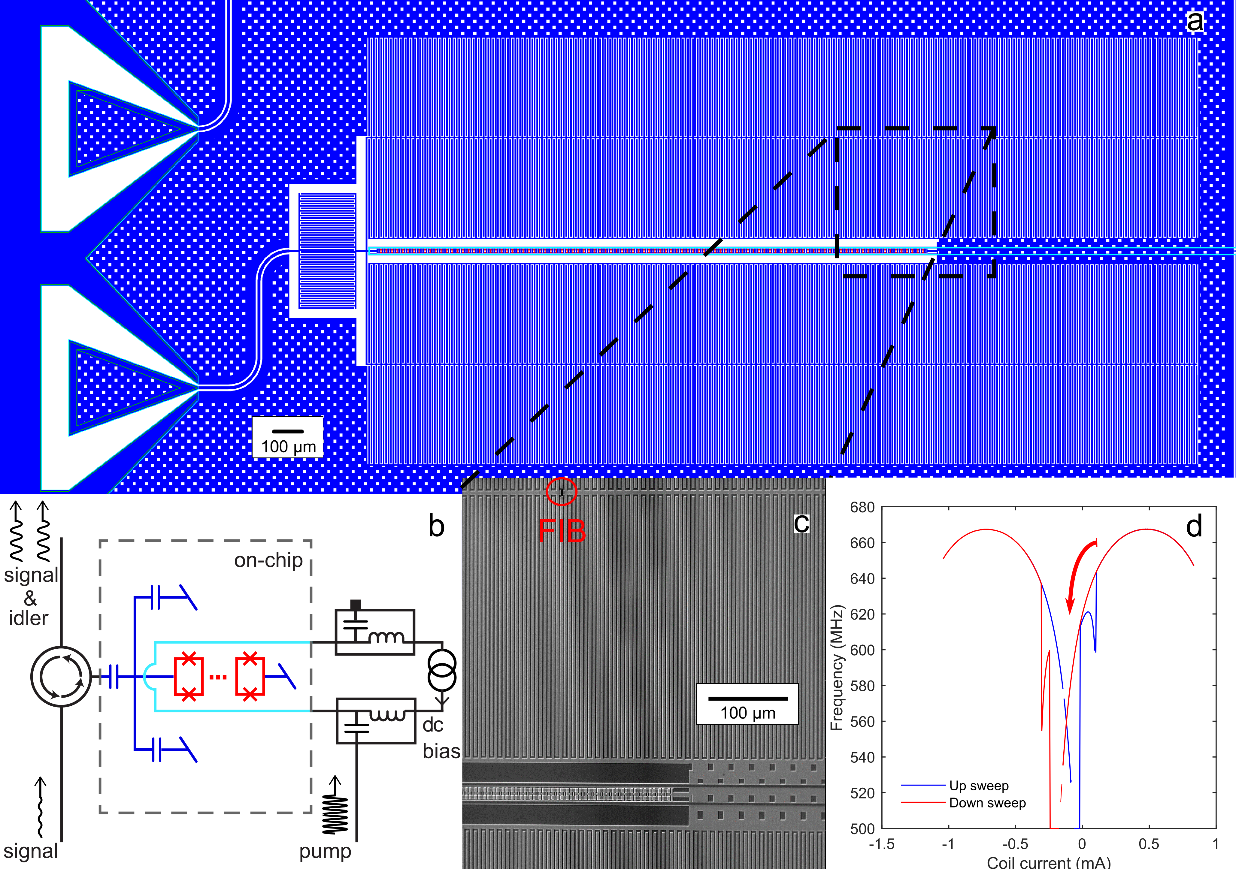
Two nominally identical devices A and B were prepared with the maximal resonance frequency targeted on 650 MHz, in order to make flux pumping feasible at the operating frequency of 600 MHz. The chip containing the JPA is placed on a holder and inside an aluminum-Amumetal 4K magnetic shield both of which are thermalized to the mixing stage of a dry dilution refrigerator. Prior to pumping, an initial characterization of the device takes place. It comprises the study of the small-signal response with a vector network analyzer (VNA) while tuning the resonance frequency with a magnetic flux, generated by a dc current applied to the FBL. A fit to the recorded reflection coefficient of the JPA allows us to determine the resonance frequency. Device A shows excellent reproducible tuneability between 520 MHz and 667 MHz [Fig. 1(d)] from which can be concluded that the SQUID array has a relatively homogeneous magnetic flux bias. Only a slight hysteresis occurs below 640 MHz probably in part because of the geometric inductances [41]. In contrast, the previous generation amplifier had very irregular frequency response and only two viable operating points [22]. There are several factors that could play a role in the observed improvement. First, a ground plane with flux-trapping holes [42] has been added to the device layout. Second, we have increased the size of the SQUID loops by 65 % to so that less dc current is needed in the FBL. Finally, we have paid special attention to using non-magnetic materials in close proximity to the JPA chip.
3 Gain and noise in the non-degenerate mode
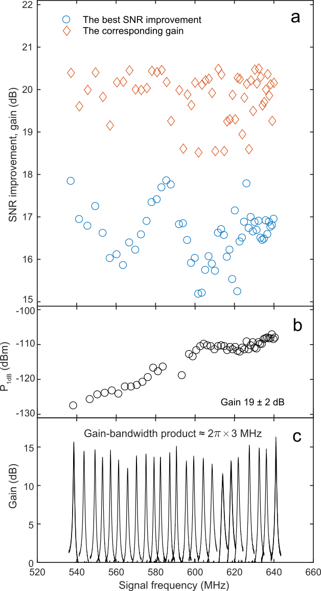
The JPA operating points defined by the triplet of the dc bias current, the associated flux pump frequency, and pump power are optimized and characterized by an automated procedure described in the Supplement. To study the gain and signal-to-noise ratio (SNR), we apply a weak probe tone at an offset of -10 kHz from the halved pump frequency where the JPA gain is maximal. The probe power is set to -146 dBm (-136 dBm) at frequencies below (above) 580 MHz, to adjust accordingly to the dynamic range. In the data of Fig. 2(a), the SNR is optimized at each static-flux operating point, while constraining the maximum gain to 20.5 dB. A gain of 18.5–20.5 dB is attained and the SNR improves by 15–18 dB, as compared to the unity-gain reference where the noise floor is set by the HEMT post-amplifier. The independently measured noise added by the HEMT is 10–13 K. The saturation of the JPA is investigated at the discovered operating points by varying the probe power [Fig. 2(b)] and it is found that the lower limit of -120 dBm, required for calorimeter readout, is easily surpassed by about 10 dB at 600 MHz. After increasing the pump frequency slightly to lower the gain to 15 dB, a gain-bandwidth product of MHz is measured [Fig. 2(c)]. It is sufficient for the detection of the thermal transients of the nano-calorimeter.
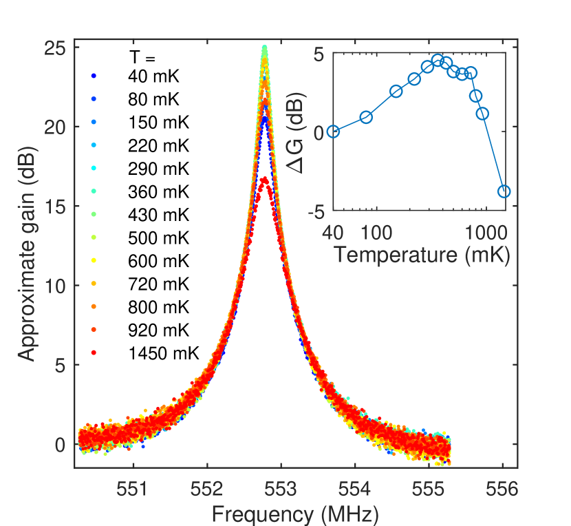
We investigate the potential range of the operating temperatures of Device A by setting a gain of 20 dB and measuring the JPA response with the VNA while heating the system. The frequency and power of the flux pump are kept at the fixed values. We attribute changes in the gain to the temperature dependence of the JPA resonance frequency. Raising the temperature from 40 mK to 80 mK (400 mK) increases the gain by 1 dB (5 dB). The gain stays above 20 dB below 1.0 K, and even at 1.5 K there is still a significant 16 dB of gain. The equivalent shift of the JPA resonance is 200 kHz, or 0.04 %. We note that these observations result from an interplay of several temperature-dependent quantities such as the permittivity of the Al2O3 coating of the JPA, the junction critical current, and the kinetic inductance of niobium [43].
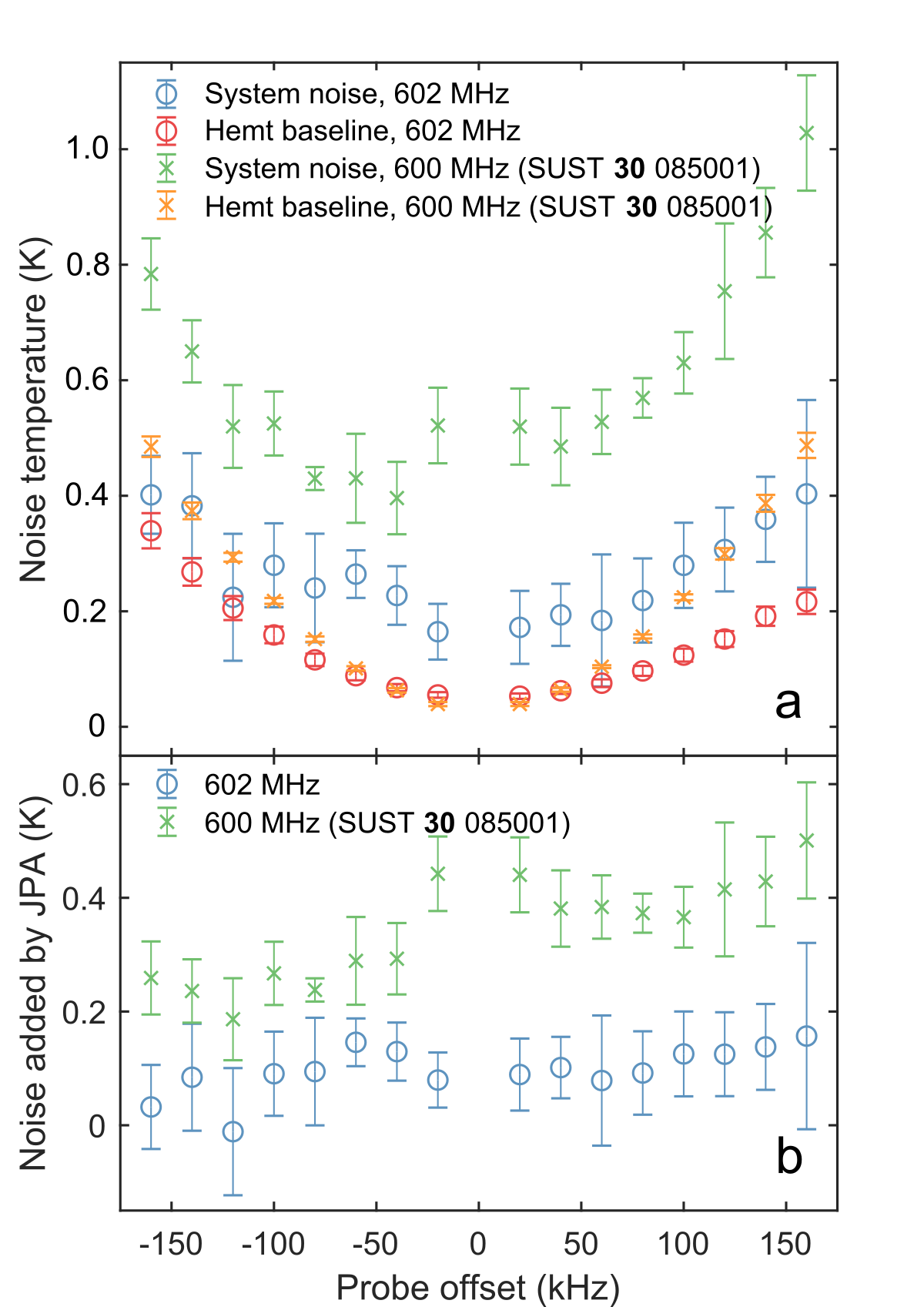
To better estimate the noise added by the JPA, the system noise temperature is determined with the Y-factor method [44]. Essentially, the power spectral density at the output of the JPA is surveyed with a spectrum analyzer while the JPA is subject to an impedance-matched resistive noise source with a controlled temperature. The source temperature is varied between 59 mK and 852 mK independently of the JPA temperature that is held constant at 30 mK with closed-loop control. The measurements are carried out with the Device B and the full setup is shown in the Supplement. The system noise temperature, referenced to the JPA input, takes its minimum value of 165 mK close to the halved pump frequency [Fig. 4(a)]. Since the noise added by the JPA is reasonably independent of the offset [Fig. 4(b)], we may take the average with the inverted variances as weights. This yields a noise estimate of 105 mK 9 mK. Making the comparison to Ref. 22, we note that the added noise has approximately halved. Also notable is that the noise is no longer at an elevated level at frequencies close to the gain maximum, which may be because the rf pump tone has been moved away from it to the double frequency.
4 Degenerate gain
In a dispersive sensor, such as the nano-calorimeters of Ref. 24, it is possible to choose the excitation and readout in such a way that the rf carrier and the information-carrying signal are in different quadratures. In this situation, it is possible to utilize squeezing to de-amplify the carrier and to amplify the signal. This may be used to effectively increase the dynamic range of the later stages of the readout. Ideally, the amplification does not add any noise if a JPA is used to perform the squeezing.
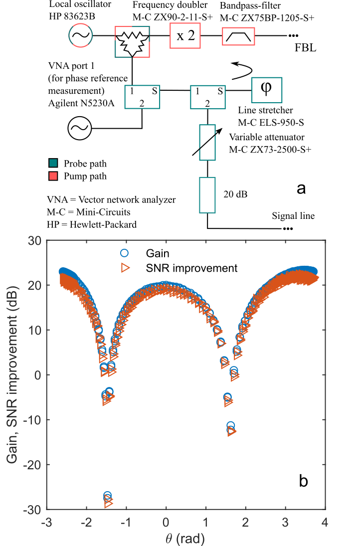
To observe squeezing in the degenerate mode of the JPA, where the pump is exactly at twice the probe frequency, a brief experiment is carried out with the Device B. Using a single rf source, the pump is synthesized with a frequency doubler and the relative phase of the probe is controlled as shown in Fig. 5(a). The JPA gain as a function of is -periodic as expected, and amplification and de-amplification alternate. The JPA is thus capable of squeezing [45]. However, here we do not attempt a proper investigation of the quadratures to determine how much vacuum squeezing is attainable.
5 Conclusion
We have overcome all the major issues discovered with the previous-generation JPA [22], and we have attained robust performance over a wide frequency range without sacrificing bandwidth, gain, or dynamic range. Additionally, we have minimized the amount of TLS-hosting dielectrics and their participation ratio with the SWAPS [32] fabrication process. This renders the JPA relatively insensitive to temperature, facilitating its use at variable mK-temperatures as only minor corrections to the JPA operating parameters are needed. Furthermore, the JPA is now flux-pumped at twice the readout frequency of the nano-calorimeter, easing the filtering required to avoid back-action such as residual heating by the pump. As an important step towards sub-GHz sensor readout at a fidelity beyond the standard quantum limit [46], squeezing has been observed in the degenerate mode of the JPA.
The noise added by the JPA has decreased to 105 mK at 600 MHz. This can largely be attributed to better isolation from the HEMT post-amplifier by means of an additional circulator. However, the added noise remains at an elevated level with respect to the lower bound set by the input thermal noise at 30 mK, likely due to poorly thermalized attenuators [47] or a fundamental limit of the amplifier itself. The noise performance also remains inferior to that of a microstrip SQUID amplifier with a reported noise temperature of 48 mK at 612 MHz [44]. Yet, we have demonstrated a sub-GHz JPA that is well suited for integration into a nano-calorimetry [24] or -bolometry [26] apparatus and we will pursue the latter goal in a future experiment.
Acknowledgments
We thank Paula Holmlund for sample preparation, Harri Pohjonen for help with lithographic masks, and Mikko Kiviranta for operating the FIB. We acknowledge the fruitful discussions with Olli-Pentti Saira, Roope Kokkoniemi, Mikko Möttönen, and Jukka Pekola. This work was performed as part of the Academy of Finland Centre of Excellence program (projects 284594, 312059, 251748, and 284621). The work also received funding from Academy of Finland project QuMOS (project numbers 288907 and 287768), Future Makers Funding Program by Technology Industries of Finland Centennial Foundation and Jane and Aatos Erkko Foundation.
References
- [1] Bradley R, Clarke J, Kinion D, Rosenberg L J, van Bibber K, Matsuki S, Mück M and Sikivie P 2003 Reviews of Modern Physics 75 777
- [2] Asztalos S J, Carosi G, Hagmann C, Kinion D, van Bibber K, Hotz M, Rosenberg L J, Rybka G, Hoskins J, Hwang J, Sikivie P, Tanner D B, Bradley R and Clarke J 2010 Physical Review Letters 104 041301
- [3] Kenany S A, Anil M A, Backes K M, Brubaker B M, Cahn S B, Carosi G, Gurevich Y V, Kindel W F, Lamoreaux S K, Lehnert K W, Lewis S M, Malnou M, Palken D A, Rapidis N M, Root J R, Simanovskaia M, Shokair T M, Urdinaran I, van Bibber K A and Zhong L 2017 Nuclear Instruments and Methods in Physics Research Section A: Accelerators, Spectrometers, Detectors and Associated Equipment 854 11–24
- [4] Bergeal N, Schackert F, Metcalfe M, Vijay R, Manucharyan V E, Frunzio L, Prober D E, Schoelkopf R J, Girvin S M and Devoret M H 2010 Nature 465 64–68
- [5] Abdo B, Sliwa K, Shankar S, Hatridge M, Frunzio L, Schoelkopf R and Devoret M 2014 Physical Review Letters 112 167701
- [6] O’Brien K, Macklin C, Hover D, Schwartz M E, Bolkhovsky V, Zhang X, Oliver W D and Siddiqi I 2016 Towards quantum-noise limited multiplexed microwave readout of qubits 2016 IEEE MTT-S International Microwave Symposium (IMS) pp 1–3
- [7] Devoret M H and Schoelkopf R J 2013 Science 339 1169–1174
- [8] Calusine G, Melville A, Woods W, Das R, Stull C, Bolkhovsky V, Braje D, Hover D, Kim D K, Miloshi X, Rosenberg D, Sevi A, Yoder J L, Dauler E and Oliver W D 2018 Applied Physics Letters 112 062601
- [9] Clark J B, Lecocq F, Simmonds R W, Aumentado J and Teufel J D 2016 Nature Physics 12 683–687
- [10] Yurke B, Kaminsky P G, Miller R E, Whittaker E A, Smith A D, Silver A H and Simon R W 1988 Physical Review Letters 60 764–767
- [11] Castellanos-Beltran M A and Lehnert K W 2007 Applied Physics Letters 91 083509
- [12] Yamamoto T, Inomata K, Watanabe M, Matsuba K, Miyazaki T, Oliver W D, Nakamura Y and Tsai J S 2008 Applied Physics Letters 93 042510
- [13] Mutus J Y, White T C, Jeffrey E, Sank D, Barends R, Bochmann J, Chen Y, Chen Z, Chiaro B, Dunsworth A, Kelly J, Megrant A, Neill C, O’Malley P J J, Roushan P, Vainsencher A, Wenner J, Siddiqi I, Vijay R, Cleland A N and Martinis J M 2013 Applied Physics Letters 103 122602
- [14] Eichler C and Wallraff A 2014 EPJ Quantum Technology 1 2
- [15] Mutus J Y, White T C, Barends R, Chen Y, Chen Z, Chiaro B, Dunsworth A, Jeffrey E, Kelly J, Megrant A, Neill C, O’Malley P J J, Roushan P, Sank D, Vainsencher A, Wenner J, Sundqvist K M, Cleland A N and Martinis J M 2014 Applied Physics Letters 104 263513
- [16] Eichler C, Salathe Y, Mlynek J, Schmidt S and Wallraff A 2014 Physical Review Letters 113 110502
- [17] Vissers M R, Erickson R P, Ku H S, Vale L, Wu X, Hilton G C and Pappas D P 2016 Applied Physics Letters 108 012601
- [18] Mallet F, Castellanos-Beltran M A, Ku H S, Glancy S, Knill E, Irwin K D, Hilton G C, Vale L R and Lehnert K W 2011 Physical Review Letters 106 220502
- [19] Fedorov K G, Zhong L, Pogorzalek S, Eder P, Fischer M, Goetz J, Xie E, Wulschner F, Inomata K, Yamamoto T, Nakamura Y, Di Candia R, Las Heras U, Sanz M, Solano E, Menzel E P, Deppe F, Marx A and Gross R 2016 Physical Review Letters 117 020502
- [20] Bienfait A, Campagne-Ibarcq P, Kiilerich A, Zhou X, Probst S, Pla J, Schenkel T, Vion D, Esteve D, Morton J, Moelmer K and Bertet P 2017 Physical Review X 7 041011
- [21] Clerk A A, Devoret M H, Girvin S M, Marquardt F and Schoelkopf R J 2010 Reviews of Modern Physics 82 1155–1208
- [22] Vesterinen V, Saira O P, Räisänen I, Möttönen M, Grönberg L, Pekola J and Juha Hassel 2017 Superconductor Science and Technology 30 085001
- [23] Gasparinetti S, Viisanen K L, Saira O P, Faivre T, Arzeo M, Meschke M and Pekola J P 2015 Physical Review Applied 3 014007
- [24] Viisanen K L, Suomela S, Gasparinetti S, Saira O P, Ankerhold J and Pekola J P 2015 New Journal of Physics 17 055014
- [25] Govenius J, Lake R E, Tan K Y, Pietilä V, Julin J K, Maasilta I J, Virtanen P and Möttönen M 2014 Physical Review B 90 064505
- [26] Govenius J, Lake R E, Tan K Y and Möttönen M 2016 Physical Review Letters 117 030802
- [27] Karasik B S and Cantor R 2011 Applied Physics Letters 98 193503
- [28] Suzuki T, Khosropanah P, Hijmering R A, Ridder M, Schoemans M, Hoevers H and Gao J R 2014 IEEE Transactions on Terahertz Science and Technology 4 171–178
- [29] Penfold-Fitch Z V, Sfigakis F and Buitelaar M R 2017 Physical Review Applied 7 054017
- [30] O’Connell A D, Ansmann M, Bialczak R C, Hofheinz M, Katz N, Lucero E, McKenney C, Neeley M, Wang H, Weig E M, Cleland A N and Martinis J M 2008 Applied Physics Letters 92 112903
- [31] Pappas D P, Vissers M R, Wisbey D S, Kline J S and Gao J 2011 IEEE Transactions on Applied Superconductivity 21 871–874
- [32] Grönberg L, Kiviranta M, Vesterinen V, Lehtinen J, Simbierowicz S, Luomahaara J, Prunnila M and Hassel J 2017 Superconductor Science and Technology 30 125016
- [33] Kiviranta M, Brandel O, Grönberg L, Kunert J, Linzen S, Beev N, May T and Prunnila M 2016 IEEE Transactions on Applied Superconductivity 26 1–5
- [34] Lähteenmäki P, Paraoanu G S, Hassel J and Hakonen P J 2013 Proceedings of the National Academy of Sciences 110 4234–4238
- [35] Devoret M and Roy A 2016 Comptes Rendus Physique 17 740–755
- [36] Supplementary information URL Supplementary information available online at.
- [37] Sandberg M, Wilson C M, Persson F, Bauch T, Johansson G, Shumeiko V, Duty T and Delsing P 2008 Applied Physics Letters 92 203501
- [38] Krantz P, Reshitnyk Y, Wustmann W, Bylander J, Gustavsson S, Oliver W D, Duty T, Shumeiko V and Delsing P 2013 New Journal of Physics 15 105002
- [39] Svensson I M, Bengtsson A, Krantz P, Bylander J, Shumeiko V and Delsing P 2017 Physical Review B 96 174503
- [40] Zhou X, Schmitt V, Bertet P, Vion D, Wustmann W, Shumeiko V and Esteve D 2014 Physical Review B 89 214517
- [41] Pogorzalek S, Fedorov K G, Zhong L, Goetz J, Wulschner F, Fischer M, Eder P, Xie E, Inomata K, Yamamoto T, Nakamura Y, Marx A, Deppe F and Gross R 2017 Physical Review Applied 8 024012
- [42] Chiaro B, Megrant A, Dunsworth A, Chen Z, Barends R, Campbell B, Chen Y, Fowler A, Hoi I C, Jeffrey E, Kelly J, Mutus J, Neill C, O’Malley P J J, Quintana C, Roushan P, Sank D, Vainsencher A, Wenner J, White T C and Martinis J M 2016 Superconductor Science and Technology 29 104006
- [43] Annunziata A J, Santavicca D F, Frunzio L, Catelani G, Rooks M J, Frydman A and Prober D E 2010 Nanotechnology 21 445202
- [44] Kinion D and Clarke J 2011 Applied Physics Letters 98 202503
- [45] Zhong L, Menzel E P, Di Candia R, Eder P, Ihmig M, Baust A, Haeberlein M, Hoffmann E, Inomata K, Yamamoto T, Nakamura Y, Solano E, Deppe F, Marx A and Gross R 2013 New Journal of Physics 15 125013
- [46] Caves C M 1982 Physical Review D 26 1817–1839
- [47] Yeh J H, LeFebvre J, Premaratne S, Wellstood F C and Palmer B S 2017 Journal of Applied Physics 121 224501