Coherent Transport in Y-Junction Graphene Waveguide
Abstract
We performed a series of theoretical transport studies on Y-branch electron waveguides which are embedded in mid-size armchair graphene nanoribbons (AGNRs). Non-equilibrium Green’s function (NEGF) with different approximations of tight-binding (TB) Hamiltonian has been employed. Using the first nearest hopping approximation, we observed very pronounced conductance quantization, the structure of which depends on geometrical design and shows a spacing of , indicating the existence of valley degree of freedom. Moreover, by incorporating the third nearest approximation, we observed seminal plateaus deviated from multiples of conductance, suggesting the lift of valley degeneracy. Finally, Quasi-one dimensional band structure calculations have been performed to study the availability of energy channels and the role of the major geometrical parameters on the transport.
I Introduction
In the past decade, many theoretical studies have been proposed to realize the coherent transports in ideal straight graphene nanoribbons (GNRs) peres2006conductance ; gunlycke2007semiconducting ; dubois2009electronic . However, the quantization of conductance, which is the hallmark of coherent transport in 1D systems, is usually missing in plasma etched GNRs due to the edge disorders that produce strong scattering lin2008electrical ; lian2010quantum ; tombros2011quantized ; wurm2009interfaces ; mucciolo2009conductance ; lherbier2008transport ; orlof2013effect ; baldwin2016effect . Perhaps this major problem has hindered graphene’s application in sophisticated nanoelectronics (such as spin qubit devices) despite its excellent conductivity recher2010quantum ; chiu2017single ; deng2015charge . An alternative approach to replicate a GNR is to introduce a well-like electrostatic confinement in graphene, also known as graphene waveguide (GWG), in which the crystal structure between side-barriers and quantum well remains intact tudorovskiy2007spatially. As a result of the electrostatic confinement, there are discrete bound states spatially extended along the graphene waveguide. Quantized conductance in 1D systems had long been realized in modulation-doped GaAs/AlGaAs heterostructures where a pair of negatively biased split gates deplete the two-dimensional electron gas (2DEG) underneath and define a 1D channel yacoby1996nonuniversal . The situation for graphene-based waveguide is expected to be different from the aforementioned 2DEG case, since the existence of transparent Klein tunneling could play an essential role and limit the ability of GWG for efficient guiding katsnelson2006chiral ; allain2011klein . Interestingly, some theoretical approaches using Dirac equation have in fact suggested that carriers in an infinite GWG is behaving in many respects like the optical waves in an optical-fiber (that is, they display optics-like features) beenakker2009quantum ; hartmann2014quasi ; dragoman2010polarization . However, it is worth noting that the theory of Klein tunneling on graphene is based on first-nearest approximation (Dirac Hamiltonian) and the assumption of the plane wave solution. A precise but relatively expensive numerical method incorporating few more nearest-neighbors hopping terms, called the Non-equilibrium Green’s function (NEGF), can be employed to have a better understanding about the feasibility of the perfect transmission in GWG datta2005quantum . Such a numerical simulation can also provide more details on the conditions that lead to a coherent or imperfect transmission. Current experimental evidences are not, however, in favor of the total reflection of carriers from borders of a GWG as Snell’s law would hold in the optical-fiber. In particular, the reported guiding efficiencies do not exceed 80% and differ among different 1D energy modes williams2011gate ; rickhaus2015guiding . In our previous calculations, we have shown that a single GWG (S-GWG) can possess the characteristics of a coherent transport and the desirable insensitivity to the bending degree mosallanejad2018perfectly. A further interesting question for us is whether a coherent splitting of current can be realized in GWGs. In this letter, we provide theoretical evidences to show that it is possible to coherently split the incoming current into two paths in a Y-junction graphene waveguide (YJ-GWG). Our results show the prospect of using YJ-GWGs as a splitter in all graphene-based electronic devices that require robust phase coherence, and therefore can be potentially used as an interconnect in spintronic devices. A YJ-GWG can be made by applying a positive potential to an external Y-branch metal gate which is isolated from graphene flake and consequently it induces a Y-shape potential well in graphene. Mathematically, a reasonable estimation of 2D on-site potential (a cut-plan of 3D electrostatic potential) suitable for modeling of YJ-GWG could be produce by making use of two bended S-GWG with an overlapping area as it explained in appendix A. The influence of geometrical design on the coherent transport is discussed in detail in the main text. Furthermore, Quasi-one dimensional bandstructure calculations have been performed to study the energy channels that could contribute to the transport.
II Methods
II.1 Device structure
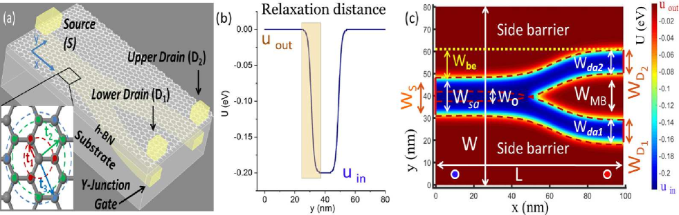
The schematic of our proposed structure is shown in Fig. 1(a), which consists of a finite mid-size AGNR with an integrated Y-junction gate underneath it. Hexagonal boron nitride (h-BN), an atomically thin insulating material, is used simultaneously as a gate dielectric and a secondary substrate to improve the mobility of graphene zomer2011transfer ; zhang2017electrotunable . A YJ-GWG can be defined by applying a positive potential to the underlying gate and consequently induces a Y-shape potential well in the AGNR. Single potential well on the left side thus splits into two wells, one goes upward and the other goes downward beyond the intersection, i.e., the system has in total three terminals. The source and drain terminals are located exactly above the respective branches of the Y-junction, which is denoted by S, D1 and D2, respectively. In general, a self-consistent solution of Schrödinger equation (in the form of Green’s function formalism) coupling to a Poissons equation should be used to simulate the electrostatics of the device and the transmission through terminals, simultaneously akhavan2012phonon ; banadaki2015investigation . However, this model can not be realized here due to the numerical complexity arising from the large number of atoms in our system. To compensate the lack of full self-consistent solution, a representative potential well with a cross section as illustrated in Fig. 1(b) has been used to define YJ-GWG in our AGNR. In a real device, the relaxation distance between the top and bottom of the potential well depends on the thickness and dielectric constant of the substrates. The thinner the insulators (e.g., hBN) are, the sharper the potential well will be. The on-site potential of carbon atoms in a real 2D device is shown in Fig. 1(c), in which the YJ-GWG formed by the combination of two S-shape waveguides, is indicated by dashed lines. The 2D device (AGNR) consists of two main parts. First, a fairly large intrinsic channel with width W and Length L, while represent the width of three arms of YJ-GWG, i.e., source arm, lower drain arm and upper drain arm, respectively. In the standard convention, AGNRs are labeled as NA-AGNR where NA is the number of dimer lines defined by N, W is the width of AGNR and nm is the carbon-carbon bond length. The second part of our device is the contacts (source and drains) which are also made of carbon and are in fact extensions from the scattering area, as illustrated by vertical red lines in Fig. 1(c). The widths of all terminals are tailored to be matched with waveguide arms, i.e., WS = Wsa, W = W. In all numerical examples, we have chosen metallic type of supercells (or (3m+2) family of AGNRs) for all terminals to artificially replicate a real metal contact. The reason to use these GNRs instead of metal is to provide good ohmic contacts owing to the workfunction match. The length of scattering area (L) is related to the number of supercells (NS) via N. WO represents the amount of overlap between the two flat ends of S-shape GWGs, and is the width of middle barrier between the two s. Wsa and WMB are related to WO via Wsa=W+W-WO and WO/2+WMB/2=Wbe, where Wbe can be viewed as the amount of bending.
II.2 Numerical model
The orbital wavefunction of Carbon is used to construct TB-Hamiltonian for channels and terminals,
| (1) |
where and are the creation and annihilation operators at -th atomic site, respectively. The symbol denotes a pair of atomic sites and the relevant hopping parameters are real energy values.
| Set | |||||||
|---|---|---|---|---|---|---|---|
| 1NN | 0 | -2.78 | 0 | 0 | 0 | 0 | 0 |
| 3NNI | -0.45 | -2.78 | -0.15 | -0.095 | 0.117 | 0.004 | 0.002 |
| 3NNII | -0.187 | -2.756 | -0.071 | -0.38 | 0.093 | 0.079 | 0.070 |
We have assumed the first nearest and two other third nearest approximations denoted by 1NN and 3NNI,II in different cases to comprehend the impact of them on transport. The relevant TB parameters for 1NN and 3NNI,II are shown in Table 1. In particular, the new TB parameters, 3NNII, obtained from density functional theory (DFT), has shown excellent agreement with the predictions of the DFT even in the high-energy region reich2002tight ; kundu2011tight ; tran2017third . The effect of the potential well on the transmission is directly considered through the on-site potential energy on the Hamiltonian, i.e., in Eq. (1). The assigned potential map for the Y-junction is shown in Fig. 1(c), in which the value of in the bottom of Y-shape potential well is , and that in the barrier regions has a fix value . Similarly, on-site potential of source and drains terminals in their Hamiltonian are noted as and , which are used to represent an applied bias voltage. The effect of edge roughness in the GNR is not included in our calculation gunlycke2008tight . Because the edge roughness can be far from the potential-defined Y-junction and if a very wide GNR is considered, their effect on the transport in YJ-GWG can be neglected. The effect of electron-phonon interactions is not included in this work either, due to the weak electron-phonon interactions in graphene borysenko2010first . Using the Landauer-Bütticker formalism datta2005quantum , the conductance between the source and drains in low temperature can be expressed as:
| (2) |
where is the quanta of conductance that includes the spin degree of freedom, are the source and drains broadening matrices, which couple the left and right terminals to the central scattering region in YJ-GWG. The retarded Green’s function is defined as and , where S is the overlap matrix and is in the form of the first part in equation (1). The open boundary condition of terminals is added via , where and are self-energies of the semi-infinite terminals on the source and drains. The transport simulation of YJ-GWG is carried out by our ballistic code in which we have used the direct recursive algorithm to calculate conductance of a system with few hundred thousand of atoms lewenkopf2013recursive ; thor2014recursive . This Memory-friendly approach allows us to perform partial inversion of a gigantic matrix, which is a necessary mathematical operation to calculate the Green’s function in real space.
III Results and Discussion
III.1 Tunning
Y-junction gate voltage is used to control the depth of quantum well and consequently provide deep-enough confined energy channels. By this manner, the bottom of on-site potential, i.e., , can be parametrically tuned to achieve a coherent transport in the device. Moreover, our previous work has demonstrated that on-site potential of terminals is an equally vital parameter to achieve the coherent transport in a two-terminal graphene waveguide mosallanejad2017perfectly .
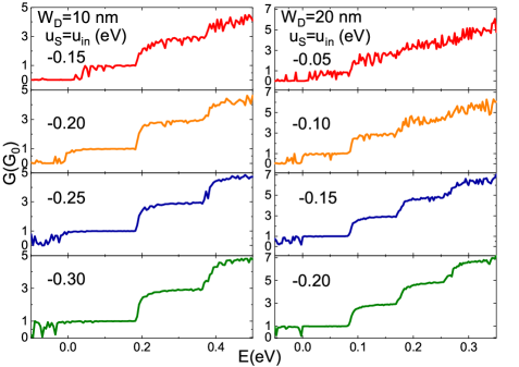
It has been concluded that the quantization of conductance occurs if the following conditions were met: (i) the terminals have similar width of the waveguide, (ii) the source has a fix on-site potential almost equal to that in the bottom of waveguide (i.e., ), (iii) on-site potential at the drain is kept zero, which is equal to .To quantitatively determine an appropriate range of as a primary study, a few two-terminal transport studies were performed for two curved S-GWGs with waveguide widths () of 10 nm and 20 nm. The on-site potential profile of such systems is similar to that in Fig. 1(c) but the negative potential well (blue color) is placed only within one arm. For each sample, has been swept over a range of values under the conditions of and . Conductances on all upper panels of Fig. 2 (in both sizes), show that shallower wells (small negative ) are incapable to produce smooth plateaus (note that we have employed 1NN approximation in these calculations). Once the well gets deeper, more well-defined smooth plateaus start to form. Furthermore, narrower waveguide (10 nm) needs deeper potential well to produce smooth plateaus. Thus, it is essential to have a deep-enough well via applying appropriate gate voltages. Independent comparison between the right and left panels of Fig. 2 shows that number of plateaus within the same energy range is somehow, insensitive to the depth of potential well but rather dependent on the width of the waveguide. This fact indicates that the width of waveguide determines the conductance profile if the potential is deep enough. Since provide smooth plateaus for the 10 nm wide waveguide, hereafter, we will use these quantitative values in the transport study of YJ-GWG in the next section.
III.2 Transport study in YJ-GWG
Start with a given drain width nm, four samples with different and are created and the conductances of both paths in each sample are evaluated. The dimension of the system is and paths have symmetry around . Center of bending is located in the middle of x-direction at . Calculated results are shown in Fig. 3(a)-(d).
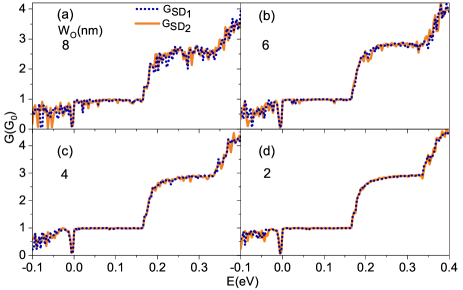
has been selected as the first control parameter to study the effect of overlap, partially because other parameters, such as , (which represents the amount of bending) has shown very less influences on the conductance of a S-GWG. Lower panels of Fig. 3, (c) and (d), with smooth and identical plateaus for both paths, demonstrate that it is possible to transport carriers coherently in both paths of a YJ-GWG provided that the parameter is small enough. By comparing all panels in Fig. 3, one can find a noticeable smooth conductance which was achieved when the width of the source arm increases (because of Wsa=W+W-WO). In addition, another type of YJ-GWG has been constructed based on a kink-shape bending to study the effect of sharp bending. Variation of waveguide width occurs around the sharp bending, indicated by arrows in the Fig. 4(a), within which the width of waveguide differs from in comparison with the fully-smooth S-shape bending shown by dashed lines in the Fig. 4(a).
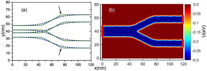
S-shape bending ensures that the width of both paths remains unchanged after the splitting point. Since the energy channels are highly sensitive to the width of single-waveguide, width variations in sharp bendings are expected to induce extra scatterings that affect the conductance quality. Fig. 5(a)-(d) show the calculated conductances of the kink-shape YJ-GWG with different . Fig. 5 supports our argument and indeed shows more noisy conductances, especially in the second plateau.
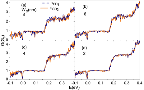
Note that except for the shape of the waveguide, all other parameters used in Fig. 5 are similar to those used in Fig. 3 (note that the third nearest approximation, denoted by 3NNI has been employed for both cases).
We further have investigated the geometrical effect on transport by enlarging the whole device by a scale factor of 1.5 but keeping the Y-shape structure unchanged. Accordingly, scattering area of , arm’s width of nm, nm and have been taken into the account.
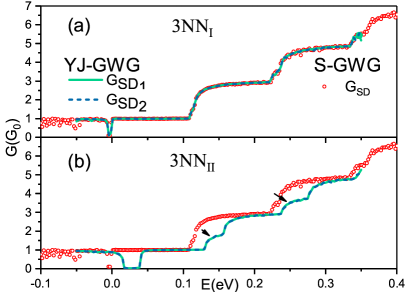
Conductances of two paths have been shown by dashed and solid lines in Fig. 6(a). Comparison of conductances between Fig. 3(d) and Fig. 6(a) implies that scaling has minor effect on general characterizations of the YJ-GWG. In Fig. 6(a), the third nearest approximation, denoted by 3NNI has been used whereas 3NNII is employed to calculate conductances of YJ-GWG in Fig. 6(b). One can conclude that the new TB parameter set has lifted the valley degeneracy and produced multiple sub-plateaus illustrated by arrows in Fig. 6(b). Careful observers may notice seminal plateaus on the results calculated by 3NNI as well [Fig. 6(a)]. Red-hallow circles show the conductance of the relevant two-terminal S-GWG (only one arm) with similar parameters and 3NNI energy set as a reference. Comparison between red-hallow circles, dashed and solid lines in Fig. 6(a) tells us, the conductances of YJ-GWG almost follow the conductance of a relevant S-GWG. In Fig. 6(b), it also shows 3NNII approximation results in a shift of conductances toward the positive side of energy axis.
III.3 Bandstructure Remarks
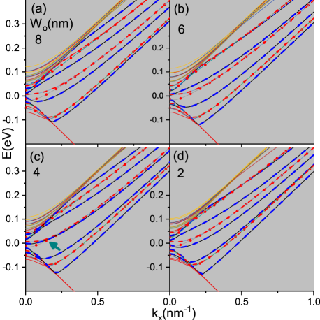
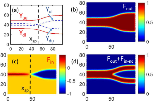
In order to obtain more insight on our results, we have calculated quasi-one dimensional bandstructure for two supercells, one at the left end of AGNR, e.g., x = 10 nm (with single-well) and the other at the right end, e.g., x = 90 nm (with double well). The positions of those supercells are specified by blue and red dots in Fig. 1(b). The calculated bands, which contain sixteen conduction bands and one valance band in the positive momentum space, are shown in Fig. 7(a)-(d). Thus, it is possible to track the movement of subbands in energy space at different . A single-well possess two-fold degenerate bands which are highlighted by blue dashed and black narrow solid lines whereas double-well results in four-fold degenerate bands which are denoted by a red dashed, a red dotted line and two (multi-color) narrow solid lines together. Subbands belong to the barriers, which are located above the highlighted bands, are shown by multi-color narrow solid lines. All panels in Fig. 7 show that change in (or ) does not shift the energy bands of double-well substantially, whereas similar change of shift down the bands of a single well. Note that decrease in leads to a similar increase in , because , where is fixed. Thus adjusting is a practical method to match energy channels at the two ends of scattering area. This diagram also explains why the smooth conductance occurs when nm at Fig 3(c). We can see the two types of energy bands, shown by a tip of arrow, cross each other around the Dirac point at Fig. 7(c). The calculated band structures indicate that lower energy bands with do not participate in the quantized transport.
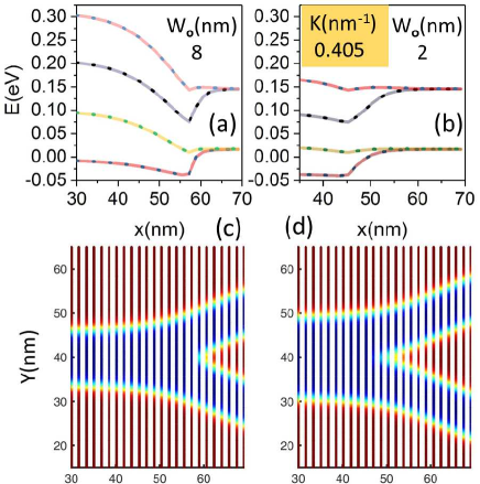
It is possible to explain a physical reason of our theoretical observation from the energy point of view. It is widely accepted that scattering happens as a result of mismatch between energy levels along the transport direction. For example, impurity levels might destructively couple to transport channels and smear the quantization of conductance. Here in YJ-GWG, one can expect minimum scattering if energy channels merge to each other with minimum misalignment around Y-junction. Therefore, we have further investigated our study by extracting spatial-resolved energy spectrum, i.e. waveguide energy channels, of few super-cells along x and around the splitting point, as plotted in Fig. 8(a) and (b) for a fix momentum kx= 0.405 (). Relative on-site potential used for the calculation in Fig.8 (a) and (b) are plotted in Fig. 8(c) and (d), respectively. One can see that two-fold degenerate energy bands (second and fourth levels) on the left side of Y-junction merge to four-fold degenerate bands on the right side. The amount of energy level variations are much less for the case of Wo = 2nm as compare to Wo = 8nm. Note that, one can expect similar merging trends for other higher momentums, since the E-kx relationship is linear for other larger values of momentum. From band structure studies, Fig. 8(a) and (b), one can see obviously that the energy spacing between first and second four-fold bands, spatially available on the right side of device, is about 150 meV which is noticeably large and consistent with the width of first flat plateaus on the energy range at Fig. 3.
III.4 Discussion
After the realization of quantized conductance on quantum point contact (QPC), Y-junction structures on modulation-doped heterostructures have been proposed and fabricatedvan1988quantized ; maao1994quantum ; shorubalko2003tunable . Different terminologies have been used to address similar devices such as Y-branch switch (YBS) and three-terminal ballistic junction (TBJ). A gate defined YBS hardly works in ballistic regime or in another world the quantization of conductance is rarely reported as a prominent characteristic of deviceshorubalko2003tunable . Whereas, peaks on the derivative of conductance on wet-etched version of YBS demonstrate the presence of quantizationworschech2005nonlinear ; jones2005quantum . This is probably because subband-spacings in a gate defined 1D quantum wire are limited to the order of a few meV while larger energy spacing in a wet-etched GaAs/AlGaAs quantum wires, typically on the order of a few tens of meV, have been reported. Note that, the conductance of wet-etched YBS does not exhibits flat plateaus and an exact identical I-V characteristic have not been reported. On the other hand, carbon nanotube Y-junction (CNT-YJ), T-shaped GNR (T-GNR) and few Cross-shape GNR (C-GNR) have been widely studied theoreticallyandriotis2001rectification ; andriotis2002transport . The conductance of CNT-YJ shows oscillatory behavior in theoretical studies which merely depends on geometry of system. To the best our knowledge quantization of conductance does not report on chemically synthesized Y-junctions nanotube and both T-GNR and C-GNR do not exhibit quantization of conductance as wellouyang2009transport ; bandaru2005novel ; brandimarte2017tunable . A prominent benefit of the proposed structure is the flat plateaus on conductance of a smooth YJ-GWG, Fig. 3(d), which is not reported in other possible carbon base splitters so far. The optimization of the width of incoming path on a smooth-bended YJ-GWG can be considered as a viable method to achieve the goal of coherent splitting. YJ-GWG can be a gateway for the realization of possible carbon-base electron interference devices, as well as interconnect in graphene-based spintronic devices.
IV Conclusions
In conclusion, we have exploited the possibility of coherent transport through a Y-junction graphene waveguide. Results show that if the incoming path of YJ-GWG is wide enough, the conductances of both paths are identical to the single graphene waveguide. It has been shown that smoothly bended GWG provide much smoother plateaus on the conductance. The primitive YJ-GWG enlarged by a scale factor of 1.5 and the results of transport study show that the quantization of conductance is well preserved in a larger device. In addition, we have shown that the influence of different TB energy sets on the calculation of conductance. A quasi-one dimensional bandstructure calculation was also performed to explain our observations.
Acknowledgments
This work was supported by the National Key Research and Development Program of China (Grant No. 2016YFA0301700), the National Natural Science Foundation of China (Grants No. 11625419),and the Anhui Initiative in Quantum Information Technologies (Grants No. AHY080000). We should also thank Chinese Academy of Sciences and The World Academy of Science for the advancement of science in developing countries.
Appendix A Y-junction on-site potential
We have accomplished the following steps to build a 2D on-site potential of YJ-GWG including relaxation distance where values of potential energy inside and outside of Y-junction are uin and uout.
Step 1 ; Calculate functions, and , to define upper and lower edge lines of the downward bended S-GWG (i.e., downward lines in Fig. 9(a)),
| (3) | |||||
| (4) |
and and to define lower and upper borders of the upward bended S-GWG (i.e., upward lines in Fig. 9(a))
| (5) | |||||
| (6) |
where is the Fermi function which is employed only to produce smooth variation along the x direction. sets the center of YJ-GWG on the y direction, is the inflection point of bended lines on the x direction and defines the sharpness of bending in this direction. A bigger provides a smooth and adiabatic variation along the x direction. Throughout all studies with smooth bending, the value of is .
Step 2 ; Once again Fermi function is employed to establish another smooth step-like functions in y-direction which their inflection points define by making use of previously determined border functions i.e., as follow;
| (7) |
where the index refers to one of ul, uu, du and dl. We should remind that and are x and y coordinations of i-th atom. determines relaxation distance () on transverse direction. One can easily conclude if and approximate upper and lower limits of Fbo. We have considered 4 nm on all of our structures.
Step 3 ; The subtraction provide a function which smoothly varies from zero on both side-barrier areas to the one on the middle of outer lines i.e., and , red solid lines in Fig. 9(a). is plotted in Fig. 9(b). Utilization of Fermi function on step 2 ensures that the full width of half maximum (FWHM) of waveguide is equal to the distance between border lines because the value of s are 1/2 on inflection points. Note that and , dashed lines in Fig. 9(a), cross each other on the splitting point (). At the same time, for the subtraction provide us a function which smoothly varies from negative one on the middle-barrier (MB) region, the areas that is trapped between inner border lines (du and ul), to zero on side-barrier areas, see Fig. 9(c). gives a positive value for overlapping area which we cancel it by signing the positive values to zero and call the new function .
Step 4 ; delivers a Y-splitter function with
zero value on all (three) barriers and positive one within the Y-branch, see Fig. 9(d).
Step 5 ; Finally, proper estimation of on-site potential of YJ-GWG is given by adding potential amplitudes as follow
| (8) |
One can build a kink-shape on-site potential with similar process except kink-shape border lines must be taken into account instead of smooth lines in step 1.
References
- (1) N. Peres, A. C. Neto, and F. Guinea, Physical Review B 73, 195411 (2006).
- (2) D. Gunlycke, D. Areshkin, and C. White, Applied Physics Letters 90, 142104 (2007).
- (3) S.-M. Dubois, Z. Zanolli, X. Declerck, and J.-C. Charlier, The European Physical Journal B 72, 1 (2009).
- (4) Y.-M. Lin, V. Perebeinos, Z. Chen, and P. Avouris, Physical Review B 78, 161409 (2008).
- (5) C. Lian, K. Tahy, T. Fang, G. Li, H. G. Xing, and D. Jena, Applied Physics Letters 96,103109 (2010).
- (6) N. Tombros, A. Veligura, J. Junesch, M. H. Guimar aes, I. J. Vera-Marun, H. T. Jonkman,and B. J. Van Wees, Nature Physics 7, 697 (2011).
- (7) J. Wurm, M. Wimmer, I. Adagideli, K. Richter, and H. U. Baranger, New Journal of Physics 11, 095022 (2009).
- (8) E. R. Mucciolo, A. C. Neto, and C. H. Lewenkopf, Physical Review B 79, 075407 (2009).
- (9) A. Lherbier, B. Biel, Y.-M. Niquet, and S. Roche, Physical review letters 100, 036803 (2008).
- (10) A. Orlof, J. Ruseckas, and I. V. Zozoulenko, Physical Review B 88, 125409 (2013).
- (11) J. Baldwin and Y. Hancock, Physical Review B 94, 165126 (2016).
- (12) P. Recher and B. Trauzettel, Nanotechnology 21, 302001 (2010).
- (13) K.-L. Chiu and Y. Xu, Physics Reports 669, 1 (2017).
- (14) G.-W. Deng, D. Wei, J. Johansson, M.-L. Zhang, S.-X. Li, H.-O. Li, G. Cao, M. Xiao, T. Tu, G.-C. Guo, et al., Physical review letters 115, 126804 (2015).
- (15) T. Y. Tudorovskiy and A. Chaplik, JETP letters 84, 619 (2007).
- (16) A. Yacoby, H. Stormer, N. S. Wingreen, L. Pfeiffer, K. Baldwin, and K. West, Physical review letters 77, 4612 (1996).
- (17) M. Katsnelson, K. Novoselov, and A. Geim, Nature physics 2, 620 (2006).
- (18) P. E. Allain and J.-N. Fuchs, The European Physical Journal B 83, 301 (2011).
- (19) C. Beenakker, R. Sepkhanov, A. Akhmerov, and J. Tworzyd lo, Physical review letters 102, 146804 (2009).
- (20) R. R. Hartmann and M. Portnoi, Physical Review A 89, 012101 (2014).
- (21) D. Dragoman, JOSA B 27, 1325 (2010).
- (22) S. Datta, Quantum transport: atom to transistor (Cambridge university press, 2005).
- (23) J. Williams, T. Low, M. Lundstrom, and C. Marcus, Nature Nanotechnology 6, 222 (2011).
- (24) P. Rickhaus, M.-H. Liu, P. Makk, R. Maurand, S. Hess, S. Zihlmann, M. Weiss, K. Richter, and C. Schonenberger, Nano letters 15, 5819 (2015).
- (25) V. Mosallanejad, K. Wang, Z. Qiao, and G. Guo, Journal of Physics: Condensed Matter 30, 325301 (2018).
- (26) P. Zomer, S. Dash, N. Tombros, and B. Van Wees, Applied Physics Letters 99, 232104 (2011).
- (27) Z.-Z. Zhang, X.-X. Song, G. Luo, G.-W. Deng, V. Mosallanejad, T. Taniguchi, K. Watanabe, H.-O. Li, G. Cao, G.-C. Guo, et al., Science advances 3, e1701699 (2017).
- (28) N. D. Akhavan, G. Jolley, G. A. Umana-Membreno, J. Antoszewski, and L. Faraone, Journal of Applied Physics 112, 094505 (2012).
- (29) Y. M. Banadaki and A. Srivastava, Solid-State Electronics 111, 80 (2015).
- (30) S. Reich, J. Maultzsch, C. Thomsen, and P. Ordejon, Physical Review B 66, 035412 (2002).
- (31) R. Kundu, Modern Physics Letters B 25, 163 (2011).
- (32) V.-T. Tran, J. Saint-Martin, P. Dollfus, and S. Volz, AIP Advances 7, 075212 (2017).
- (33) D. Gunlycke and C. White, Physical Review B 77, 115116 (2008).
- (34) K. M. Borysenko, J. T. Mullen, E. Barry, S. Paul, Y. G. Semenov, J. Zavada, M. B. Nardelli, and K. W. Kim, Physical Review B 81, 121412 (2010).
- (35) C. H. Lewenkopf and E. R. Mucciolo, Journal of Computational Electronics 12, 203 (2013).
- (36) G. Thorgilsson, G. Viktorsson, and S. Erlingsson, Journal of Computational Physics 261, 256 (2014).
- (37) B. Van Wees, H. Van Houten, C. Beenakker, J. G. Williamson, L. Kouwenhoven, D. Van der Marel and C. Foxon, Physical review letters 60, 848 (1988).
- (38) F. A. Maao,I. Zozulenko and E. H. Hauge, Physical Review B 50, 17320 (1994).
- (39) I. Shorubalko,H. Xu, P. Omling and L. Samuelson, Applied Physics Letters 83, 2369 (2003).
- (40) L. Worschech, D. Hartmann, S. Reitzenstein and A. Forchel, Journal of Physics: Condensed Matter 17, R775 (2005).
- (41) G. Jones, C. Yang, M. Yang and Y. Lyanda-Geller, Applied Physics Letters 86, 073117 (2005).
- (42) A. N. Andriotis, M. Menon, D. Srivastava and L. Chernozatonskii, Physical review letters 87, 066802 (2001).
- (43) A. N. Andriotis, M. Menon, D. Srivastava and L. Chernozatonskii, Physical Review B 65, 165416 (2002).
- (44) F. OuYang, J. Xiao, R. Guo, H. Zhang and H. Xu, Nanotechnology 20, 055202 (2009).
- (45) P. R. Bandaru, C. Daraio, S. Jin and A. Rao, Nature Material 4, 663 (2005).
- (46) P. Brandimarte, M. Engelund, N. Papior ,A. Garcia-Lekue, T. Frederiksen and D. Sánchez-Portal, The Journal of Chemical Physics 146, 092318 (2017).