Nanophotonic Pockels modulators on a silicon nitride platform
Abstract
Silicon nitride (SiN) is emerging as a competitive platform for CMOS-compatible integrated photonics. However, active devices such as modulators are scarce and still lack in performance. Ideally, such a modulator should have a high bandwidth, good modulation efficiency, low loss, and cover a wide wavelength range. Here, we demonstrate the first electro-optic modulators based on ferroelectric lead zirconate titanate (PZT) films on SiN, in both the O- and the C-band. Bias-free operation, bandwidths beyond 33 GHz and data rates of 40 Gbps are shown, as well as low propagation losses ( dB/cm). A 3.2 Vcm is measured. Simulations indicate that values below 2 Vcm are achievable. This approach offers a much-anticipated route towards high-performance phase modulators on SiN.
pacs:
42,78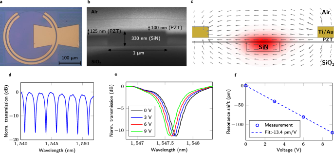
The exponential increase in data traffic requires high capacity optical links. A fast, compact, energy efficient, broadband optical modulator is a vital part of such a system. Modulators integrated with silicon (Si) or silicon nitride (SiN) platforms are especially promising, as they leverage CMOS fabrication techniques. This enables high yield, low-cost and scalable photonics, and a route towards co-integration with electronics Sun2015single . SiN-based integrated platforms offer some added advantages compared to silicon-on-insulator (SOI), such as a broader transparency range rahim2017expanding , a lower propagation loss levy2010cmos ; bauters2011ultra , significantly lower nonlinear losses rahim2017expanding ; moss2013new , and a much smaller thermo-optic coefficient rahim2017expanding . Therefore, phase modulators on SiN in particular would open new doors in other fields as well, such as nonlinear and quantum optics moss2013new ; ramelow2015silicon ; kahl2015waveguide , microwave photonics zhuang2015programmable , optical phased arrays for LIDAR or free-space communication poulton2017large , and more.
State-of-the-art silicon modulators rely on phase modulation through free carrier plasma dispersion in p-n reed2014high , p-i-n xu2005micrometre and MOS liu2004high junctions. Despite being relatively fast and efficient, these devices suffer from spurious amplitude modulation and high insertion losses. Alternative approaches are based on heterogeneous integration with materials such as III-V semiconductors hiraki2017heterogeneously ; han2017efficient , graphene liu2011graphene ; sorianello2018graphene , electro-optic organic layers alloatti2014100 , germanium srinivasan201656 or epitaxial \ceBaTiO3 (BTO) abel2013strong ; xiong2014active ; Eltes2017a .
Most of these solutions are not viable using SiN. Due to its insulating nature, plasma dispersion effects and many approaches based on co-integration with III-V semiconductors, graphene, and organics, which rely on the conductivity of doped silicon waveguides, cannot be used. The inherent nature of deposited SiN further excludes solutions using epitaxial integration. Finally, SiN is centrosymmetric, hampering Pockels-based modulation in the waveguide core itself, in contrast to aluminum nitride xiong2012low , or lithium niobate wang2018nanophotonic . Nonetheless, modulators on SiN exist. Using double-layer graphene, Phare et al. achieved high speed electro-absorption modulation phare2015graphene and using piezoelectric PZT thin films, phase modulators based on stress-optic effects hosseini2015stress and geometric deformation Jin2018piezoelectrically have been demonstrated, albeit with sub-MHz electrical bandwidth.
In this work, we use a novel approach for co-integration of thin-film PZT on SiN george2015lanthanide . An intermediate low-loss lanthanide-based layer is used as a seed for the PZT deposition, as opposed to the highly absorbing Pt-based seed layers used conventionally hosseini2015stress ; Jin2018piezoelectrically , enabling direct deposition of the layer on top of SiN waveguides.
We demonstrate the first efficient high speed phase modulators on a SiN platform, with bias-free operation, modulation bandwidths exceeding 33 GHz in both the O- and C-band, and data rates up to 40 Gbps. We measure propagation losses down to 1 dB/cm and half-wave voltage-length products down to 3.2 Vcm for the PZT-on-SiN waveguides. Moreover, based on simulations we argue that the can be considerably reduced by optimizing the waveguide cross-section, without significantly increasing the propagation loss. Pure phase modulation also enables complex encoding schemes (such as QPSK), which are not easily achievable with absorption modulation. These results not only strongly improve upon what is currently possible in SiN, they are also on par with the state-of-the-art modulators in silicon-on-insulator reed2014recent .
Results
Device design and fabrication
The waveguides are patterned using 193 nm deep UV lithography in a 330 nm thick layer of LPCVD \ceSiN on a 3.3 \textmugreekm thick buried oxide layer, in a CMOS pilot line. Subsequently, PECVD \ceSiO2 (thickness 1 \textmugreekm) is deposited over the devices and planarized, either using a combination of dry and wet etching, or by chemical-mechanical polishing (CMP). The PZT films are deposited by chemical solution deposition (CSD), using a lanthanide-based intermediate layer (see Methods and Ref. george2015lanthanide ). Finally, Ti/Au electrical contacts are patterned in the vicinity of the waveguides using photolithography, thermal evaporation and lift-off. For the samples planarized through CMP, waveguide losses of around 1 dB/cm are measured (see Supplementary Information).
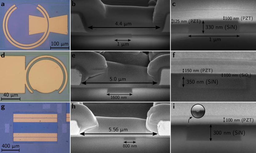
Figs. 1a and 1b show the top view and waveguide cross-section of a C-band ring modulator, for images of the other fabricated modulators (O-band ring, C-band Mach-Zehnder), see Supplementary Information. Fig. 1c shows a schematic of the cross-section. An electric field is applied through in-plane electrodes, changing the refractive index in the PZT and hence the effective index of the waveguide mode. The PZT thin films exhibit a higher refractive index ( 2.3) than \ceSiN ( 2), so a significant portion of the optical mode is confined in the PZT. A grating coupler is used for in- and outcoupling, into the fundamental quasi-TE optical mode.
DC characterization and poling stability
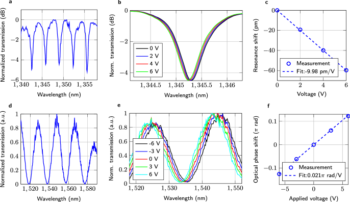
Fig. 1d shows the transmission spectrum of a C-band (1530 nm - 1565 nm) ring modulator. The ring has a loaded factor of 2230 and a free-spectral range 1.7 nm. The ring radius, the length of the phase shifter and the electrode spacing are respectively 100 \textmugreekm, 524 \textmugreekm and 4.4 \textmugreekm. The relatively low factor is caused by sub-optimal alignment of the electrodes.
After deposition the PZT crystallites have one crystal plane parallel to the substrate, but no preferential orientation in the chip’s plane. To obtain a significant electro-optic response for the quasi-TE optical mode, a poling step is performed by applying 60-80 V ( 150 kV/cm) for 1 hour at room temperature, followed by several hours of stabilization time.
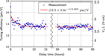
The transmission spectrum is measured for different DC-voltages applied across the PZT layer (Fig. 1e). The voltage-induced index change shifts the resonance. In Fig. 1f, the resonance wavelength shift is plotted as a function of voltage, the slope gives the tuning efficiency pm/V. From this we estimate the half-wave voltage-length product to be Vcm. Through simulation of the optical mode and DC electric field, the effective electro-optic coefficient of the PZT-layer is estimated to be 61 pm/V (see Methods), in good comparison with ellipsometry measurements on our thin films george2015lanthanide . Measurements on other modulator structures yield consistent values for , the smallest value ( Vcm) was measured on an O-band ring (Supplementary Information).
The PZT was poled prior to the measurements, after which no bias voltage was used. To demonstrate longer term stability of the poling, the DC tuning efficiency was periodically measured (sweeping the voltage over [-2,+2] V) on a C-band ring over a total time of almost three days. In Fig. 2, the resulting tuning efficiency is plotted as a function of time, decaying towards a stable value of about -13.5 pm/V over the course of several hours. The poling stabilized and there are no indications of decay over much longer periods of time, hence modulation is possible without a constant bias, as opposed to similar materials like BTO abel2013strong ; xiong2014active ; Eltes2017a .
High-speed characterization
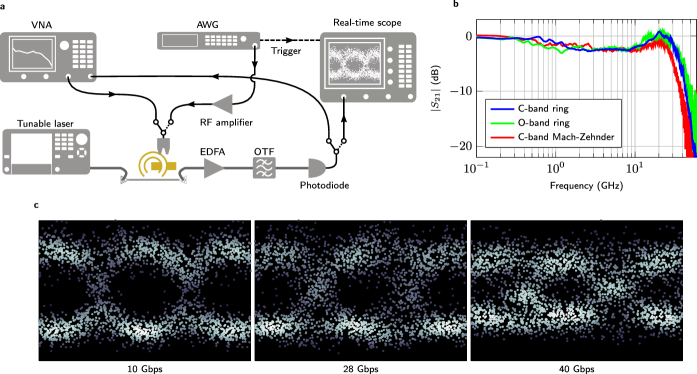
For many applications, high-speed operation is essential. In Fig. 3a the setup used for high-speed characterization is shown. On Fig. 3b, the measurement for different modulators is plotted. The measured 3 dB bandwidths of both rings are around 33 GHz, the Mach-Zehnder has a bandwidth of 27 GHz. The bandwidths are not limited by the intrinsic material response of PZT, but by device design and/or characterization equipment. We furthermore demonstrate that our platform can be used for high-speed data transmission. In Fig. 3c, eye diagrams are plotted for different bitrates, a non-return-to-zero (NRZ) binary sequence (4.2 V peak-to-peak) is used. The eye remains open up until about 40 Gbps, limited by the arbitrary waveform generator (AWG) (25 GHz bandwidth), rather than by the modulator itself. At 10 Gbps, an extinction ratio of 3.1 dB is measured (see Supplementary Information).
Device optimization
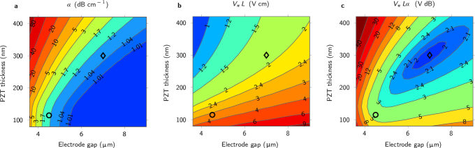
The presented devices were not fully optimized in terms of electro-optic modulation parameters. Primarily the PZT thickness could be increased. Sub-optimal thicknesses were used to reduce bend losses and coupling losses into PZT covered waveguide sections. These limitations can be alleviated by device design. In Fig. 4, simulation results of the most important figures of merit are plotted as function of the PZT layer thickness, and the electrode spacing. Waveguide height, width and the wavelength are respectively 300 nm, 1.2 \textmugreekm and 1550 nm. The waveguide propagation loss (Fig. 4a) is calculated as the sum of a contribution caused by the electrodes, and a constant intrinsic propagation loss of 1 dB/cm, a realistic value if the samples are planarized using CMP (see Supplementary Information). The half-wave voltage-length product (see Methods) and the product are shown in Fig. 4b and 4c, respectively. represents a trade-off between drive voltage and device length, also takes into account loss, and is arguably more important for many applications Jin2018piezoelectrically . The loss increases with decreasing electrode spacing, but also with increasing PZT thickness, since the mode expands laterally. Due to the increasing overlap between the optical mode and the PZT, decreases with increasing thickness. also increases with increasing electrode spacing. An optimization of the waveguide width is given in the Supplementary Information. From Fig. 4b it is clear that can go well below 2 Vcm. The interplay between these different dependencies can be seen in the plot of (Fig. 4b), which shows an optimum with VdB.
Discussion
To conclude, we have demonstrated a novel platform for efficient, optically broadband, high-speed, nano-photonic electro-optic modulators. Using a relatively simple chemical solution deposition procedure we incorporated a thin film of strongly electro-optic PZT onto a SiN-based photonic chip. We demonstrated stable poling of the electro-optic material, and efficient and high-speed modulation, in the absence of a bias voltage. O- and C-band operation was shown, however we expect the platform to be operational into the visible wavelength range (450 nm) rahim2017expanding ; pandey2005structural ; gu2017lanthanum . From simulations it is clear that the devices characterized in this paper do not yet represent the limitations of the platform and VdB is achievable. Moreover, our approach is unique in its versatility, as the PZT film can be deposited on any sufficiently flat surface, enabling the incorporation of the electro-optic films onto other guided-wave platforms.
Methods
PZT deposition and patterning.
The details of the lanthanide-assisted deposition procedure have been published elsewhere george2015lanthanide , a short summary is given here. Intermediate seed layers based on lanthanides are deposited prior to the PZT deposition. The intermediate layer acts as a barrier layer to prevent the inter-diffusion of elements and as a seed layer providing the lattice match to grow highly oriented thin films. A critical thickness of the intermediate layer needs to be maintained ( 5 nm) to avoid diffusion and secondary phase formations. However, on samples with considerable surface topology, thicker intermediate layers are necessary to provide good step coverage and to avoid any issues associated with the conformity in spin-coating. On our samples planarized through etching, step heights between oxide and \ceSiN waveguides varied. We typically used an intermediate layer of thickness 24 nm to avoid issues. Both the intermediate layer and the PZT thin films are deposited by repeating the spin-coating and annealing procedure, which allows easy control of the film thickness. The PZT layer is deposited and annealed at 620 ∘C for 15 min in tube furnace under an oxygen ambient. This Chemical Solution Deposition (CSD) method, also called sol-gel, provides a cheap and flexible alternative to achieve high quality stoichiometric PZT thin films regardless the substrate material. A reactive ion etching (RIE) procedure based on \ceSF6 chemistry is used to pattern the PZT layer. The PZT film was removed selectively over the grating couplers used for the optical measurements.
High-speed measurements.
The small-signal response measurements were performed using an Agilent PNA-X N5247A network analyzer and a high-speed photodiode (Discovery Semiconductors DSC10H Optical Receiver). For the eye diagram measurements, an arbitrary waveform generator (Keysight AWG M8195A) and RF amplifier (SHF S807) are used to apply a pseudorandom non-return-to-zero (NRZ) binary sequence, the modulator output is measured with a Keysight 86100D oscilloscope with 50 GHz bandwidth and Discovery Semiconductors DSC-R409 PIN-TIA Optical Receiver.
Calculation of the electro-optic parameters.
Using COMSOL Multiphysics®, several parameters can be calculated that strongly influence the performance of the modulators. To obtain efficient phase modulation, it is essential to maximize the overlap between the optical mode and the RF electrical signal, quantified by the electro-optic overlap integral koeber2015femtojoule ,
| (1) |
where is the spacing between the electrodes, the applied voltage, the vacuum permittivity, the speed of light in vacuum and the refractive index of PZT. is the in-plane (x-)component of the RF electric field, and represents the in-plane transversal component of the optical field. When used as a phase shifter, an important figure of merit is the half-wave voltage-length product . This product relates to the electro-optic coefficient of the PZT films and to koeber2015femtojoule ,
| (2) |
where is the wavelength. Another important parameter is the propagation loss of the optical mode, consisting of an intrinsic contribution (scattering, material loss in the PZT, intermediate layer, nitride and oxide) and a contribution caused by the vicinity of the electrical contacts. The former can be estimated based on cut-back measurements on unmetalized waveguides (see Supplementary Information), the latter can be numerically calculated.
Acknowledgements
The authors thank Stéphane Clemmen for his overseeing role in the \ceSiN chip fabrication and Philippe F. Smet for help with processing. K. A. is funded by FWO Flanders.
References
- (1) Sun, C. et al. Single-chip microprocessor that communicates directly using light. Nature 528, 534-538 (2015).
- (2) Rahim, A. et al. Expanding the silicon photonics portfolio with silicon nitride photonic integrated circuits. Journal of Lightwave Technology 35, 639–649 (2017).
- (3) Levy, J. S. et al. CMOS-compatible multiple-wavelength oscillator for on-chip optical interconnects. Nature Photonics 4, 37 (2010).
- (4) Bauters, J. F. et al. Ultra-low-loss high-aspect-ratio \ceSi3N4 waveguides. Optics Express 19, 3163–3174 (2011).
- (5) Moss, D. J., Morandotti, R., Gaeta, A. L. & Lipson, M. New CMOS-compatible platforms based on silicon nitride and Hydex for nonlinear optics. Nature Photonics 7, 597 (2013).
- (6) Ramelow, S. et al. Silicon-nitride platform for narrowband entangled photon generation. arXiv preprint arXiv:1508.04358 (2015).
- (7) Kahl, O. et al. Waveguide integrated superconducting single-photon detectors with high internal quantum efficiency at telecom wavelengths. Scientific Reports 5, 10941 (2015).
- (8) Zhuang, L., Roeloffzen, C. G., Hoekman, M., Boller, K.-J. & Lowery, A. J. Programmable photonic signal processor chip for radiofrequency applications. Optica 2, 854–859 (2015).
- (9) Poulton, C. V. et al. Large-scale silicon nitride nanophotonic phased arrays at infrared and visible wavelengths. Optics Letters 42, 21–24 (2017).
- (10) Reed, G. T. et al. High-speed carrier-depletion silicon Mach-Zehnder optical modulators with lateral PN junctions. Frontiers in Physics 2, 77 (2014).
- (11) Xu, Q., Schmidt, B., Pradhan, S. & Lipson, M. Micrometre-scale silicon electro-optic modulator. Nature 435, 325 (2005).
- (12) Liu, A. et al. A high-speed silicon optical modulator based on a metal–oxide–semiconductor capacitor. Nature 427, 615 (2004).
- (13) Hiraki, T. et al. Heterogeneously integrated III–V/Si MOS capacitor Mach–Zehnder modulator. Nature Photonics 11, 482 (2017).
- (14) Han, J.-H. et al. Efficient low-loss InGaAsP/Si hybrid MOS optical modulator. Nature Photonics 11, 486 (2017).
- (15) Liu, M. et al. A graphene-based broadband optical modulator. Nature 474, 64 (2011).
- (16) Sorianello, V. et al. Graphene–silicon phase modulators with gigahertz bandwidth. Nature Photonics 12, 40 (2018).
- (17) Alloatti, L. et al. 100 GHz silicon–organic hybrid modulator. Light: Science & Applications 3, e173 (2014).
- (18) Srinivasan, A. et al. 56 Gb/s germanium waveguide electro-absorption modulator. Journal of Lightwave Technology 34, 419–424 (2016).
- (19) Abel, S. et al. A strong electro-optically active lead-free ferroelectric integrated on silicon. Nature Communications 4, 1671 (2013).
- (20) Xiong, C. et al. Active silicon integrated nanophotonics: ferroelectric \ceBaTiO3-devices. Nano Letters 14, 1419–1425 (2014).
- (21) Eltes, F. et al. A novel 25 Gbps electro-optic Pockels modulator integrated on an advanced \ceSi photonic platform. IEEE International Electron Devices Meeting (IEDM) (2017).
- (22) Xiong, C., Pernice, W. H. & Tang, H. X. Low-loss, silicon integrated, aluminum nitride photonic circuits and their use for electro-optic signal processing. Nano Letters 12, 3562–3568 (2012).
- (23) Wang, C., Zhang, M., Stern, B., Lipson, M. & Lončar, M. Nanophotonic lithium niobate electro-optic modulators. Optics Express 26, 1547–1555 (2018).
- (24) Phare, C. T., Lee, Y.-H. D., Cardenas, J. & Lipson, M. Graphene electro-optic modulator with 30 GHz bandwidth. Nature Photonics 9, 511–514 (2015).
- (25) Hosseini, N. et al. Stress-optic modulator in TriPleX platform using a piezoelectric lead zirconate titanate (PZT) thin film. Optics Express 23, 14018–14026 (2015).
- (26) Jin, W., Polcawich, R. G., Morton, P. A. & Bowers, J. E. Piezoelectrically tuned silicon nitride ring resonator. Optics Express 26, 3174–3187 (2018).
- (27) George, J. et al. Lanthanide-assisted deposition of strongly electro-optic PZT thin films on silicon: toward integrated active nanophotonic devices. ACS Applied Materials & Interfaces 7, 13350–13359 (2015).
- (28) Reed, G. T. et al. Recent breakthroughs in carrier depletion based silicon optical modulators. Nanophotonics 3, 229–245 (2014).
- (29) Pandey, S. et al. Structural, ferroelectric and optical properties of PZT thin films. Physica B: Condensed Matter 369, 135–142 (2005).
- (30) Gu, W., Song, Y., Liu, J. & Wang, F. Lanthanum-based compounds: Electronic bandgap-dependent electro-catalytic materials toward oxygen reduction reaction. Chemistry-A European Journal (2017).
- (31) Koeber, S. et al. Femtojoule electro-optic modulation using a silicon-organic hybrid device. Light: Science & Applications 4, e255 (2015).
Supplementary information
S1 Additional devices
The paper mainly highlights the results on C-band ring resonator modulators. However, more device types have been fabricated and characterized. Apart from the C-band rings, this section provides more details on O-band (1260 nm - 1360 nm) ring modulators and a C-band Mach-Zehnder type modulator. Fig. S1 gives an overview: Figs. S1a-c show respectively the top-view, cross section and a detailed cross section of the C-band device described in the paper, whereas Figs. S1d-f and S1g-i do the same for an O-band ring and a C-band Mach-Zehnder Interferometer (MZI). The O-band ring has a -factor of 1820 and a free-spectral range of 3.27 nm. The ring radius is 40 \textmugreekm, with a phase shifter length of 195 \textmugreekm. The MZI modulator electrodes have a length of 1 mm. Note the differences between the cross-sections of the devices, the waveguides in Figs. S1c and S1i were planarized trough back-etching of the top ( 1 \textmugreekm thick) oxide using a combination of reactive ion etching (RIE) and wet etching (HF), variations in top oxide thickness, etch rates and exact etch times can lead to relatively large steps (Fig. S1c). Moreover, the etch rates of the deposited oxide depend on the exact nitride structures underneath, even in the case of a seemingly planar surface (Fig. S1i), trenches of several tens of nanometers arise next to the waveguide (see inset in Fig. S1i). On Fig. S1d-f however, a device planarized using chemical mechanical polishing (CMP) is shown. A buffer layer of 50-100 nm of oxide is left on top of the nitride waveguide, so the obtained surface is much smoother. This leads to much smaller propagation losses (see section S2).
Figs. S2a-c respectively show the transmission spectrum of the O-band ring (pictures in Figs. S1d-f), its transmission spectrum for different DC-voltages, and the resonance shift as a function of voltage. The linear fit on Fig. S2c shows a resonance tuning efficiency of pm/V. From this value the half-wave voltage-length product can be estimated: Vcm. Through simulation of the optical mode and DC electric field, the effective electro-optic coefficient of the PZT-layer around 1310 nm is estimated to be about 67 pm/V (see Methods).
Figs. S2d-f show the transmission spectrum of the MZI modulator (pictures in Figs. S1g-i), the transmission spectrum for different voltages applied across the PZT and the electro-optic phase shift (with respect to 0 V) as a function of voltage. The voltage is applied to only one of the MZI arms. From this, we can estimate the (voltage needed to induce a phase shift, or a shift of the sinusoidal transmission pattern over half a period) to be 47.6 V, corresponding to a of 4.76 Vcm. This corresponds to an of the PZT-layer of about 70 pm/V.
Variations in the measured values are mainly due to variations in the waveguide cross-sections, electrode spacings and the used wavelengths (C-band versus O-band), see Eq. (2). Extracted electro-optic coefficients also vary somewhat, differences can in part be due to variations in film quality on different samples, but mainly stem from small uncertainties on the exact cross-section dimensions.
S2 Waveguide loss measurements
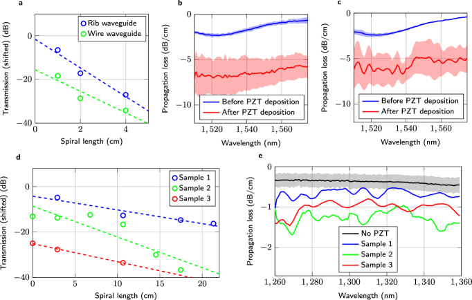
In Fig. S3 the loss measurements on different types of waveguides are summarized. For the C-band measurements, chips were planarized using a combination of reactive ion etching (RIE) and wet hydrogen fluoride (HF) etching. Typically resulting in steps and trenches of several tens of nanometers in the vicinity of the waveguide (see section S1 and Fig. S1c, i). Figs. S3a-c summarize loss measurements on such waveguides, for a set of rib waveguide spirals (blue line on Fig. S3a and Fig. S3b) and a set of wire waveguide spirals (green line on Fig. S3a and Fig. S3c). The PZT-covered wire waveguides, resembling the ones used in the C-band modulators, have an estimated loss of 5 to 6 dB/cm. The rib waveguides were defined using a partial etch of 220 nm next to the waveguide core, the influence of this on the propagation loss is only expected to be minor, as is demonstrated by the measurements. Note that before PZT deposition, the waveguide loss can be as low as 0.5 dB/cm. For the O-band measurements, the planarization of the waveguides was done by chemical-mechanical polishing (CMP), resulting in a waveguide cross-section as shown in Fig. S1f, with a residual oxide layer of 50 to 100 nm on top of the waveguide (see section S1). Figs. S3d-e show the loss measurements of such waveguides for 3 test samples. The smoother surface for the PZT deposition can result in losses below 1 dB/cm. The simulated confinement factor in the PZT layer for the C- and O-band waveguides used in the loss measurements are respectively (for both rib and wire waveguides) and .
S3 Extinction ratio measurement
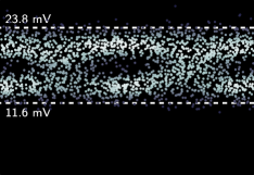
The eye diagram shown in Fig. S4 was obtained using a DC-coupled Tectronix 80 C02-CR optical receiver with a sampling oscilloscope (Tektronix CSA 8000), applying a peak-to-peak voltage of 4.2 V at 10 Gbps (same as for Fig. 2c). Since the measured voltage scales with the total optical power, we can estimate the extinction ratio to be about . This corresponds well with a simple ball-park estimate based on the observed transmission spectrum and static DC-shift (Figs. 1d, e), since the extinction ratio in DC can be estimated as , where is the transmission expressed in dB.
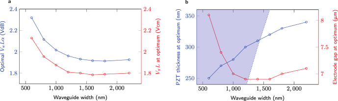
S4 Device optimization - influence of the waveguide width
In the simulations in Fig. 4, a sweep of the electrode spacing and PZT thickness was performed, since these can be easily tailored in post-processing. This was done for a fixed waveguide width of 1.2 \textmugreekm. The waveguide width can however also be designed, an optimization is given here. At each width, a sweep of as a function of PZT thickness and electrode gap of the kind described in the main text and shown in Fig. 4 was performed. Fig. S5a shows the optimal (smallest) value and the at that optimum. Fig. S5b shows the PZT thickness and electrode spacing of this optimum. The light blue area shows the waveguide width/PZT thickness combinations for which the waveguide only supports a single TE mode. In the main text, a width of 1.2 \textmugreekm was chosen in order to minimize whilst still having single-mode behavior at the optimal point.