Exciton states in monolayer MoSe2 and MoTe2 probed by upconversion spectroscopy
Abstract
Transitions metal dichalcogenides (TMDs) are direct semiconductors in the atomic monolayer (ML) limit with fascinating optical and spin-valley properties. The strong optical absorption of up to 20 % for a single ML is governed by excitons, electron-hole pairs bound by Coulomb attraction. Excited exciton states in MoSe2 and MoTe2 monolayers have so far been elusive due to their low oscillator strength and strong inhomogeneous broadening. Here we show that encapsulation in hexagonal boron nitride results in emission line width of the A:1 exciton below 1.5 meV and 3 meV in our MoSe2 and MoTe2 monolayer samples, respectively. This allows us to investigate the excited exciton states by photoluminescence upconversion spectroscopy for both monolayer materials. The excitation laser is tuned into resonance with the A:1 transition and we observe emission of excited exciton states up to 200 meV above the laser energy. We demonstrate bias control of the efficiency of this non-linear optical process. At the origin of upconversion our model calculations suggest an exciton-exciton (Auger) scattering mechanism specific to TMD MLs involving an excited conduction band thus generating high energy excitons with small wave-vectors. The optical transitions are further investigated by white light reflectivity, photoluminescence excitation and resonant Raman scattering confirming their origin as excited excitonic states in monolayer thin semiconductors.
I Introduction
Transition metal dichalcogenides such as MoS2, WS2, WSe2, MoSe2 and MoTe2 are direct band gap semiconductors when thinned down to one monolayer Novoselov:2016a ; Geim:2013a ; Mak:2010a ; Splendiani:2010a ; Wang:2012c ; Mak:2016a . Their bandgap is situated in the visible to near infrared of the optical spectrum. Since the Coulomb interaction is strong in this ultimate 2D limit, the optical properties are dominated by excitons, bound electron-hole pairs Wang:2017b ; He:2014a ; Ugeda:2014a ; Chernikov:2014a ; Ye:2014a ; Qiu:2013a ; Ramasubramaniam:2012a ; Wang:2015b . Recently encapsulation in hexagonal boron nitride (hBN) of TMD monolayers (MLs) has resulted in considerable narrowing of the exciton transition linewidth down to 1 meV Jin:2016a ; Manca:2017a ; Chow:2017a ; Cadiz:2017a ; Ajayi:2017a ; Wang:2016v ; wierzbowski2017direct . This gives now access to fine features of the exciton spectra that dominate the linear and non-linear optical properties.
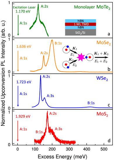
Optical excitation of a semiconductor at the bandgap typically results in luminescence at lower energy due to energy relaxation of charge carriers and excitons. In Fig. 1a-d we show that resonant laser excitation of the lowest energy exciton resonance A:1 results in pronounced photoluminescence (PL) emission at higher energy than the excitation laser for four different TMD ML materials. This effect is generally termed upconversion and has been observed for different semiconductor structures such as InP/InAs heterojunctions, CdTe quantum wells and InAs quantum dots Seidel:1994a ; Hellmann:1995a ; Poles:1999a ; Paskov:2000a ; Chen:2012a albeit based on different microscopic mechanisms. Upconversion has previously been reported for WSe2 Manca:2017a ; Jones:2015a and MoS2 Robert:2018a MLs. These experiments allow detailed insight into the light matter interaction physics of excitons in TMD monolayers: First, clarifying the origin of upconversion signal is in itself a crucial problem, as the origin of excess energy needs to be identified and the role of exciton-exciton scattering mechanisms is revealed. Second, upconversion spectroscopy gives us access to the excited exciton states that govern absorption and emission, so far not well understood in ML MoSe2 and MoTe2. The centre of mass motion of excitons, in analogy to the hydrogen atom and positronium, is characterized by a principle quantum number , where typical photoluminescence emission stems from the exciton of the A-exciton series, labelled A:1. The optical absorption in energy above the A:1 optical transition will be determined by the excited states A:2 etc and the B-exciton series, separated from the A-exciton mainly by the spin-orbit splitting in the 200-400 meV range Kormanyos:2015a . We show that upconversion allows us to access excited exciton states for MoSe2 and MoTe2, which is not possible in samples that are not encapsulated in hBN as the excited A-excitons spectrally overlap with the B-exciton series. We demonstrate bias control of the upconversion process. We provide an in-depth study of exciton states in MoTe2 comparing upconversion with photoluminescence excitation spectroscopy (PLE) and white light reflectivity. In the last part of the paper we provide a theoretical model and discuss the origin of upconversion in TMD monolayers. Our model calculations suggest that Auger type exciton-exciton scattering is very efficient in TMD MLs as compared to other semiconductor nano-structures due to (i) the strong Coulomb interaction, which makes it possible to relax the single-electron momentum conservation PhysRevB.54.16625 ; PhysRevB.73.245424 and (ii) the possibility of a resonant processes involving exciton transfer to an excited energy band.
II Excited state spectroscopy in ML
Monolayer MoSe2 is a very versatile TMD material ideally suited to explore coupling to optical cavities dufferwiel2017valley ; lundt2016monolayered , investigating voltage control of monolayer mirrors Scuri:2018a ; back2017giant and interplay between charged and neutral excitons hao2016coherent . Most of these experiments are based on the optical response of the lowest energy exciton state A:1, but very little is known about excited exciton states that govern optical absorption at higher energies and energy relaxation pathways for PL emission.
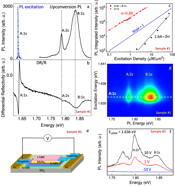
The experimental results for the high quality MoSe2 samples encapsulated in hBN Taniguchi:2007a are summarized in Fig. 2, details of the experimental set-up can be found in Appendix A. In differential white light reflectivity at T K, we clearly observe the A and B-exciton states Ross:2013a ; Wang:2015a ; Wang:2015c , the A: resonance has a full width at half maximum (FWHM) of the order of 2 meV shree2018exciton .
In Fig. 2a we show an intriguing result: excitation of the sample with a low power, continues wave (cw), narrow linewidth (eV) laser at the A: energy results in emission of the B: transition at higher energy. As we scan the laser across the A:1 resonance, the PL intensity (black graph) has a clear maximum in intensity when the laser is exaclty at the A:1 resonance, the blue data points represent the integrated upconversion intensity for different laser energies. An additional transition to B:1 appears about 150 meV above the A: in upconversion PL that we tentatively assign to the excited A-exciton, A:2 state. This transition is also visible in reflectivity in Fig. 2b. For samples directly exfoliated onto SiO2 the excited A-exciton states were not directly accessible due to their overlap with the B-exciton state. A fingerprint of the A: state was reported in two-photon PL excitation (PLE) experiments Wang:2015c , where the B: state absorption is strongly reduced Glazov:2017a .
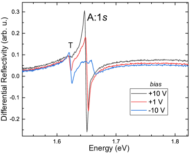
Now we investigate the origin of the upconversion PL in ML MoSe2 shown in Figs. 1b and 2a. We compare the evolution of standard and upconversion PL intensity as a function of laser power in Fig. 2c . The slope of the upconversion intensity versus laser power () is roughly twice as high as for standard PL (), consistent with a two-photon (two exciton) process being at the origin of this non-linear optical effect. In Fig. 2d we plot the upconversion emission as the laser is scanned across the A:1 resonance. Upconversion is only detectable over a 2 meV range of laser energy when the laser is in resonance with the A: state. This indicates upconversion is a resonant process, as observed for WSe2 monolayers Manca:2017a . This conclusion gets additional support from upconversion experiments in a charge tunable device (Fig. 2e), presented in Fig. 2f. At a bias of +10 V, the excitation laser is tuned into resonance with the neutral A: state. As the applied voltage is lowered to +1 V, electrons are added to the monolayer, decreasing absorption strength at the neutral exciton resonance. The upconversion signal is not detectable any more for a bias of V as absorption at the exciton resonance is inefficient, as the charged exciton absorption, at a different energy, dominates Scuri:2018a ; back2017giant ; Ross:2013a . Differential reflectivity of our device shows a strong neutral exciton resonance at +10 V whereas for V the charged exciton transition dominates, see Reflectivity measurements on the device in Appendix B. These experiments confirm that upconversion PL emission has its origin in resonant neutral exciton generation and can be controlled electrically in charge tunable structures.
III Excited state spectroscopy in ML
MoTe2 is a very interesting layered material bie2017mote ; jiang2017zeeman , which provides the fascinating opportunity to switch between semiconducting and metallic phases by tuning strain or carrier concentration Song:2015a ; Li:2016a . This allows working towards devices based on bias controlled phase changes in monolayer MoTe2 Wang:2017mote2 ; doi:10.1021/acs.nanolett.6b04814 . First studies of MoTe2 flakes exfoliated on SiO2 have identified monolayers as direct semiconductors Ruppert:2014a ; Lezama:2015a , interestingly the nature of the gap of the bilayer is still under discussion Robert:2016b ; PhysRevB.94.085429 . So in practice the difference between mono- and bilayers has to be confirmed in Raman experiments, see Fig. S2a. MoTe2 MLs have an optical bandgap at T K at 1.17eV corresponding to an emission wavelength of 1050 nm. Therefore, its alloying with other TMD materials such as MoS2 and MoSe2 allows in principle to cover the full spectral range from 630 to 1050 nm for optoelectronics applications. As optical absorption is not only strong at the excitonic bandgap (A:1) but also for higher lying exciton states Wang:2017b ; He:2014a ; Ugeda:2014a ; Chernikov:2014a ; Ye:2014a ; Qiu:2013a ; Ramasubramaniam:2012a ; Wang:2015b better knowledge of the excited exciton spectrum is needed. This allows also in principle to get an estimation of the exciton binding energy, by trying to compare with model calculations of exciton states in a screened 2D potential Rytova:1967 ; Keldysh:1979a ; Chernikov:2014a ; Robert:2018a .
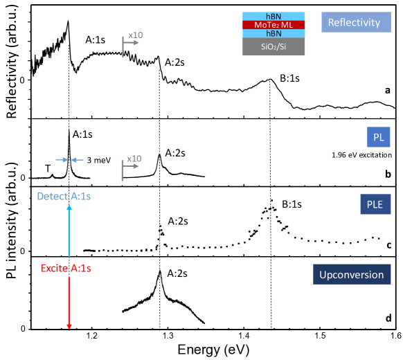
Here we show the striking impact of hBN encapsulation on the optical properties of monolayer MoTe2. The PL spectrum in Fig. 3b shows very narrow emission lines (FWHM linewidth of 3 meV) for the neutral exciton at the A: state at 1.17 eV, approaching the optical quality reported for hBN encapsulated MoS2 and WSe2 monolayers Jin:2016a ; Manca:2017a ; Chow:2017a ; Cadiz:2017a ; Ajayi:2017a ; Wang:2016v ; wierzbowski2017direct . We confirm the high sample quality in reflectivity experiments in Fig. 3a, that show this transition basically at the same energy as in PL, indicating negligible neutral exciton localization. In reflectivity we see also a broader transition about 250 meV above the A: that we ascribe to the B: state, following comparison with the data from the literature Ruppert:2014a ; Lezama:2015a ; yang2015robust . We also observe in reflectivity a transition 120 meV above the A: state, not reported previously, which we ascribe to the A: state. Strikingly, when exciting with a laser energy of 1.96 eV we also see hot PL emission of this A:2 transition in Fig. 3b.
To further investigate the nature of these excited exciton states, we carry out PLE experiments. We monitor the PL emission of the A: state (as in Fig. 3b) as a function of the laser excitation power. PLE probes absorption, which gives information on the higher lying electronic transitions, and subsequent relaxation to the A: state, usually by emitting phonons. We observe in our experiments clear indications of both processes: absorption by excited exciton states and phonon assisted energy relaxation. In Fig. 3c, we see clear resonances in PLE exactly at the same energies as the reflectivity spectrum for the A:2 and B:1 state. The PL emission is enhanced by orders of magnitude where the laser is resonant with these excited exciton states, indicating efficient absorption and energy relaxation. More details on phonon assisted relaxation and associated Raman scattering on this sample are described in Appendix B.
As discussed in the previous section for MoSe2 MLs, a powerful technique for investigating exciton states is photoluminescence upconversion. Here a cw laser excites the MoTe2 monolayer at the A: resonance and emission at higher energies is monitored. In Fig. 3d we indeed observe emission 120 meV above the A: state, this emission is exactly at the same energy as the transition ascribed to the A: state with the three other spectroscopy techniques: reflectivity, hot PL and PLE all compared in Fig. 3a-d.
To summarize the main experimental results, we have demonstrated that TMD MLs such as MoTe2, MoSe2, MoS2 and WSe2 exhibit strong photoluminescence upconversion. At resonant laser excitation of the A: ground excitonic state luminescence from excited states, such as A: and B: is detected. The effect vanishes for non-resonant excitation or if the oscillator strength of the A: exciton is reduced by the gate-doping in charge tunable samples. Furthermore, the analysis of the upconversion PL intensity as a function of excitation power demonstrates that this effect is non-linear and requires two excitons in the ground state. In the next section we provide a theoretical model for our findings.
IV Theory of exciton upconversion
In this section we provide a theoretical model of the upconversion effect observed in TMD MLs. In this process the emitted photon energy is larger than that of the absorbed photon. That is why, in order to fulfil energy conservation, a third body, an exciton or a phonon should be involved. However, at a temperature of K the thermal phonon energies are less than meV, thus, lattice vibrations cannot provide effective transfer of excitons up to several meV above the excitation energy. Additionally, experimental data shown in Fig. 2c (see also Ref. Manca:2017a ) clearly demonstrates the presence of an optical nonlinearity: The upconversion intensity scales quadratically with the number of photoexcited excitons. Thus, in order to describe the upconversion theoretically we need to take into account exciton-exciton interaction processes where one of the excitons is annihilated while the second exciton acquires large extra energy, as depicted in the inset in Fig 1b Mouri:2014a ; Kumar:2014b . Subsequently, this exciton relaxes toward the radiative states (particularly, A: and B:) and hot luminescence from these states is observed since the radiative recombination time is competitive (i.e. short enough) compared to the energy relaxation time.
This mechanism of generating highly excited excitons can be viewed as Auger-like exciton-exciton annihilation. At first glance, it seems to be quite weak because in order to satisfy the energy and momentum conservation laws, the initial kinetic energy of the involved particles should be very large abakumov_perel_yassievich . As we show here this effect is very efficient in TMD MLs due to (i) strong Coulomb interaction, which makes it possible to relax the single-electron momentum conservation PhysRevB.54.16625 ; PhysRevB.73.245424 and (ii) the possibility of a resonant processes involving exciton transfer to an excited energy band Manca:2017a . In other words, we try to include the particular energy spacing between different conduction bands in the theory of this four particle interaction.
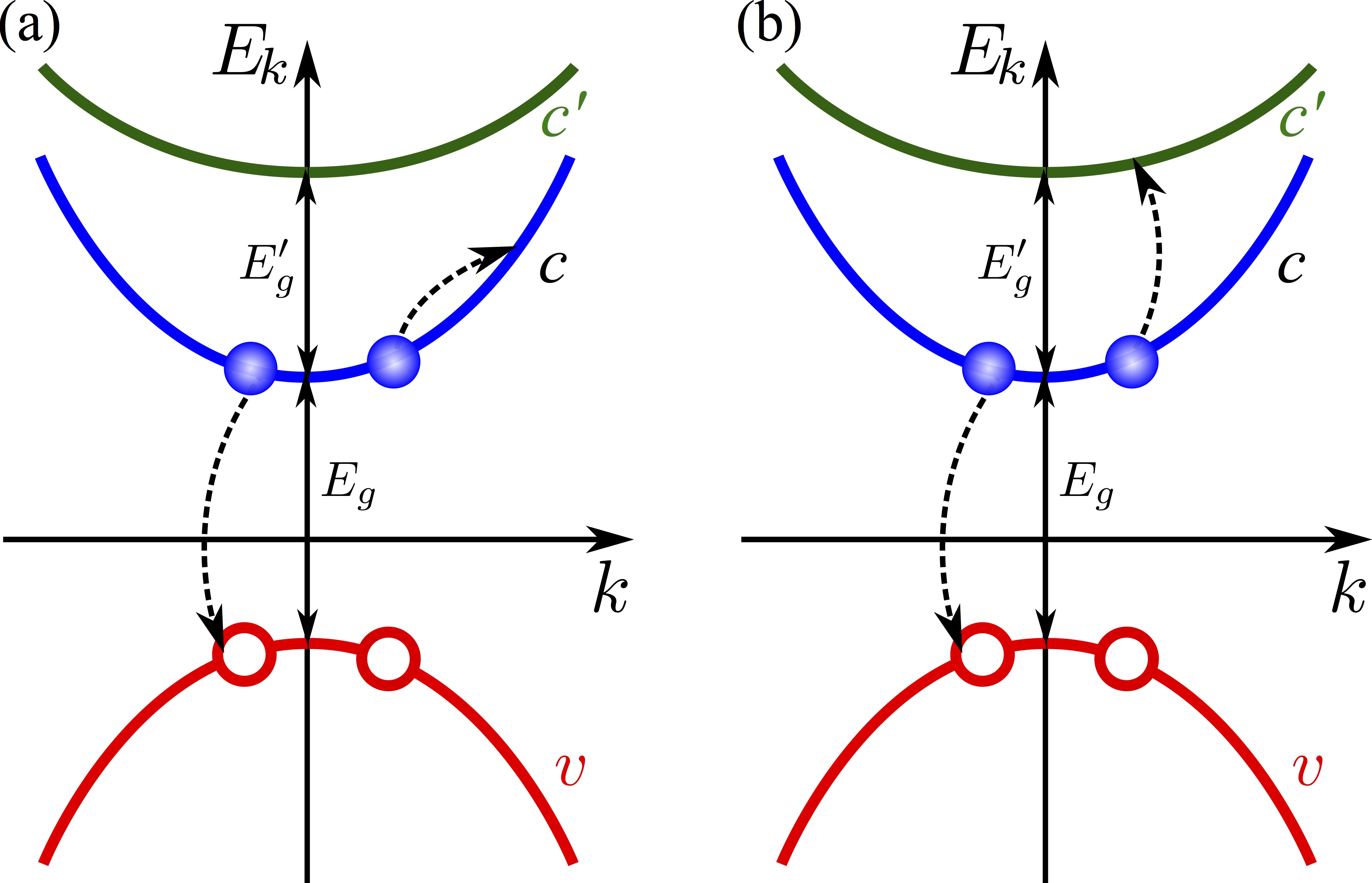
The schematics of exciton-exciton Auger processes is presented in Fig. 4. Panel (a) shows an example of a standard Auger process which is possible in any semiconductor: Due to the Coulomb interaction one electron recombines with a hole, while another carrier is transferred to a highly excited state. Figure 4(b) illustrate a very different process, which is possible in the studied TMD MLs due to their specific band structure: It turns out that there is an excited conduction band (denoted as ) whose distance to the conduction band, , approximately satisfies the condition
| (1) |
where eV Wang:2017b is the exciton binding energy, see Tab. 1. Thus, in the course of exciton-exciton annihilation the electron can be promoted to the band with relatively small wavevector rather than be scattered to a large wavevector state within the same band.
| Energy (eV) | MoS2 | MoSe2 | WSe2 | MoTe2 |
|---|---|---|---|---|
The rate of the Auger processes is described by a parameter such that the generation rate of highly energetic excitons is given by
| (2) |
Here is the density of highly energetic excitons, is the density of photoexcited excitons in A: state, recombination and energy relaxation processes are disregarded in Eq. (2). The same rate describes the decay rate of A: excitons due to the non-radiative exciton-exciton annihilation: abakumov_perel_yassievich ; PhysRevB.54.16625 ; Kumar:2014b ; Mouri:2014a ; Sun:2014a ; PhysRevB.93.201111 ; doi:10.1021/acs.jpclett.7b00885 ; PhysRevB.95.241403 ; PhysRevB.94.085429 . The rate can be expressed by means of the Fermi golden rule in the form
| (3) |
Here is the matrix element of the exciton-exciton interaction, and are the center of mass wavevectors of the two interacting excitons, is the distribution function of photoexcited A: excitons, is the exciton dispersion with being its effective mass, the subscript denotes the quantum numbers of the final exciton state which include the electron band index [ or for the processes shown, respectively, in Fig. 4(a) or (b)] as well as of the internal motion (, , …including the continuum states), is the dispersion of the exciton in the final state, which accounts for its binding energy. The exciton wavevector in the final state, is found from the momentum conservation law: . For the derivation of Eq. (3) we assumed that the occupation of the final states is negligible and omitted the corresponding occupation factor and also disregarded the anisotropy and nonparabolicity of exciton dispersion.
The analytical results are obtained in Appendix C under the model assumptions , which allow us to make use of -perturbation theory for calculating the excitonic states and transition rates Glazov:2017a . The analysis demonstrates that the dominating contribution to is given by the resonant processes described in Fig. 4b where the electron in the exciton is promoted to the excited band . The Coulomb interaction between the electrons can result in the process shown in Fig. 4(b) where one pair recombines while the remaining electron occurs in the band. So, one pair is present in the end. Since in this process both electrons change their quantum states the resonant Auger scattering is due to the electron-electron interaction only, while the electron-hole interaction does not play a role. Moreover, our analysis shows that the exchange contribution to the matrix element dominates, see Appendix C.
Our next target is to evaluate the scattering rate for exctions under the resonant condition , where the energy released at the non-radiative recombination of A: exciton with is equal to the energy of the excited -band exciton in the -state. Neglecting the difference of exciton masses in the initial and final states and assuming that excitons are thermalized with the temperature we have
| (4) |
Here is the Boltzmann constant, is the exciton Bohr radius and are the interband momentum matrix elements (in the units of , being the free electron mass) for electron transition from to, respectively, and bands, is the effective high-frequency dielectric constant. In Eq. (4) is the dimensionless overlap integral which depends on the screening parameter of the Coulomb potential given by the Fourier transform , see Appendix C for details. The values of for several excitonic states are shown in Fig. 5. For and reasonable material parameters PhysRevB.95.155406 the quantity at K in Eq. (4) can be estimated to be cm2/s. This quantity can be reduced by a factor if the resonant condition is not fulfilled. The rate of intraband transitions, where the electron remains in the same band, Fig. 4(a), can be estimated by replacing the factor by which produces a parametrically smaller, contribution, see Appendix C. In the non-resonant case where at the resonant transition is not possible and the detuning is present for the intraband process. This intraband process is a only possible when excitons with the kinetic energy on the order of are present. The rate Eq. (4) acquires therefore an exponential factor .
The experimentally observed Auger rates in the literature are one-two orders of magnitude smaller than the resonant contribution to investigated here Kumar:2014b ; Mouri:2014a ; Sun:2014a ; PhysRevB.93.201111 ; doi:10.1021/acs.jpclett.7b00885 ; PhysRevB.95.241403 ; Robert:2016a . The exact values of will also vary with sample temperature and environment, demonstrating that the exact resonance conditions are not fulfilled in the studied structures. Our experiments are carried out at 4 K whereas many exciton-exciton scattering studies are carried out at elevated temperatures. The presence of disorder in the sample, especially without hBN encapsulation, may enable to fulfil simultaneously the energy and momentum conservation in TMD MLs making additional scenarios possible.
To summarize, our analysis suggests that exciton upconversion photoluminescence in TMD MLs is due to a specific nonlinear process: Two excitons generated by the resonant laser collide, as a result one of those recombines non-radiatively while the other is promoted to a highly excited state (most likely related to an excited conduction subband according to band structure calculation). Subsequently, the excited exciton loses its energy and a hot PL from the radiative A: and B: states is observed. This scenario describes the main experimental findings: (i) upconversion PL from the states A: and B: which are visible in the hot PL [Figs. 1, 2(a,b,d) and 3], (ii) quadratic dependence of the upconversion intensity on the number of excitons in the ground state, Fig. 2(c), (iii) resonant character of the process as a function of excitation laser energy, Fig. 2(d), and (iv) absence of the upconversion in the presence of doping, where the exciton resonance vanishes, Fig. 2(f).
V Conclusion
We identify of excited exciton states in high quality MoSe2 and MoTe2 monolayer samples, which govern absorption and emission above the A:1 exciton resonance. We identify the A:2 state 150 meV (120 meV) above the A:1 state in ML MoSe2 (MoTe2). We show that excited exciton states can be studied in photoluminescence upconversion experiments. In addition to being a highly selective spectroscopic tool applicable to several TMD materials Manca:2017a ; Robert:2018a , this non-linear optical effect also gives insights into exciton-exciton interactions, relevant physical processes also for studying population inversion and other density dependent phenomena Li:2017a ; Wu:2015b ; Chernikov:2015z ; PhysRevB.95.241403 . Our work suggests that in TMD monolayers the generation of high energy excitons with Auger-like scattering processes is efficient due to the strong Coulomb interaction and resonant excitation of higher lying conduction bands.
Acknowledgements.
We acknowledge funding from ANR 2D-vdW-Spin, ANR VallEx, Labex NEXT projects VWspin and MILO, ITN Spin-NANO Marie Sklodowska-Curie grant agreement No 676108 and ITN 4PHOTON Nr. 721394. X.M. also acknowledges the Institut Universitaire de France. Growth of hexagonal boron nitride crystals was supported by the Elemental Strategy Initiative conducted by the MEXT, Japan and the CREST (JPMJCR15F3), JST. L.E.G. and M.M.G. acknowledge partial support from LIA ILNACS, RFBR projects 17-02-00383, 17-52-16020, RF President Grant MD-1555.2017.2 and “BASIS” foundation.Appendix A Experimental Methods
The samples are fabricated by mechanical exfoiliation of bulk MoSe2 and MoTe2 (commercially available from 2D semiconductors) and very high quality Hexagonal Boron Nitride (hBN) crystals Taniguchi:2007a on 83 nm SiO2 on a Si substrate. The experiments are carried out at T = 4 K in a confocal microscope built in a vibration free, closed cycle cryostat. The excitation/detection spot diameter is . The monolayer (ML) is excited by continuous wave Ti-Sa laser (700-1020 nm) or a HeNe laser (633 nm). The photoluminescence (PL) signal is dispersed in a spectrometer and detected with a Si-CCD camera () or InGaAs detector (). The typical excitation power is 3 .
Appendix B Additional data
Charge tunening in ML MoSe2. Figure S1 demonstrates reflectivity spectrum of the charge tunable MoSe2 device clearly showing the redistribution of the oscillator strength between the neutral and charged excitons, studied in the context of upconversion in Fig. 2(e,f).
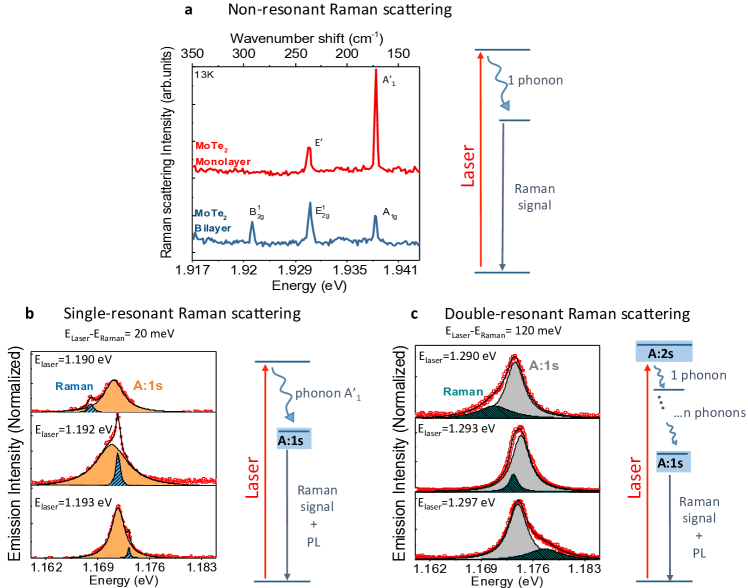
Resonant and non-resonant Raman scattering in ML MoTe2. Scattering with phonons in Raman processes allows to distinguish monolayers from multilayers. This is especially useful for MoTe2 where also the bilayer shows clear and narrow PL emission. In Fig. S2a we compare results for a monolayer and a bilayer, the absence of the peak allows us to identify monolayer samples Guo:2015a ; tonndorf:2013a . The experiments in Fig. S2a are based essentially on non-resonant Raman scattering i.e. neither the laser energy nor the emitted light after phonon scattering are resonant with an particular electronic state. This is different in Fig. S2b : Here we tune the laser to an excess energy of about 20 meV above the A:1 resonance. In addition to PL emission (orange peak) we see a spectrally sharper feature (shaded blue) superimposed on the PL, which shifts with excitation laser energy. This peak is corresponds to Raman scattering with the phonon, which is particularly efficient as the final state after scattering corresponds to a real electronic state Guo:2015a ; Carvalho:2015a ; Wang:2015g ; Chow:2017a ; molas2017raman ; Soubelet:2016a in these single-resonant Raman scattering experiments.
In Fig. S2c we report double resonant Raman experiments Wang:2015g . As the laser energy is scanned across the A: state, we see that the PL of the A: exciton is enhanced, see intensity plotted in Fig. 3c as a function of laser energy. In addition, we
observe in Fig. S2c that a Raman feature is crossing the PL line, exactly 120 meV below the respective laser energy. When the laser is at the A: energy, the Raman process is double resonant Guo:2015a ; Wang:2015g as the initial state (A:) and the final state (A:) are real electronic states. This has already been observed between exciton states in ML WSe2 on SiO2 Wang:2015g . Please note that very different electronic states and phonons are discussed in the double resonant Raman experiments in Ref. Guo:2015a . In experiments in hBN encapsulated ML WSe2 samples the similar experiments have been interpreted as being due to phonon related processes only Jin:2016a . This interpretation seems unlikely in view of follow-up studies of ML WSe2 in magnetic fields, that clearly showed that the excited state is an excitonic transition and not just phonon replica Stier:2018a . For the case of MoTe2 we have a strong case for the transition at 120 meV above the A: to be attributed to a real electronic transition, as this transition is confirmed in Fig. 3a-d by four complementary spectroscopy techniques and in Fig. S2c by double resonant Raman scattering.
Appendix C Calculations of the Auger rates
C.1 Resonant interband process
We consider three bands, , schematically illustrated in Fig. 4 with two excited electron-hole pairs (excitons) with an electron occupying the lowest conduction band and with an empty state in the valence band . Here for simplicity we disregard the spin degree of freedom of change carriers, assuming that the spin is conserved in the course of exciton-exciton interaction. Furthermore, we focus on the states in the vicinity of one of the band extrema ( or valley) and disregard here the processes involving intervalley transfer of electron-hole pair studied in Refs. Glazov:2014a . The Coulomb interaction between the electrons can result in the process shown in Fig. 4(b) where one pair recombines while the remaining electron occurs in the band. So, one pair is present in the end. Since in this process both electrons change their quantum states the resonant Auger scattering is due to the electron-electron interaction only, while, e.g., electron-hole interaction does not play a role.
In the free-particle picture, we have two electrons in the band which occur in the - and -bands after the Coulomb scattering. The two-electron wavefunctions of the considered system in the initial and final states can be presented as
| (5) | ||||
Here , are the electron and unoccupied state wavevectors in one of the excitons and , are the electron and unoccupied state wavevectors in another exciton. The wavefunction in each band is a product of the Bloch amplitude and the plane wave:
| (6) |
and the normalization area is set to unity. In the model, the Bloch amplitudes have the form:
| (7) | |||
| (8) | |||
| (9) |
where denotes the Bloch amplitude at the extremum point, is the free electron mass and are the momentum matrix elements between the states in the bands and ().
The wavefunctions , in Eq. (5) are antisymmetrized with respect to the permutations of electrons. It gives rise to the direct and exchange contributions. The matrix element of the direct interaction, where the electron from the state with the wavevector recombines with the hole from same exciton and transfers to the state , can be conveniently presented in the form
| (10) |
where is the exciton center of mass momentum (note that the hole state corresponds to the time-reversed counterpart of the unoccupied state)
| (11) |
is the 2D Fourier image of the Coulomb potential with being the background average constant of the surrounding structure and being the dielectric screening parameter Rytova:1967 ; Keldysh:1979a ; Cudazzo:2011a . Note that this parameter should be taken in the high-frequency limit because the energy transferred in the course of exciton-exciton interaction is on the order of the band gap .
Taking into account that
| (12) |
where and are the band structure parameters introduced in Refs. Kormanyos:2015a ; PhysRevB.95.155406 and , we obtain:
| (13) |
Finally, the direct interaction matrix element takes a simple form
| (14) |
With account for the excitonic effect Eq. (14) should be averaged over the exciton wavefunction birpikus_eng ; Glazov:2014a ; Glazov:2017a . Furthermore, we need to take into account that in the initial state there are two unoccupied states in the valence band. As a result, we have ()
| (15) |
We recall that , are the wavevectors of excitons in the initial state, is the wavevector of the exciton in the final state, the subscript enumerates the relative motion states of the remaining electron-hole pair. In derivation of Eq. (15) we neglected the difference of electron effective masses in and bands and assumed that initially both excitons occupy state, is the envelope function of the relative motion. Correspondingly, the final state relative motion envelope function remains the same.
Typical center of mass wavevectors involved in exciton-exciton scattering are on the order of thermal wavevector and are much smaller than the screening wavevector , therefore the direct exciton-exciton scattering matrix element is proportional to the first powers of the exciton wavevectors: .
Here we consider an exchange process, where the electron occupies the empty state in the valence band related to the hole in the other exciton, i.e. the electron with the wavevector transfers to the valence band state with the wavevector . As a result for uncorrelated electron-hole pairs we have for the exchange contribution
| (16) |
where is defined in Eq. (14). In order to transform Eq. (16) to the form convenient for averaging over the exciton wavefunctions we introduce the relative motion wavevectors for two initial and final exciton states in accordance with
| (17) |
Here we assumed that the effective masses of the electron and hole are the same in agreement with microscopic calculations Kormanyos:2015a ; PhysRevB.95.155406 . Taking into account that, as before, the center of mass wavevectors are small compared with the inverse Bohr radius of exciton we omit in and in and arrive at
| (18) |
Here are the Fourier transforms of the relative motion exciton functions :
It follows from Eq. (18) that only -shell states contribute to the matrix element. As compared with its direct counterpart, the transferred momentum here is . Since for , the direct contribution is by a factor smaller than the exchange one. Thus, in what follows we consider the exchange contribution only.
In order to analyze the exchange process in more detail we first consider a limit where the screening is very strong, i.e., where . In this case we can approximate by a constant and arrive at
| (19) |
For arbitrary screening we evaluate the sum in Eq. (18) making use of the two-dimensional hydrogenic functions. For the bound states we have chao:6530
| (20) |
with and being the Legendre polynomial. As a result,
| (21) |
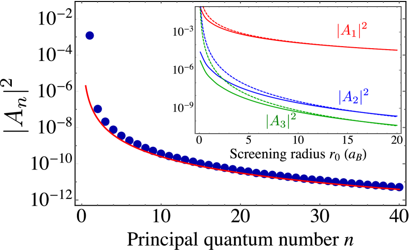
Dependence of on for is shown in Fig. 5. We see that the squared matrix element decreases rapidly with . It follows from Eq. (20) that at , therefore . Figure 5 shows that this asymptotic is valid already at .
The inset to Fig. 5 shows the dependences of the scattering probability on the screening radius . Final states with are considered. As it is mentioned above, scattering into the state for the short-range interaction is possible at only. The probability of this process decreases as , while for it drops as . The corresponding asymptotes are shown by dashed lines in Fig. 5.
C.2 Intraband Auger process
Let us now briefly address the intraband process depicted in Fig. 4(a) where the charge carriers remain in the same bands after the scattering. For free carriers the process has a high threshold requiring the initial and final wavevectors to be on the order of , otherwise the energy and momentum conservation laws cannot be satisfied simultaneously. With account for the excitonic effect the process becomes allowed because one can find, in the relative motion wavefunction Fourier image, Eq. (20), sufficiently large wavevectors due to the Coulomb interaction. In other words, the electron-hole Coulomb interaction either in the initial or in the final state may relax the momentum conservation in the course of the Auger scattering. However, the two band approximation is insufficient to give a correct result, since (i) the model approximations for the band dispersions are, as a rule, invalid at the kinetic energies due to the interaction with remote bands abakumov_perel_yassievich ; Kormanyos:2015a and (ii) the asymptotic form of at large wavevectors can strongly differ from a simplified hydrogenic model (20) birpikus_eng ; Qiu:2013a ; Wang:2017b . Thus, we present here only analytical estimations based on the parabolic approximations for the band dispersions and assuming that the ratio is very large, which allows to take into account the Coulomb effects perturbatively.
We start from the direct process. Instead of Eq. (14) we have for the free carrier scattering
| (22) |
As compared with Eq. (14) the factor is absent due to the fact that only one charge carrier changes the band. Making use of the following notations
| (23) | |||
we obtain for the exciton Auger scattering matrix element the following expression
| (24) |
Here we take into account that only excitons with positive energies of relative motion can be in the final state, i.e., corresponds to the continuum electron-hole pair state modified by the Coulomb interaction. The final state wavevector can be estimated from the energy conservation condition with the result . In this estimate we neglected thermal energy of excitons as compared with and, as before, took the same effective masses for an electron and a hole.
Since the integral in Eq. (24) can be evaluated decomposing the exponent in the series. At the integral in Eq. (24) equals to zero due to orthogonality of the functions of discrete and continuous spectra. Therefore we take into account the -linear term:
| (25) |
where
| (26) |
Within the hydrogenic model, which is used hereafter for crude estimations, and the ratio of the interband contribution (15) and the intraband contribution (24) can be estimated as
| (27) |
Thus, the resonant interband process is dominant. Similar estimate holds for the exchange contributions.
C.3 Auger recombination rate
The exciton Auger recombination rate at resonant interband scattering of two excitons into the exciton state is given by [cf. Eq. (3) of the main text]
| (28) |
In order to calculate the rate of transitions we take into account that the matrix element depends on the principal quantum number of the final state and is independent of the initial wavevectors of excitons.
Let us first assume that there is exact resonance, i.e., for the certain value of at we have
| (29) |
where is the binding energy of state. Removing the energy conservation -function and assuming that
| (30) |
i.e., the excitons are distributed according to the Boltzmann law at the temperature , is the normalization constant determined from the condition
where the factor accounts for the spin and valley degeneracy, we have
| (31) |
Note, that the Auger process is active for collisions of bright (spin-allowed) excitons with bright or dark ones, while for the dark-dark scattering the process is strongly suppressed. In the latter case the admixture with the valence band is minor and the recombination via discussed channel is not effective. The Auger decay rate can be recast in the alternative form
| (32) |
where we introduced the Auger recombination time . Since , we have an estimate in the case of the resonance with state
| (33) |
where is the lattice constant. At K, Å, nm, eV, and the exciton density cm-2 this estimate yields ps.
Let us now take into account the detuning
| (34) |
We have the sum over in the following form:
| (35) |
We see that the difference with the case of zero detuning is the exponent. The Auger recombination rate is given by
| (36) |
References
- (1) Novoselov, K. S., Mishchenko, A., Carvalho, A. & Castro Neto, A. H. 2d materials and van der waals heterostructures. Science 353 (2016).
- (2) Geim, A. K. & Grigorieva, I. V. Van der waals heterostructures. Nature 499, 419—425 (2013).
- (3) Mak, K. F., Lee, C., Hone, J., Shan, J. & Heinz, T. F. Atomically thin : A new direct-gap semiconductor. Phys. Rev. Lett. 105, 136805 (2010).
- (4) Splendiani, A. et al. Emerging photoluminescence in monolayer mos2. Nano Letters 10, 1271 (2010).
- (5) Wang, Q. H., Kalantar-Zadeh, K., Kis, A., Coleman, J. N. & Strano, M. S. Electronics and optoelectronics of two-dimensional transition metal dichalcogenides. Nature nanotechnology 7, 699–712 (2012).
- (6) Mak, K. F. & Shan, J. Photonics and optoelectronics of 2d semiconductor transition metal dichalcogenides. Nature Photonics 10, 216–226 (2016).
- (7) Wang, G. et al. Colloquium: Excitons in atomically thin transition metal dichalcogenides. Rev. Mod. Phys. 90, 021001 (2018).
- (8) He, K. et al. Tightly bound excitons in monolayer . Phys. Rev. Lett. 113, 026803 (2014).
- (9) Ugeda, M. M. et al. Observation of giant bandgap renormalization and excitonic effects in a monolayer transition metal dichalcogenide semiconductor. Nature Materials 13, 1091–1095 (2014).
- (10) Chernikov, A. et al. Exciton binding energy and nonhydrogenic rydberg series in monolayer . Phys. Rev. Lett. 113, 076802 (2014).
- (11) Ye, Z. et al. Probing Excitonic Dark States in Single-layer Tungsten Disulfide. Nature 513, 214–218 (2014).
- (12) Qiu, D. Y., da Jornada, F. H. & Louie, S. G. Optical spectrum of mos2: Many-body effects and diversity of exciton states. Phys. Rev. Lett. 111, 216805 (2013).
- (13) Ramasubramaniam, A. Large excitonic effects in monolayers of molybdenum and tungsten dichalcogenides. Phys. Rev. B 86, 115409 (2012).
- (14) Wang, G. et al. Giant enhancement of the optical second-harmonic emission of monolayers by laser excitation at exciton resonances. Phys. Rev. Lett. 114, 097403 (2015).
- (15) Jin, C. et al. Interlayer electron-phonon coupling in wse2/hbn heterostructures. Nature Physics (2016).
- (16) Manca, M. et al. Enabling valley selective exciton scattering in monolayer wse2 through upconversion. Nature communications 8, 14927 (2017).
- (17) Chow, C. M. E. et al. Unusual exciton-phonon interactions at van der waals engineered interfaces. Nano Letters (2017).
- (18) Cadiz, F. et al. Excitonic linewidth approaching the homogeneous limit in -based van der waals heterostructures. Phys. Rev. X 7, 021026 (2017).
- (19) Ajayi, O. A. et al. Approaching the intrinsic photoluminescence linewidth in transition metal dichalcogenide monolayers. 2D Materials 4, 031011 (2017).
- (20) Wang, Z., Shan, J. & Mak, K. F. Valley-and spin-polarized landau levels in monolayer wse2. Nature Nanotechnology (2016).
- (21) Wierzbowski, J. et al. Direct exciton emission from atomically thin transition metal dichalcogenide heterostructures near the lifetime limit. Scientific reports 7, 12383 (2017).
- (22) Robert, C. et al. Optical spectroscopy of excited exciton states in monolayers in van der waals heterostructures. Phys. Rev. Materials 2, 011001 (2018).
- (23) Seidel, W., Titkov, A., André, J. P., Voisin, P. & Voos, M. High-efficiency energy up-conversion by an ”auger fountain” at an inp-aiinas type-ii heterojunction. Phys. Rev. Lett. 73, 2356–2359 (1994).
- (24) Hellmann, R. et al. Low-temperature anti-stokes luminescence mediated by disorder in semiconductor quantum-well structures. Phys. Rev. B 51, 18053–18056 (1995).
- (25) Poles, E., Selmarten, D. C., Mićić, O. I. & Nozik, A. J. Anti-stokes photoluminescence in colloidal semiconductor quantum dots. Applied Physics Letters 75, 971–973 (1999).
- (26) Paskov, P. P. et al. Photoluminescence up-conversion in inas/gaas self-assembled quantum dots. Applied Physics Letters 77, 812–814 (2000).
- (27) Chen, S. L. et al. Efficient upconversion of photoluminescence via two-photon absorption in bulk and nanorod zno. Applied Physics B 108, 919–924 (2012).
- (28) Jones, A. M. et al. Excitonic luminescence upconversion in a two-dimensional semiconductor. Nature Physics (2015).
- (29) Kormanyos, A. et al. k.p theory for two-dimensional transition metal dichalcogenide semiconductors. 2D Materials 2, 022001 (2015).
- (30) Kavoulakis, G. M. & Baym, G. Auger decay of degenerate and bose-condensed excitons in o. Phys. Rev. B 54, 16625–16636 (1996).
- (31) Wang, F., Wu, Y., Hybertsen, M. S. & Heinz, T. F. Auger recombination of excitons in one-dimensional systems. Phys. Rev. B 73, 245424 (2006).
- (32) Dufferwiel, S. et al. Valley-addressable polaritons in atomically thin semiconductors. Nature Photonics 11, 497 (2017).
- (33) Lundt, N. et al. Monolayered mose2: a candidate for room temperature polaritonics. 2D Materials 4, 015006 (2016).
- (34) Scuri, G. et al. Large excitonic reflectivity of monolayer encapsulated in hexagonal boron nitride. Phys. Rev. Lett. 120, 037402 (2018).
- (35) Back, P. et al. Giant paramagnetism-induced valley polarization of electrons in charge-tunable monolayer mose 2. Physical review letters 118, 237404 (2017).
- (36) Hao, K. et al. Coherent and incoherent coupling dynamics between neutral and charged excitons in monolayer mose2. Nano letters 16, 5109–5113 (2016).
- (37) Taniguchi, T. & Watanabe, K. Synthesis of high-purity boron nitride single crystals under high pressure by using ba-bn solvent. Journal of Crystal Growth 303, 525 – 529 (2007).
- (38) Wang, G. et al. Polarization and time-resolved photoluminescence spectroscopy of excitons in mose2 monolayers. Applied Physics Letters 106, 112101 (2015).
- (39) Wang, G. et al. Exciton states in monolayer mose2: impact on interband transitions. 2D Materials 2, 045005 (2015).
- (40) Ross, J. S. et al. Electrical control of neutral and charged excitons in a monolayer semiconductor. Nature communications 4, 1474 (2013).
- (41) Shree, S. et al. Exciton-phonon coupling in mose2 monolayers. arXiv preprint arXiv:1804.06340 (2018).
- (42) Glazov, M. M. et al. Intrinsic exciton-state mixing and nonlinear optical properties in transition metal dichalcogenide monolayers. Phys. Rev. B 95, 035311 (2017).
- (43) Bie, Y.-Q. et al. A mote 2-based light-emitting diode and photodetector for silicon photonic integrated circuits. Nature nanotechnology 12, 1124 (2017).
- (44) Jiang, C. et al. Zeeman splitting via spin-valley-layer coupling in bilayer mote 2. Nature communications 8, 802 (2017).
- (45) Song, S. et al. Room temperature semiconductor–metal transition of mote2 thin films engineered by strain. Nano letters 16, 188–193 (2015).
- (46) Li, Y., Duerloo, K.-A. N., Wauson, K. & Reed, E. J. Structural semiconductor-to-semimetal phase transition in two-dimensional materials induced by electrostatic gating. Nature communications 7, 10671 (2016).
- (47) Wang, Y. et al. Structural phase transition in monolayer mote 2 driven by electrostatic doping. Nature 550, 487 (2017).
- (48) Rhodes, D. et al. Engineering the structural and electronic phases of mote2 through w substitution. Nano Letters 17, 1616–1622 (2017).
- (49) Ruppert, C., Aslan, O. B. & Heinz, T. F. Optical properties and band gap of single-and few-layer mote2 crystals. Nano letters 14, 6231–6236 (2014).
- (50) Lezama, I. G. et al. Indirect-to-direct band gap crossover in few-layer mote2. Nano letters 15, 2336–2342 (2015).
- (51) Robert, C. et al. Excitonic properties of semiconducting monolayer and bilayer . Phys. Rev. B 94, 155425 (2016).
- (52) Froehlicher, G., Lorchat, E. & Berciaud, S. Direct versus indirect band gap emission and exciton-exciton annihilation in atomically thin molybdenum ditelluride . Phys. Rev. B 94, 085429 (2016).
- (53) Rytova, N. S. Screened potential of a point charge in a thin film. Proc. MSU, Phys., Astron. 3, 30 (1967).
- (54) Keldysh, L. V. Coulomb interaction in thin semiconductor and semimetal films. Soviet Journal of Experimental and Theoretical Physics Letters 29, 658 (1979).
- (55) Yang, J. et al. Robust excitons and trions in monolayer mote2. ACS nano 9, 6603–6609 (2015).
- (56) Mouri, S. et al. Nonlinear photoluminescence in atomically thin layered arising from diffusion-assisted exciton-exciton annihilation. Phys. Rev. B 90, 155449 (2014).
- (57) Kumar, N. et al. Exciton-exciton annihilation in mose2 monolayers. Phys. Rev. B 89, 125427 (2014).
- (58) Abakumov, V. N., Perel, V. I. & Yassievich, I. N. Nonradiative recombination in semiconductors (North Holland, Amsterdam, 1991).
- (59) Rybkovskiy, D. V., Gerber, I. C. & Durnev, M. V. Atomically inspired k.p approach and valley zeeman effect in transition metal dichalcogenide monolayers. Phys. Rev. B 95, 155406 (2017).
- (60) Sun, D. et al. Observation of rapid exciton-exciton annihilation in monolayer molybdenum disulfide. Nano Letters 14, 5625–5629 (2014).
- (61) Yu, Y. et al. Fundamental limits of exciton-exciton annihilation for light emission in transition metal dichalcogenide monolayers. Phys. Rev. B 93, 201111 (2016).
- (62) Yuan, L., Wang, T., Zhu, T., Zhou, M. & Huang, L. Exciton dynamics, transport, and annihilation in atomically thin two-dimensional semiconductors. The Journal of Physical Chemistry Letters 8, 3371–3379 (2017).
- (63) Hoshi, Y. et al. Suppression of exciton-exciton annihilation in tungsten disulfide monolayers encapsulated by hexagonal boron nitrides. Phys. Rev. B 95, 241403 (2017).
- (64) Robert, C. et al. Exciton radiative lifetime in transition metal dichalcogenide monolayers. Phys. Rev. B 93, 205423 (2016).
- (65) Li, Y. et al. Room-temperature continuous-wave lasing from monolayer molybdenum ditelluride integrated with a silicon nanobeam cavity. Nature nanotechnology 12, 987 (2017).
- (66) Wu, S. et al. Monolayer semiconductor nanocavity lasers with ultralow thresholds. Nature 520, 69 (2015).
- (67) Chernikov, A., Ruppert, C., Hill, H. M., Rigosi, A. F. & Heinz, T. F. Population inversion and giant bandgap renormalization in atomically thin ws 2 layers. Nature Photonics 9, 466 (2015).
- (68) Guo, H. et al. Double resonance raman modes in monolayer and few-layer . Phys. Rev. B 91, 205415 (2015).
- (69) Tonndorf, P. et al. Photoluminescence emission and raman response of monolayer mos 2, mose 2, and wse 2. Optics express 21, 4908–4916 (2013).
- (70) Carvalho, B. R., Malard, L. M., Alves, J. M., Fantini, C. & Pimenta, M. A. Symmetry-dependent exciton-phonon coupling in 2d and bulk observed by resonance raman scattering. Phys. Rev. Lett. 114, 136403 (2015).
- (71) Wang, G. et al. Double resonant raman scattering and valley coherence generation in monolayer wse. Phys. Rev. Lett. 115, 117401 (2015).
- (72) Molas, M. R., Nogajewski, K., Potemski, M. & Babiński, A. Raman scattering excitation spectroscopy of monolayer ws 2. Scientific reports 7, 5036 (2017).
- (73) Soubelet, P., Bruchhausen, A. E., Fainstein, A., Nogajewski, K. & Faugeras, C. Resonance effects in the raman scattering of monolayer and few-layer . Phys. Rev. B 93, 155407 (2016).
- (74) Stier, A. V. et al. Magnetooptics of exciton rydberg states in a monolayer semiconductor. Physical Review Letters 120, 057405 (2018).
- (75) Glazov, M. M. et al. Exciton fine structure and spin decoherence in monolayers of transition metal dichalcogenides. Phys. Rev. B 89, 201302 (2014).
- (76) Cudazzo, P., Tokatly, I. V. & Rubio, A. Dielectric screening in two-dimensional insulators: Implications for excitonic and impurity states in graphane. Phys. Rev. B 84, 085406 (2011).
- (77) Bir, G. L. & Pikus, G. E. Symmetry and Strain-induced Effects in Semiconductors (Wiley/Halsted Press, 1974).
- (78) Chao, C. Y.-P. & Chuang, S. L. Analytical and numerical solutions for a two-dimensional exciton in momentum space. Phys. Rev. B 43, 6530–6543 (1991).