Manipulation and Characterization of the Valley Polarized Topological Kink States in Graphene Based Interferometers
Abstract
Valley polarized topological kink states, existing broadly in the domain wall of hexagonal lattices systems, are identified in experiments, unfortunately, only very limited physical properties being given. Using an Aharanov-Bohm interferometer composed of domain walls in graphene systems, we study the periodical modulation of pure valley current in a large range by tuning the magnetic field or the Fermi level. For monolayer graphene device, there exists one topological kink state, and the oscillation of transmission coefficients have single period. The Berry phase and the linear dispersion relation of kink states can be extracted from the transmission data. For bilayer graphene device, there are two topological kink states with two oscillation periods. Our proposal provides an experimental feasible route to manipulate and characterize the valley polarized topological kink states in classical wave and electronic graphene-type crystalline systems.
pacs:
72.80.Vp, 72.10.-d, 73.20.AtIntroduction– Topological kink states broadly exist in the domain walls of magnetic topological insulatorsR03 ; R04 , hexagonal lattice materials, etc.R10 ; R16 ; R18 ; R13 ; R14 ; R11 ; R17 ; R19 ; R20 ; R21 ; R22 ; R08 ; R09 ; R07 ; DWs ; DWs2 ; Parittion4 ; MoS2 ; R05 ; add1 ; add2 ; add3 ; R06 ; Optic1 ; Optic2 The recent experimental observations of kink states in bilayer graphene have generate great interests in exploring the exotic properties of such states.R08 ; R09 ; R07 ; DWs ; DWs2 ; Parittion4 However, the kink states are restricted in a very narrow region, which makes it rather difficult for characterizing with common techniques, such as APRES. By now, the approaches of STM, transport and infrared measurement can only prove the existence of kink state. The pseudospin-momentum locking property, the band structure and even the number of kink states have not been determined in experiments yet. Similar problems also exist in ,MoS2 or the monolayer-graphene-like classical wave systems.R05 ; add1 ; add2 ; add3 ; R06 ; Optic2 ; Optic1
The valley polarized states can be used for fabricating valley filters, a key device for valleytronics applications.R12 ; R13 ; R21 ; R22 ; R14 ; R15 The domain walls in graphene systems, which host valley polarized topological kink states, can serve as valley filters.R21 ; R22 Nevertheless, in a single domain wall the valley current cannot be easily manipulated. Based on a current splitter composed of two crossed domain walls, the current partition rule of kink state is investigated, indicating the manipulation of valley polarized kink states through a splitter.Parittion4 ; R23 ; R24 ; Parittion3 The control of current in such a splitter is still difficult since the morphology of domain wall is unchangeable when the devices is fabricated, thus prohibit the manipulation of the kink states.
For the applications of valleytronics, the manipulation of valley polarized current conveniently is essential. Very recently, a domain network in a bilayer graphene is observed experimentally,DWs2 , which makes the interference of the kink states possible. We adopt this platform for the characterization and manipulation of kink states through quantum interference.
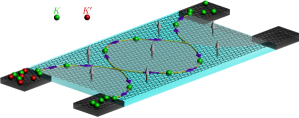
In this Letter, we study the quantum interference of the Aharanov-Bohm (AB) interferometerDWs2 ; piphase composed of topological kink states locating at the domain walls of graphene systems [see Fig.1]. Both the magnetic field and the gate voltage can be utilized to manipulate these kink states, which only allow for the valley polarized propagation and interference. The magnitude of valley polarized current can be adjusted periodically in a wide range by varying the Fermi energy or a magnetic field. The number of kink states can be obtained from the oscillation pattern of the transmission coefficients: for monolayer graphene interferometer, there is one kink state and one oscillation period; while for bilayer graphene system two kink states and two periods exist. Specifically for the former case, a Berry phase and a linear band structure of kink state can be obtained from the transport data. These exotic kink states can broadly exist in graphene-type systems including their classical wave cousins,R05 ; add1 ; add2 ; add3 ; R06 ; Optic1 ; Optic2 and thus can be realized in present experiments.
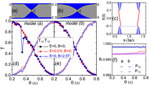
Model and methods– Four terminals graphene nanoribbon based devices with a single splitter [see Fig.2 (a) and (b)] or two splitters [see Fig.1] are investigated. Under a small voltage bias between terminal and other terminals, only electrons of valley can flow from terminal into the central region. The current is partitioned once at the splitter in devices of Fig.2 (a) and (b). In the device of Fig.1, the current is partitioned many times and the multi-beam interference happens.
The realization of monolayer graphene based domain walls is difficult in experiment. In recent works, the valley dependent transports are observed in hexagonal lattice of classical wave systems.R05 ; add1 ; add2 ; add3 ; R06 ; Optic2 The physical picture behind is the the same to the well known monolayer graphene which we will focus in the following study. In the tight-binding representation, the model Hamiltonian reads:R20 ; R22
| (1) |
with and are the creation and annihilation operators of electrons at site , respectively. The second term represents the nearest neighbor coupling with energy . The uniform perpendicular magnetic field exists only in the central region and is accounted by the phase factor . Here is the on-site energy at site to generate spatial inversion asymmetry and hence defines the domain walls.R10 ; R22 For monolayer graphene, there are two set of sublattices, namely and . In the blue (grey) region [see Fig.2 (a) and (b)], and . In the four terminals, is shifted by gate voltage away from the neutral point, which guarantees that there are dozens of states for each valley at the Fermi level.
Adopting the transfer matrix method, the transmission coefficients are calculated.Ando ; R15 Follow the standard procedure, each transmission coefficient from state in terminal to state in terminal is obtained. The valley resolved transmission coefficients are accessed by collection in two separate valleys ( and ):
| (2) |
with the Fermi energy and the magnetic field. The total transmission coefficient is and the corresponding valley polarization is . In the numerical calculation we use and with the energy unit in Eq. 1. Under the gauge transformation, the magnetic field is related to by with the C-C bond length. At zero temperature, is proportional to due to Landauer-Buttiker formula, so we only concern in the following discussion.
Single splitter– The band structure of the kink states for monolayer graphene model is displayed in Fig.2 (c). The propagation direction of the kink states at different valley is opposite to each other. First the transport of kink states in devices with a single splitter, shown in Fig. 2 (a) and (b), are investigated. Current injected from terminal , can only transmitted into terminal and . Note that in the domain wall near terminal , the current is of valley too because the energy band is reversed.R16 We find due to the valley conservation and both and are of high valley polarized [see Fig.2 (f)], signalling nearly pure valley current are obtained in the terminal and . In the following we only discuss the magnitudes of transmission coefficients. The angle dependent partition rule in Ref R23 is reproduced in Fig. 2 (d) and (e) with nonzero and . The partition of valley current is only sensitive to the intersection angle at the cross point and is independent of the Fermi level (near the neutral points), the magnetic field, or the specific line shape of the splitter.
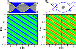
Monolayer graphene interferometer– Now we focus on interferometer formed by domain walls with two splitters as shown in Fig.3 (a). The incoming wave from terminal , at the left splitter, is partitioned to terminal and the upper arm of interferometer. At the right splitter, again the wave is split into terminal and the lower arm. Then, the wave along the lower arm meets the first splitter and is split for the third time. The process happens repeatedly and the currents flow into terminal and are the interference of multibeams. The Fermi level and magnetic field dependence of is shown in Fig.3 (c) and (d). Also due to the weak backscattering. Significantly, both and are modulated by and periodically in a wide range (e.g. and ). Note that both and are nearly valley polarized, so the device is a good controllable valley filter.
The details of are displayed in Fig.4 (a) and (b). In Fig.4 (a), two main characters are observed: i) shows a minimum at and ; ii) the oscillation of vs. is shifted periodically as changes. The magnetic flux enclosed by the interferometer [from the period of ] is about , indicating the well performance of AB interference. To better understand the characters, the redistribution of valley electrons from terminal in the interferometer is pictured by the non-equilibrium local density of states (DOS) [see Fig.4 (c-d) with the parameters marked in Fig.4 (a)]. It is calculated by with the Green’s function and the line-width function.R20 is large around the domain walls and are infinitesimal otherwise, indicating the well formation of interferometer. Moreover, in Fig.4 (c) (), there is current flows into both terminal and . In Fig.4 (d), the current flows into terminal with terminal blocked. So the interference of valley current is well tuned by the magnetic field.
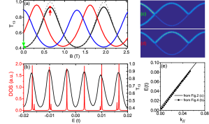
Fig.4 (b) shows the vs. relation when . varies periodically, in analogy to Fig.4 (a), indicate that the Fermi level plays a similar role as that of magnetic field, i.e. providing an extra phase. Physically the wave function is: with the momentum. When , is zero and the propagation of wave does not contribute extra phase (see Ref. Supp Fig. S1). However, when , contributes a phase to the wave function and changes the interference. Since the wave in the interferometer can only propagate clockwise, the extra phases of transmission amplitude acquired from the magnetic field and the Fermi level, are similar. To explore the peaks’ nature of , the local DOS of an isolated kink circle [the blue path in Fig.3 (b)] is shown in Fig.4 (b). The peaks’ positions of and DOS are the same. It means the peaks of are the result of resonance tunneling through the kink state circle. Interestingly, we find the zero energy is located in the middle of two peaks. It is from the Berry phase of kink state. The wave function of kink state is of two components (pseudospin), which bears the pseudospin-momentum locked topological nature.Shen After evolve along a closing circle, acquires a Berry phase.Supp Thus the Bohr-Sommerfeld quantization condition is modified to ( the circumference of the interferometer and the resonant tunneling wave vector), which means the resonant peak is not located at the zero energy. So the Berry phase can be measured from the features of . Besides, the dispersion relation of kink states can also be extracted from . For example, in Fig.4 (b), there are peaks from to and the corresponding momentum is . In Fig.4 (e), relation is shown, in good agreement with the dispersion relation adopted from Fig.2 (c).
To clarify the above characters, the scattering matrix method is adopted.MT1 ; MT2 At the left splitter, the amplitudes of the incident and outgoing waves are indicated by and , respectively [see Fig.3 (b)]. Assuming no backscattering, they are related by with the scattering matrix. In , and are the amplitudes of wave from terminal to and the upper arm of interferometer, respectively. The Berry phase effect is also accounted, e.g. from to , a Berry phase of is acquired when the momentum direction rotates an angle anticlockwise. In the right splitter, . Here is the combination of the magnetic phase and the dynamic phase. Finally, we have
| (3) |
with by using as a unit. The result is a Fabry-Pérot type interference and comes from the multi-beam interference. When , shows a maximum and shows a minimum, the same to Fig.3. For the sample size in Fig.3, , corresponds to [see Fig.2 (c)]. Substitute this value into Eq. 3 and use , the analytical results is displayed in Fig.4 (a), in good agreement with the numerical curve for . The small discrepancy at is due to the back-scattering which is omitted in the analytical approach.

Bilayer graphene interferometer– From the technique aspect, kink states interferometers in bilayer graphene are more accessible in experimental.R08 ; R09 ; R07 ; DWs ; DWs2 ; Parittion4 In the following we investigate the Bernal-stacking bilayer graphene device. The tight binding Hamiltonian is . It is constructed by the top and bottom layer of monolayer graphene (Eq.1) and the coupling in between. The spatial inversion asymmetry of bilayer graphene is induced by applying an electric field. In our model, it is accounted by the on-site energy difference between two layers. In the blue (grey) region of Fig. 5 (a), in the upper layer and in the bottom layer with . The nearest coupling between and atoms in two layers is .
Fig.5 plots the results for bilayer graphene model. In Fig.5 (c) and (d), both and vs. show periodical oscillations and the period is the same to the case for monolayer model because of the same sample size. Especially, , proportional to the pure valley current in terminal , can be tuned for 1.68/1.53 times (/). So the interference in bilayer graphene has promising application in valley current modulation as well. Different from monolayer graphene model which has only one period, in Fig.5 (c) has two periods. It is ascribed to the double kink states in bilayer model [see Fig.5 (b)]. When , the phases of two kink states are , including a same magnetic phase and non-zero dynamic phases with the momentum of two kink states (symmetric with respect to point). So and are the summation of two separate kink states’ transmission. It can be directly obtained by using the scattering method:
| (4) |
In Fig.5 (c), the fitting curves from Eq. 4 are plotted ( and ), in close agreement with the numerical results. From Eq. 4, two periods associate with are clearly seen. So far the double kink states in bilayer graphene have not yet be verified, e.g. the conductance is smaller than .R08 ; R09 Thus our proposal can provide a direct evidence to explore it. Besides, the two periods’ oscillation exists in the presence of moderate disorder (see Ref.Supp Fig.S5). So the double kink states can be confirmed in experiment more easily with our proposal, i.e. no quantized conductance required. Fig.5 (d) shows the dependence of and when . The two period feature still hold. But there exist irregular oscillation pattern which should be ascribed to the non-linear dispersion of kink states in bilayer graphene [see Fig.5 (b)]. Fig.5 (d) also demonstrate that valley current can be tuned by the Fermi level in bilayer graphene. From Eq.3 and Eq.4, the modulation of valley current is dominated by the interference phase, so above discussions hold true for interferometers of irregular shapes.DWs2
Conclusion– In conclusion, an AB interferometer is proposed to characterize and manipulate the topological valley kink states. The output of the current is perfectly valley polarized and changes periodically in a large range when sweeping the Fermi energy or the magnetic field. It provides a versatile and high efficiency way to manipulate valley degrees of freedom. For monolayer graphene, due to a single kink state, there is only one period in the transmission coefficient. The Berry phase and the linear band of kink state can be extracted from the transport measurements. However, for the bilayer graphene, there are two kink states. The transmission coefficients modulated by a magnetic flux shows two periods. Our proposal can also be used in experiments to characterize the topological nature of the kink states.
We thank the stimulus discussion with L. He and Z. W. Shi. We also acknowledge the discussion with Z. H. Hang from the experimental aspect and the related work is under processing. This work was supported by NSFC under Grants Nos. 11674264, 11534001, 11574007 and 11674028, NSF of Jiangsu Province, China (Grant No. BK20160007), National Key R and D Program of China (2017YFA0303301), NBRP of China (2015CB921102) and the Key Research Program of the Chinese Academy of Sciences (Grant No. XDPB08-4).
References
- (1) K. Yasuda, M. Mogi, R. Yoshimi, A. Tsukazaki, K. S. Takahashi, M. Kawasaki, F. Kagawa, and Y. Tokura, Quantized chiral edge conduction on domain walls of a magnetic topological insulator, Science 358, 1311 (2017).
- (2) Ilan T. Rosen, Eli J. Fox, Xufeng Kou, Lei Pan, Kang L. Wang, and David Goldhaber-Gordon, Chiral transport along magnetic domain walls in the quantum anomalous Hall effect, NPG Quantum Materials 2, 69 (2017)
- (3) G. W. Semenoff, V. Semenoff, and F. Zhou, Domain Walls in Gapped Graphene, Phys. Rev. Lett. 101, 087204 (2008).
- (4) J. Jung, F. Zhang, Z. H. Qiao, and A. H. MacDonald, Valley-Hall kink and edge states in multilayer graphene, Phys. Rev. B 84, 075418 (2011).
- (5) Abolhassan Vaezi, Yufeng Liang, Darryl H. Ngai, Li Yang, and Eun-Ah Kim, Topological Edge States at a Tilt Boundary in Gated Multilayer Graphene, Phys. Rev. X 3, 021018 (2013).
- (6) H. Pan, X. Li, F. Zhang, and S. Y. A. Yang, Perfect valley filter in a topological domain wall, Phys. Rev. B 92, 041404(R) (2015).
- (7) H. Pan, X. Li, H. Jiang, Y. G. Yao, and S. Y. A. Yang, Valley-polarized quantum anomalous Hall phase and disorder-induced valley-filtered chiral edge channels, Phys. Rev. B 91, 045404 (2015).
- (8) D. R. da Costa, Andrey Chaves, S. H. R. Sena, G. A. Farias, and F. M. Peeters, Valley filtering using electrostatic potentials in bilayer graphene, Phys. Rev. B 92, 045417 (2015).
- (9) S. G. Cheng, J. J. Zhou, H. Jiang, and Q-F. Sun, The valley filter efficiency of monolayer graphene and bilayer graphene line defect model, New J. Phys. 18, 103024 (2016).
- (10) I. Martin, Y. M. Blanter, and A. F. Morpurgo, Topological confinement in bilayer graphene, Phys. Rev. Lett. 100, 036804 (2008).
- (11) Z. H. Qiao, J. Jung, Q. Niu, and A. H. MacDonald, Electronic Highways in Bilayer Graphene, Nano Lett. 11, 3453 (2011).
- (12) F. Zhang, A. H. MacDonald, and E. J. Mele, Valley Chern numbers and boundary modes in gapped bilayer graphene, Proc. Natl Acad. Sci. USA 110, 10546 (2013).
- (13) X. Li, F. Zhang, Q. Niu, and A. H. MacDonald, Spontaneous Layer-Pseudospin Domain Walls in Bilayer Graphene, Phys. Rev. Lett. 113, 116803 (2014).
- (14) L. Ju, Z. W. Shi, N. Nair, Y. Lv, C. H. Jin, J. Velasco Jr, C. Ojeda-Aristizabal, H. A. Bechtel, M. C. Martin, A. Zettl, J. Analytis, and F. Wang, Topological valley transport at bilayer graphene domain walls, Nature 520, 650 (2015).
- (15) J. Li, K. Wang, K. J. McFaul, Z. Zern, Y. F. Ren, K. Watanabe, T. Taniguchi, Z. H. Qiao, and J. Zhu, Gate-controlled topological conducting channels in bilayer graphene, Nat. Nanotechnol. 11, 1060 (2016).
- (16) L. J. Yin, H. Jiang H, J. B. Qiao, and L. He, Direct imaging of topological edge states at a bilayer graphene domain wall, Nat. Commun. 7, 11760 (2016).
- (17) Jing Li, Rui-Xing Zhang, Zhenxi Yin, Jianxiao Zhang, Kenji Watanabe, Takashi Taniguchi, Chaoxing Liu, and Jun Zhu, A valley valve and electron beam splitter in bilayer graphene, arXiv:1708.02311
- (18) L. L. Jiang, Z. W. Shi, Bo Zeng, S. Wang, J. H. Kang, T. Joshi, C. H. Jin, L. Ju, J. Kim, T. Lyu, Y. R. Shen, M. Crommie, H. J. Gao, and F. Wang, Soliton-dependent plasmon reflection at bilayer graphene domain walls, Nature Materials, 15, 840 (2016).
- (19) L. L. Jiang, S. Wang, Z. W. Shi, C. H. Jin, M. Iqbal Bakti Utama, S. H. Zhao, Y. R. Shen, H. J. Gao, G. Y. Zhang, and F. Wang, Manipulation of domain-wall solitons in bi- and trilayer graphene, Nat. Nanotechnol. 13, 204 (2018).
- (20) A. Yan, C. S. Ong, D. Y. Qiu, C. Ophus, J. Ciston, C. Merino, S. G. Louie, and A. Zettl, Dynamics of Symmetry-Breaking Stacking Boundaries in Bilayer , J. Phys. Chem. C, 121, 22559 (2017).
- (21) J. Lu, C. Qiu, L. Ye, X. Fan, M. Ke, F. Zhang, and Z. Liu, Observation of topological valley transport of sound in sonic crystals, Nat. Phys. 13, 369 (2017).
- (22) Y. T. Yang, H. Jiang and Z. H. Hang, Topological Valley Transport in Two dimensional Honeycomb Photonic Crystals, Scientific Reports, 8, 1588 (2018).
- (23) X. X. Wu, Y. Meng, J. X. Tian, Y. Z. Huang, H. Xiang, D. Z. Han and W. J. Wen, Direct observation of valley-polarized topological edge states in designer surface plasmon crystals, Nat. Commun 8, 1304 (2017).
- (24) L. P. Ye, Y. T. Yang, Z. H. Hang, C. Y. Qiu and Z. Y. Liu, Observation of valley-selective microwave transport in photonic crystals, Appl. Phys. Lett. 111, 251107 (2017).
- (25) J. Noh, S. Huang, K. P. Chen, and M. C. Rechtsman, Observation of Photonic Topological Valley Hall Edge States, Phys. Rev. Lett. 120, 063902 (2018).
- (26) F. Gao, H.-r. Xue, Z.-j. Yang, K. Lai, Y. Yu, X. Lin, Y. Chong, G. Shvets, and B. L. Zhang, Topologically protected refraction of robust kink states in valley photonic crystals, Nat. Phys. 14, 140 (2018).
- (27) J.-W. Dong, X.-D. Chen, H. Y. Zhu, Y. Wang, and X. Zhang, Valley photonic crystals for control of spin and topology, Nat. Mater. 16, 298 (2017).
- (28) A. Rycerz, J. Tworzydlo, and C. W. J. Beenakker, Valley filter and valley valve in graphene, Nature Phys. 3, 172 (2006).
- (29) S. G. Cheng, R. Z. Zhang, J. J. Zhou, H. Jiang, and Q. F. Sun, Perfect valley filter based on a topological phase in a disordered Sb monolayer heterostructure, Phys. Rev. B 97, 085420 (2018)
- (30) Z. H. Qiao, J. Jung, C. W. Lin, Y. F. Ren, A. H. MacDonald, and Q. Niu, Current Partition at Topological Channel Intersections, Phys. Rev. Lett. 112, 206601 (2014).
- (31) K. Wang, Y. F. Ren, X. Z. Deng, S. A. Yang, J. Jung, and Z. H. Qiao, Gate-tunable current partition in graphene-based topological zero lines, Phys. Rev. B 95, 245420 (2017).
- (32) J. R. Anglin and A. Schulz, Analytical solutions of the two-dimensional Dirac equation for a topological channel intersection, Phys. Rev. B 95, 045430 (2017).
- (33) W. Chen, W.-Y. Deng, J.-Min Hou, D. N. Shi, L. Sheng, and D. Y. Xing, Spin Berry Phase in a Quantum-Spin-Hall-Insulator-Based Interferometer: Evidence for the Helical Spin Texture of the Edge States, Phys. Rev. Lett. 117, 076802 (2016).
- (34) T. Ando, Quantum point contacts in magnetic fields, Phys. Rev. B 44, 8017 (1991).
- (35) The Supplemental Material which includes other role of Fermi level (further verification), the deduction of Berry in an isolated kink state circle, the character of sample of different shape and the effect of disorder.
- (36) S.-Q. Shen, Topological Insulators, Dirac Equation in Condensed Matters, (Springer Series in Solid-State Sciences).
- (37) M. Buttiker, Y. Imry, and M. Y. Azbel, Quantum oscillations in one-dimensional normal-metal rings, Phys. Rev. A 30, 1982 (1984).
- (38) Y. Gefen, Y. Imry, and M. Y. Azbel, Quantum Oscillations and the Aharonov-Bohm Effect for Parallel Resistors, Phys. Rev. Lett. 52, 129 (1984).