Role played by strain on plasmons, screening and energy loss in graphene/substrate contacts
Abstract
The combined effect due to mechanical strain, coupling to the plasmons in a doped conducting substrate, the plasmon-phonon coupling in conjunction with the role played by encapsulation of a secondary two-dimensional (2D) layer is investigated both theoretically and numerically. The calculations are based on the random-phase approximation (RPA) for the surface response function which yields the plasmon dispersion equation that is applicable in the presence or absence of an applied uniaxial strain. We present results showing the dependence of the frequency of the charge density oscillations on the strain modulus and direction of the wave vector in the Brillouin zone. The shielding of a dilute distribution of charges as well as the rate of loss of energy for impinging charges is investigated for this hybrid layered structure.
pacs:
73.21.Ac, 71.45.-d, 71.45.Gm, 71.10.Ca, 81.05.ueI Introduction
It is undoubtedly true that there has been a tremendous effort on the part of condensed matter and materials scientists to increase their knowledge of the properties of low-dimensional structures. These include doped as well as undoped graphene,GR1 ; GR2 ; GR3 silicene,Si4 ; Si5 phosphorene,BP9 ; BP10 germanene,Ge6 ; Ge7 antimonene,Sb11 ; Sb12 tinene,Ti8 bismutheneBi13 ; Bi14 ; Bi15 ; Bi16 ; Bi17 ; Bi18 and most recently the two-dimensional pseudospin-1 latticeEjnicol . Experimental studies of such structures may involve a wide range of techniques including angle-resolved photoemission spectroscopy (ARPES)ARPES1 ; ARPES2 ; ARPES3 ; ARPES4 and electron energy loss spectroscopy (EELS)FMD2 ; Balassis ; Zaremba ; Gumbs . Both of these methods rely on an analysis of the energy of an electron emitted from or passing in the vicinity of the surface of the condensed matter under investigation. Interest in these materials stems from their potential use in device applications including transistors and state-of-the-art bismuth photonics as bismuth optical circuits have emerged as a possible replacement technology for copper-based circuits in communication and broadband networks.
We know that when an electromagnetic wave is incident on a material, especially on a conductor, the quasiparticles can respond by oscillating at specific frequencies which could be sustained over considerable distances and times if the frequency and wave number of the external perturbation are in resonance with the collective charge density oscillations. Generally, the dispersion relation of these plasmon modes is determined by the geometric and electronic properties of the 2D layer as well as the nature of the conducting substrate with which it is Coulomb coupled. In the case of free-standing graphene, the frequency of the plasmon behaves as in the long wavelength limit.Wunsch However, the plasmon dispersion relation could be modified when the two-dimensional (2D) graphene sheet is subjected to strain and also if it is coupled to the charge density oscillations and plasmons in neighboring media as illustrated in Fig. 1.
Theoretical results for EELS have been presented for free-standing graphene in Ref. [Balassis, ] where the authors reported the contributions to the rate of loss of energy due to the single-particle and plasmon excitations for particle motion parallel to the planar surface. The method of calculation was based on the formalism presented by previous authors TimTso ; Com who considered a 2D layer and cylindrical nanotube interacting with a beam of impinging charged particles. However, in recent work, Woessner, et al. Vignale ; Vignale2 released experimental and theoretical results for plasmon excitations in a heterostructure of graphene which is encapsulatedencap1 ; encap2 ; pssb between two films of hexagonal boron-nitride using a method that exploits near-field-microscopy. The collective mode spectrum revealed in the experimental data of Refs. [Vignale, ; Vignale2, ] is far more complex than that in Ref. [Balassis, ] for free-standing graphene. Consequently, we direct our attention to the heterostructure in Fig. 1 which involves atomically flat materials. Our formalism includes contributions from plasmon-phonon coupling involving transverse and longitudinal optical phonons from the surrounding conducting media. Additionally, although there have been several papers dealing with the effect due to mechanical strain on the plasmon dispersion for free standing graphene by Pelligrino et.al FMD1 , so far no consideration has been given to the influence of strain on the fast-particle energy loss spectrum or the plasmon mode dispersion for structure coomposing of a 2D layer and conducting substrate for which longitudinal and transverse phonon modes from the conducting substrate are taken into consideration.
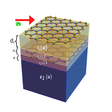
When a graphene layer is subjected to mechanical strain, the regular crystal structure is deformed which leads to a modification of its energy band structure,FMD2 ; EB1 ; EB2 ; EB3 ; EB4 ; EB5 ; Jose electrical and thermal conductivity,FMD2 ; cond1 as well as other transport properties.Trans1 ; Trans2 Meanwhile, its polarizability is altered, thereby leading to qualitative changes in the plasmon mode dispersion relation. Making use of the polarization function derived in Refs. [FMD1, ; FMD2, ; FMD3, ; FMD4, ] for strained graphene, we have investigated the plasmon mode dispersion for a structure shown schematically in Fig.1. In addition, we analyzed the effect due to strainLin on the plasmon mode dispersion relation for previously studied structuresBoperson ; Horing which are special cases of the illustrated hybrid heterostructure. We have obtained analytical and numerical results showing the effect due to strain and phonon vibrations in the substrate on the plasmon excitation spectrum in the long wavelength limit by varying several parameters including the angle giving the direction of the applied strain, the strain modulus, the separation between the graphene layers, the dielectric constant for the background material and the wave vector. This information will be useful in designing applications involving nanoelectronic and optoelectronic devices.
A critical ingredient which is needed for conducting our investigation outlined above is the surface response function. This is achieved by using a transfer matrix method, as outlined in Ref. [pssb, ], involving the electrostatic potential, electric field and the induced charge density at the interfaces of the structure shown in Fig. 1. This procedure allows us to incorporate the effect due to energy band gap, mechanical strain, as well as plasmon-phonon coupling, all of which have not been investigated simultaneously so far in our hybrid structure. Additionally, we could exploit the calculated surface response function to determine the plasmonic and single-particle excitation contributions to the rate of loss of energy for a beam of charged particles moving in the vicinity of the heterostructure.
We have organized the rest of our paper as follows: In Sec. II, we present the method for calculating the power loss of a charged particle and the introduction of the surface response function through the induced potential just outside the structure. An explicit expression for the surface response function is obtained in Sec. III by ensuring the continuity of the electrostatic potential and accounting for the change in electric field due to the induced charge density on the 2D planes where conducting carriers are located. In Sec. IV, closed-form analytic expressions are obtained in the long wavelength limit for some specific geometrical arrangements arising from Fig. 1. Detailed analytical results for the plasmon dispersion relation are presented in Sec. V for a pair of dissimilar 2D layers, with one acting as an overlayer for a dielectric in which the other is embedded. This arrangement is relevant to a recent experimental study of low frequency plasmons in a graphene-Cu(111) contact. Detailed numerical results for arbitrary wavelength are presented in Sec. VI showing the combined effect due to strain and plasmon-phonon coupling from the surrounding medium. Comparison of the energy loss from plasmons and single-particle excitations in strained and unstrained graphene is also presented. The versatility of the surface response function is further demonstrated by calculating the screened potential of an impurity located near the surface of our hybrid structure. We concluded our paper with a brief summary of our accomplishments in Sec. VII.
II Energy Loss in terms of the surface response function
We introduce our notation with a brief review. Let us assume that the medium occupies the half-space . Consider a point charge moving along a prescribed path outside the medium. The external potential satisfies Poisson’s equation which has solution
| (1) |
where with the form factor defined as
| (2) |
In this notation, is a two-dimensional wave vector in the -plane parallel to the surface which is situated at . Also, it is understood that the frequency has a small imaginary part, i.e., .
The external potential will give rise to an induced potential which, outside the structure, can be written as
| (3) |
This equation defines the surface response function . It has been implicitly assumed that the external potential is so weak that the medium responds linearly to it. The function is itself related to the density-density response function by
| (4) | |||||
which defines the induced surface charge density .
The quantity Im can be identified with the power absorption in the structure due to electron excitation induced by the external potential. The total potential in the vicinity of the surface (), is given by
| (5) |
which takes account of nonlocal screening of the external potential.
Now, let us express the induced potential as
| (6) |
Then, the instantaneous force is
| (7) | |||||
Assuming that the charge moves parallel to the surface with velocity at a height so that its trajectory is described by and . Then, in this case, the form factor in Eq. (2) becomes . Making use of this result in Eq. (7), a straightforward calculation yields the rate of loss of energy of the charged particle to the medium of plasma as
| (8) |
We can use the result in Eq. (8) to determine the contributions to from the plasmon excitations as well as the single-particle excitations for the hybrid structure shown schematically in Fig. 1. However, what is needed to proceed further with our calculation is an explicit formula for . This is achieved by making sure that the potential just outside the surface at in Eq. (5) is continuous with that inside the material and the latter is continuous throughout the region.
III Surface Response Function for a hybrid structure
The structure shown schematically in Fig. 1 consists of a graphene layer on top of a conductor with dielectric function and thickness . This in turn lies on a dielectric with background constant and thickness where another 2D layer is embedded in the middle. This whole structure is placed on a conducting substrate whose dielectric function is . We write the potential in each region with a dielectric constant displayed in Fig. 1 as
| (9) |
where are determined using the electrostatic conditions at the boundaries separating the regions.pssb After a straightforward calculation, we obtain the coefficients for the potential in the region as
| (10) |
where
| (11) |
and
| (12) |
Also,
| (13) |
with
| (14) |
and
| (15) | |||||
with
| (16) |
where the ()-dependence of the layer susceptibilities and has been suppressed for convenience. Additionally, the surface response function is expressed as:
| (17) |
with
| (18) | |||||
| (19) | |||||
we have
| (20) |
In this notation, is the permittivity of free space, for the upper 2D layer, we write for convenience and, similarly, for the lower layer, . Here, is the electron charge and, for convenience, we have introduced the polarization functions . As a matter of fact, we have
| (21) |
where is a single-particle Green’s function which is a matrix due to the underlying and sublattices.
The low-energy model Hamiltonian for unstrained graphene is well known and given by where is the Fermi velocity, in terms of Pauli matrices. When strain is applied, the low-energy Hamiltonian can be written as
| (22) |
with ,
| (23) |
and is the unit matrix, , , the carbon carbon bond length is , as the rotation matrix in the direction of the applied strain and as the angle of the applied strain with respect to the -axis, the known value for Poisson’s ratio for graphite is and for monolayer graphene it is as . The difference between the two values for the Poisson ratio is negligible compared with other parameters in our calculation. However, we chose the former value because the graphene sheet is part of a multi-layer structure. We have
| (24) |
Defining the eigenvalues and eigenvectors in the pseudospin space of the Hamiltonian without and with applied strain, as and , respectively, with as a pseudospin index, it follows that both and under applied strain are mapped onto and . The polarization function of strained graphene would then be mapped onto the polarization function of unstrained graphene by Wunsch
| (25) |
where is the polarizability of unstrained monolayer graphene. For small values of strain on graphene, the generalized polarization function FMD1 ; FMD3 may be obtained from a Taylor series expansion in and expressed approximately as
| (26) |
The subindex denotes and and the summation convention is adopted here. With the aid of the expression for the polarization of unstrained monolayer graphene in Ref. [Wunsch, ] one could proceed to calculate plasmon excitations in dimensionally mismatched Coulomb coupled 2D systems using the obtained surface response function. However, before we do so, we will examine from a numerical point of view the effect of strain on the polarization function.
Making use of the expression for the polarization function given in Eq. (26), by including or neglecting the second-order correction term, we obtain the behavior of the real part of the static polarization as shown in Fig. 2 . The upper panels of the figure show the polarizability when only the first-order correction term is included and the bottom panels correspond to the polarization when both first and second-order terms contribute. Figure 2(a) shows the polarization for three values of strain. For chosen strain, the polarization remains constant in the range . At , we see a dip due to the strain which monotonically increases afterwards. The magnitude of the polarization and the size of dip increases with increasing value of strain. Figure 2(b) in the top right panel shows the variation of polarization due to change in wave vector direction. There, we see the polarization remaining constant in the range and has the same value for any direction of the wave vector. However, the value changes when the wave vector exceeds twice the Fermi wave vector. The polarization value increases monotonically outside this range of wave vector. We could see similar behavior in the bottom panel figures when the second-order correction terms are considered. The main difference that we see there is the discontinuity at when strain is applied. This is due to the indeterminate nature of polarization at .
IV Dispersion relation for strained 2D layer-dielectric-conducting substrate heterostructure
We now turn our attention to a detailed study when a 2D layer is at a distance from a semi-infinite conducting substrate with a dielectric function with the space in between them filled with a medium of dielectric constant . For this case, we replace in Eq. (17) by , set and equal to zero. The resulting surface response function becomes
| (27) |
where
| (28) |
| (29) |
and we shall set .
At long wavelengths, we have
| (30) |
Making use of this approximation for the polarizability in Eq. (29) and then setting the resulting equation equal to zero, we obtain the dispersion equation for plasma excitations as
| (31) |
where and with , indicating the direction of the wave vector. What remains to be specified for solving Eq. (31) is the form for . In accounting for coupling between the plasmons in the 2D layer with those with frequency in the conducting substrate as well as the longitudinal and transverse optical phonons with frequency and , respectively, in this case, we have
| (32) |
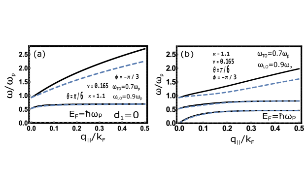
The analytic solution of Eq. (31) in conjunction with Eq. (32) for is unwieldy and is not suitable for presentation. Consequently, we present numerical results for the plasmon dispersion relations in Figs. 3(a) and 3(b) where we compare strained and unstrained graphene. In Fig. 3(a), there is no separation between the 2D layer and the surface (), whereas in Fig. 3(b), there is a separation (). This difference leads to a semi-linear plasmon branch originating from the origin in Fig. 3(b). In both panels, there is a plasmon branch close to and another near when . These two plasmon branches are a direct consequence of the plasmon-phonon interaction. Finite separation of 2D layer and the conducting substrate generates new plasmon branch from the origin called Acoustic plasmon branch. Also, for all branches in strained graphene, the slope of the uppermost dispersion curve increases the most as the strain is increased whereas, in contrast, the effect on the two other lower branches is small. This indicates how the plasmon frequency and its group velocity may be tuned for device applications.
The algebra involved in solving Eq. (31) is considerably simplified if we neglect the plasmon-phonon coupling and instead use . After a straightforward calculation, we obtain
| (33) |
where
| (34) |
| (35) |
As a special case that is of interest to experimentalists, we consider as the dielectric background which has dielectric constant, .Peeters The corresponding dispersion relations for this structure in the long wavelength limit are given by
| (36) |
and
| (37) |
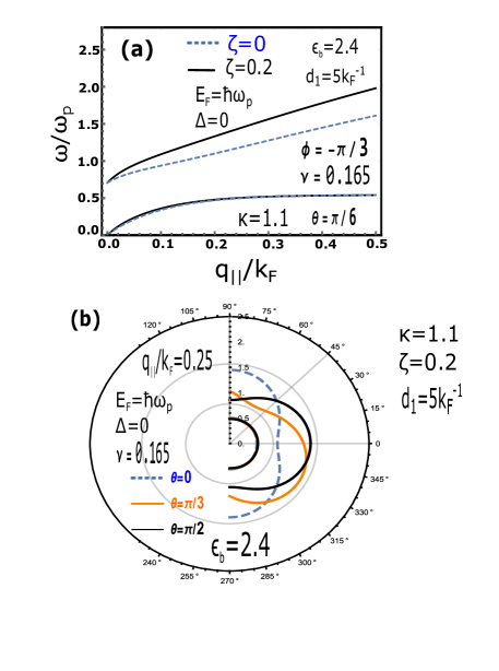
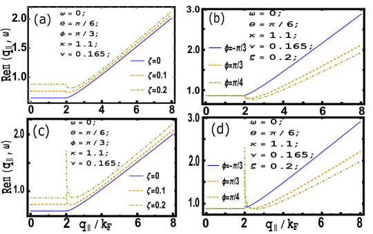
When the plasmon-phonon interaction is turned off, the spectrum of plasmon branches is changed drastically. In Fig. 4, we present results for the plasmon mode dispersion for a structure consisting of a graphene layer separated from the conducting substrate by a distance . The space in between them is filled with a dielectric having background constant , the known value for bulk graphite.Tando This separation gives rise to a linear low-frequency “acoustic” mode similar to the one in Fig. 3(b) for which there is also a spacer-layer in the structure. In Fig. 3(a), there is also a plasmon branch which is a hybrid with the surface plasmon with frequency in accordance with Eq. (36). A previous paperHoring for unstrained graphene interacting with a conducting substrate has also demonstrated the existence of two modes similar to those appearing in Fig. 4(a). However, our main goal in presenting Figs. 3 and 4 is to show the influence of strain as well as plasmon-phonon interaction for the described structure we are investigating. To present the matter in more detail, we have displayed the variation of the plasmon frequency with change in the direction of the applied strain in Fig. 4(b). The plots show that for chosen wave vector and a specified direction of the applied strain, we have two plasmon frequencies. The one with a lower frequency corresponds to acoustic plasmon whereas the higher frequency branch corresponds to hybrid plasmon mode. The plots also illustrate that the range of variation of both plasmon mode frequencies, keeping the magnitude and direction of the strain fixed and for chosen small . In Fig. 4(b), the intersection of two plasmon branches implies that for different directions of applied strain we can have the same resonating frequency for a same direction of the wave vector. We also show in Fig. 5 how the plasmon spectrum in Fig. 4 gets affected when the separation between the 2D layer and the surface reduced to zero. In any case, we still keep the interaction between the 2D layer and plasmons in the substrate. The resulting spectrum consists of only one branch originating near the surface plasmon frequency, , as is well known.Boperson The figure demonstrates the significant role in modification of the plasmon branch slope due to the application of strain although the linearity of the dispersion curve in the long wavelength limit is still preserved. We also observe only one plasmon branch which in comparison to Fig. 3(a) shows the disappearance of plasmon mode rooted from as an important effect of absence of plasmon phonon interaction.
V Plasmon excitations for a graphene-2DEG double layer
In a recent paper, Politano, et al. Politano reported some interesting results for the plasmon excitations when graphene weakly interacts with a Cu(111) substrate. Momentum-resolved electron-energy-loss spectroscopy used in their experiments revealed multiple “acoustic” surface plasmons. These authors accounted for this occurrence of low-frequency plasma modes as arising from both the graphene overlayer and the Cu(111) substrate If we follow the paper of Ahn, et al. PhysicaB and treat the Cu(111) substrate as a 2DEG, this means that we may adopt our model as follows. There is a graphene overlayer with vacuum on one side and a semi-infinite dielectric with constant on the other. We have embedded in this dielectric a 2DEG at a distance from the graphene layer. A straightforward calculation renders the surface response function for this arrangement as
| (38) |
Where , () is constant in the long wavelength limit. AS a result, one can show that the poles of the surface response function in Eq. (38) correspond to the plasmon frequencies
| (39) |
where
| (40) |
The dispersion relation in Eq. (39) is interesting and needs to be analyzed in some detail. If , as is most likely the case for a graphene-2DEG double layer, then both modes have a behavior at long wavelengths. However, if and both layers are embedded in a medium with uniform background dielectric constant, as was the case in Ref. [DasMad, ], then the frequencies are given by
| (41) |
so that one mode has a dependence while the other is linear in . All of this is incumbent on the appearance of the 2D Fourier transform of the Coulomb interaction as which appears naturally in the procedure used for calculating the surface response function. In the paper of Ahn, et al. PhysicaB , a screening parameter is introduced into the 2D Fourier transform of the Coulomb potential, which has no place in our calculations. In summary, the fundamental differences in the plasmon dispersion relations stemming from Eq. (39) arise from the nonlocal screening by the background as well as the hybridization of the underlying 2D modes.
VI Numerical Results and Discussion
VI.1 Plasma Excitations for gapless graphene
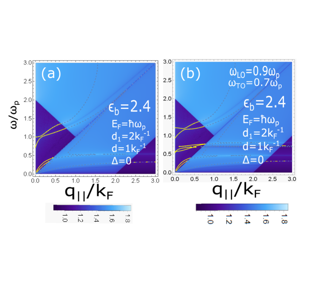
By making use of the expression for the surface response function in Eq. (17), we have carried out numerical calculations to obtain the plasmon dispersion relation for the hybrid structure shown in Fig. 1. The plasmon modes can be clearly seen in Fig. 6 where our results are presented as density plots. These results illustrate the plasmon mode for a pair of gapless graphene layers with one of them serving as a protective layer on top and the other embedded within a medium of dielectric constant . We have chosen an encapsulating dielectric material with dielectric function . The plot in the left panel of Fig. 6 shows the plasmon spectrum in the absence of phonon effects. In this case, we observe four plasmon modes in Fig. 6(a), two of which originate from the origin and are due to the 2D plasmon modes () of free-standing graphene. The remaining two have frequencies which are shifted by a depolarization from the bulk plasma frequency of the pair of encapsulating dielectric materials. However, Fig. 6(b) shows the plasmon excitations due to plasmon phonon interaction. In Fig. 6(b), we observe two additional plasmon branches along with the four plasmon modes in Fig. 6(a). These two new plasmon modes are the result of longitudinal and transverse optical phonon modes which couple with the graphene plasmon mode. In both Figs. 6(a) and (b), the plasmon modes get Landau damped as soon as they enter the single-particle excitation region(light blue). Sharp boundaries could be seen defining these regions in the figure.
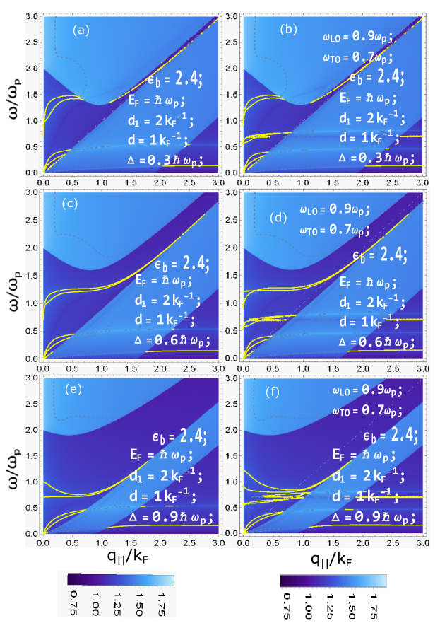
VI.2 Plasma Excitations for gapped graphene
In Fig. 7, we present our results which show the influence on the plasmon mode dispersion arising from lattice vibrations in the substrate for the structure shown in Fig. 1 when the used graphene layers have an energy band gap described by the parameter . The figures in the left panel show two pairs of plasmon modes: one pair arising from the origin and the other pair near the bulk plasmon frequency whereas the figures on the right panel show three pairs of plasmon modes. This additional pair which lies in between the other upper and lower plasmon modes is a direct result of the plasmon phonon coupling. For comparison with Fig. 6, we chose the same values of parameters for the transverse and longitudinal optical phonon frequencies and , the static background dielectric constant , the doping level as well as the thickness of the encapsulating materials. The density plots in both left and right panels show that due to the introduction of the band gap, the particle-hole excitation region splits into two parts creating a region where plasmon mode can be excited as damping- free self-sustained charge density oscillations. This region widens with the increase of the band gap leading to expanded regions for the charge density to oscillate without Landau damping. Due to increasing band gap, the members from each pair of plasmon mode group begin to merge at larger wave vector corresponding to short-range coupling.
VI.3 Plasma Excitations for strained graphene
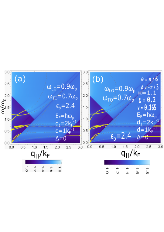
We have carried out additional calculations to examine the effect due to strain on the plasmon mode dispersion of graphene layers. In Fig. 8, we have presented our numerical results to illustrate the strain effect in the presence of plasmon phonon coupling for the given heterostructure shown in Fig. 1. The left panel of Fig. 8 shows the plasmon mode in the absence of strain whereas the right panel displays cases in the presence of strain. No great difference can be observed between these two panels because the application of a small strain does not affect the energy band structure noticeably. A small distinction between them is on the upper most pair of plasmon modes. Here, we see the two modes are not in contact with each other under no strain but they come closer under a finite strain. In a recent paper,Merano a generalization of the early surface plasmon theory [see Ref. Raether, ], was presented by including a surface currentHuang flowing within either a graphene or a Boron-Nitride monolayer on the surface of a bulk dielectric. Although the retarded interaction between the incident light and electrons in a monolayer was employed for calculating surface confinement of the TE mode of light and its propagation loss, the important nonlocal dynamics involved in optical response of electrons Iurov was neglected. Under strain, we anticipate that this mode will be affected.
VI.4 Contributions to Energy Loss
In Sec. II, we demonstrated that the power loss for a beam of charged particles moving with velocity at a distance from a surface may be expressed in terms of as given in Eq. (8). Then, subsequently, in Eq. (17), we expressed the surface response function in fractional form as . We may separate and into their real and imaginary parts so that
| (42) |
Given the form in Eq. (42), there is a contribution to the integrand in Eq. (8) whenever we have either (a) or (b) both and are simultaneously equal to zero. When case (a) holds, we have Landau damping and the particle-hole region contributes to the energy loss. In case (b), the dispersion equation for plasmon excitations is satisfied in the hybrid structure and the plasmon modes contribute. In this case, we use the Dirac identity so that
| (43) |
where the derivative here is to be evaluated at the plasmon frequency . In the case, when a graphene layer is free-standing and embedded in a dielectric medium, the power loss is simplified for a high-speed charged particle and given by
| (44) |
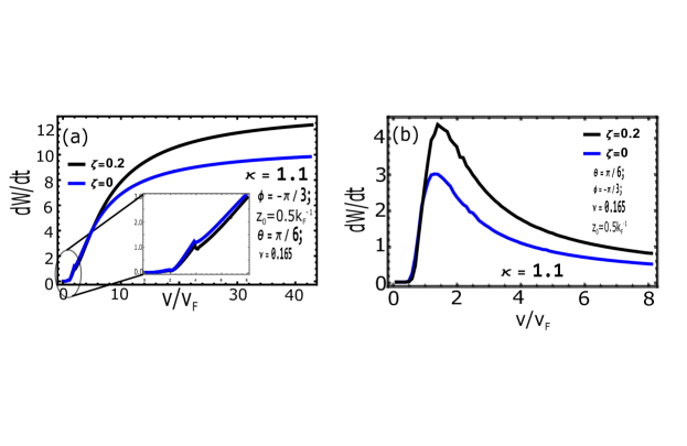
Making use of Eq.(̇8) and the surface response function in Eq. (17) for free-standing graphene, we have numerically calculated the contributions to the rate of loss of energy for a charged particle, moving parallel over the graphene sheet, due separately to single-particle excitations and the plasmon modes. Our results shown in Fig. 9 simply present the variation of the rate of loss of energy as a function of the impinging particle velocity for a chosen height . Comparison of plots for strained and unstrained graphene shows that the results are qualitatively similar over the exhibited velocity range. However, a distinct difference is observed in their magnitudes. At low velocities of a charged particle, the energy loss rates for both strained and unstrained graphene are almost equal. But, at high velocities of an incoming charged particle, the energy loss rate due to particle-holes and plasmon modes is enhanced for strained than for unstrained graphene. The energy loss rate due to particle-hole modes is increased first and eventually levels off as the value of the charged particle velocity is raised. On the other hand, the energy loss rate due to plasmon excitations for either strained or unstrained graphene remains negligible at small velocity and beyond a critical value it increases rapidly to a maximum after which it starts decreasing continuously as the particle velocity becomes larger and larger. Overall, the energy loss rate for strained graphene is greater than for unstrained graphene.
VI.5 Screened Impurity potential
Starting with Eq. (5), we obtain the static screening of the potential on the surface at due to an impurity with charge located at distance above the surface of the hybrid structure shown in Fig. 1. We have
| (45) |
By employing Eq. (45), we have computed the screened impurity potential for both strained and unstrained monolayer graphene. In Fig. 10(a), the screened potential decays exponentially with increasing height . This behavior applies for both strained and unstrained graphene. However, we note that there is a significant variation in the screened potential when the charge is put closer to the graphene sheet. In Fig. 10(b), we have calculated the screened potential as a function of the in-plane variable in units of the inverse Fermi wave number for both strained and unstrained graphene. The plot shows the occurrence of Friedel oscillations with the potential being shifted upward when strain is applied. We also notice that there is no significant change in the screened potential for strained and unstrained graphene as long as the value of is large.
VII Concluding Remarks
We have determined an expression for the rate of loss of energy for a beam of charged particles traveling parallel to the surface of a hybrid structure explicitly in terms of its surface response function. The formalism covers the case when the dependence of the response function on the in-plane wave vector is anisotropic. Specifically, we apply our formalism to investigate uniformly strained graphene both analytically and numerically. We report on the low-energy plasma excitations using an effective Dirac Hamiltonian which reveals the absence of graphene trigonal symmetry at the lowest order for weak strain. In particular, we investigate and report results for the effect due to the deformation of the Dirac cone, the band gap, doping level, thickness of the substrate, screening due to dielectric material and the effect of plasmon-phonon coupling on the plasmon modes, energy loss and static shielding of an impurity located either just outside the surface of the hybrid structure or embedded inside it. The versatility of our calculated results is that it governs an extended range of applications for investigating impurity shielding, power loss of impinging charged particles as well as the charge density oscillations for a hybrid structure such as the one depicted in Fig. 1. Strained graphene may be successfully substituted by alternative 2D materials having planar or buckled structures with lattice asymmetry. With the use of our procedure, a wide variety of stacking arrangements may also be adapted.
Acknowledgements.
D.H. would like to thank the support from the Air Force Office of Scientific Research (AFOSR). DH is also supported by the DoD Lab-University Collaborative Initiative (LUCI)Program.References
- (1) K. S. Novoselov, A. K. Geim, S.V. Morozov, D. Jiang, Y. Zhang, S. V. Dubonos, I. V. Grigorieva, and A. A. Firsov, Science 306, 666 (2004).
- (2) M. Dobbelin, A. Ciesielski, S. Haar, S. Osella, M. Bruna, A. Minoia, L. Grisanti, T. Mosciatti, F. Richard, E. A. Prasetyanto, and L. De Cola, Nature Comm. 7, 11090 (2016).
- (3) K. S. Kim, Y. Zhao, H. Jang, S. Y. Lee, J. M. Kim, K. S. Kim, J. H. Ahn, P. Kim, J. Y. Choi, and B. H. Hong, Nature 457, 706 (2009).
- (4) L. Tao, E. Cinquanta, D. Chiappe, C. Grazianetti, M. Fanciulli, M. Dubey, A. Molle, and D. Akinwande, Nature Nanotechnology 10(3), 227 (2015).
- (5) P. Vogt, P. De Padova, C. Quaresima, J. Avila, E. Frantzeskakis, M. C. Asensio, A. Resta, B. Ealet, and G. Le Lay, Phys. Rev. Lett. 108 155501 (2012).
- (6) L. Li, Y. Yu, G. J. Ye, Q. Ge, X. Ou, H. Wu, D. Feng, X. H. Chen, and Y. Zhang. Nature Nano., 9, 372 (2014).
- (7) P. Yasaei, B. Kumar, T. Foroozan, C. Wang, M. Asadi, D. Tuschel, J. E. Indacochea, R. F. Klie, and A. Salehi-Khojin. Advanced Materials 27, 1887 (2015).
- (8) L. Li, S. Z. Lu, J. Pan, Z. Qin, Y. Q. Wang, Y. Wang, G. Y. Cao, S. Du, and H. J. Gao, Advanced Materials 26(28), 4820 (2014).
- (9) M. Derivaz, D. Dentel, R. Stephan, M. C. Hanf, A. Mehdaoui, P. Sonnet, and C. Pirri, Nano lett. 15, 2510 (2015).
- (10) J. Ji, X. Song, J. Liu, Z. Yan, C. Huo, S. Zhang, M. Su, L. Liao, W. Wang, Z. Ni, and Y. Hao, Nature Comm. 7, 13352 (2016).
- (11) P. Ares, F. Aguilar-Galindo, D. Rodr guez-San-Miguel, D. A. Aldave, S. D az-Tendero, M. Alcam , F. Mart n, J. G mez-Herrero, and F. Zamora, Advanced Materials 28(30), 6332 (2016).
- (12) F. F. Zhu, W. J. Chen, Y. Xu, C. L. Gao, D. D. Guan, C. H. Liu, D. Qian, S. C. Zhang, and J. F. Jia. Nature Materials 14(10), 1020 (2015).
- (13) T. Hirahara, T. Nagao, I. Matsuda, G. Bihlmayer, E.V. Chulkov, Y.M. Koroteev, P.M. Echenique, M. Saito, and S. Hasegawa, Phys. Rev. Lett. 97(14), 146803 (2006).
- (14) T. Hirahara, T. Shirai, T. Hajiri, M. Matsunami, K. Tanaka, S. Kimura, S. Hasegawa, and K Kobayashi, Phys. Rev. Lett. 115(10), 106803 (2015).
- (15) T. Hirahara, N. Fukui, T. Shirasawa, M. Yamada, M. Aitani, H. Miyazaki, M. Matsunami, S. Kimura, T. Takahashi, S. Hasegawa, and K. Kobayashi, Phys. Rev. Lett. 109, 227401 (2012).
- (16) F. Yang, L. Miao, Z.F. Wang, M.Y. Yao, F. Zhu, Y.R. Song, M.X. Wang, J.P. Xu, A.V. Fedorov, Z. Sun, and G.B. Zhang, Phys. Rev. Lett. 109, 016801 (2012).
- (17) Z. F. Wang, M. Y. Yao, W. Ming, L. Miao, F. Zhu, C. Liu, C. L. Gao, D. Qian, J. F. Jia, and F. Liu. Nature Comm. 4, 1384 (2013).
- (18) C. Sabater, D. Gos lbez-Mart nez, J. Fern ndez-Rossier, J. G. Rodrigo, C. Untiedt, and J. J. Palacios, Phys. Rev. Lett. 110(17), 176802 (2013).
- (19) J. D. Malcolm, E. J. Nicol, Phys. Rev. B 93, 165433 (2016).
- (20) C. H.Park, F. Giustino, C. D. Spataru, M. L. Cohen, S. G. Louie, Nano Lett. 9, 4234 (2009).
- (21) C. Riedl, A. A. Zakharov, U. Starke, Applied Physics Lett. 93, 033106 (2008).
- (22) M. Bianchi, E. D. L. Rienks, S. Lizzit, A. Baraldi, R. Balog, L. Hornek r, P. Hofmann, Phys. Rev. B 81, 041403 (2010).
- (23) M. Kralj, I. Pletikosic, M. Petrovic, P. Pervan, M. Milun, C. Busse, T. Michely, J. Fujii, and I. Vobornik, Phys. Rev. B84, 075427 (2011).
- (24) F. M. D. Pellegrino, G. G. N. Angilella, R. Pucci, Phys. Rev. B 81, 035411 (2010).
- (25) V. Fessatidis, N. J. M. Horing, and A. Balassis, Physics Letters 375, 192 (2010).
- (26) B. N. J. Persson, and E. Zaremba, Phys. Rev. B 31, 1863 (1985).
- (27) G. Gumbs, Phys. Rev. B 39, 5186 (1989).
- (28) B. Wunsch, T. Stauber, F. Sols, and F. Guinea, New Journal of Physics 8, 318 (2006).
- (29) N. J. M. Horing, H. C. Tso, G. Gumbs, Phys. Rev. B 36, 1588 (1987).
- (30) G. Gumbs, and A. Balassis, Phys. Rev. B71, 235410 (2006).
- (31) A. Woessner, M. B. Lundeberg, Y. Gao, A. Principi, P. A. Gonz lez, M. Carrega, K. Watanabe, T. Taniguchi, G. Vignale, M. Polini, and J. Hone, Nature Materials 14, 421 (2015).
- (32) A. Principi, M. Carrega, M. B. Lundeberg, A. Woessner, F. H. Koppens, G. Vignale, and M. Polini, Phys. Rev. B 90, 165408 (2014).
- (33) G. Gumbs, N. J. Horing, A. Iurov, and D. Dahal, Journal of Physics D: Applied Physics 49, 225101 (2016).
- (34) S. M. Badalyan and F. M. Peeters, Phys. Rev. B 85, 195444 (2012).
- (35) G. Gumbs, D. Dahal, and A. Balassis, Physica Status Solidi (b) 255, 1700342 (2018).
- (36) F. M. D. Pellegrino, G. G. N. Angilella, and R. Pucci, Phys. Rev. B 82, 115434 (2010).
- (37) C. Bena, Phys. Rev. B 79, 125427 (2009).
- (38) F. M. Pellegrino, G. G. N. Angilella, and R. Pucci, Phys. Rev. B 80, 094203 (2009).
- (39) M. Farjam, and H. Rafii-Tabar, Phys. Rev. B 80, 167401 (2009).
- (40) G. Gui, J. Li, and J. Zhong, Phys. Rev. B 78, 075435 (2008).
- (41) V. M. Pereira, A. C. Neto, and N. M. R. Peres, Phys. Rev. B 80, 045401 (2009).
- (42) M. O. Leyva, and C. Wang, Journal of Physics: Condensed Matter 29(16), 165301 (2017).
- (43) V. M. Pereira, R. M. Ribeiro, N. M. R. Peres, A. C. Neto, Europhysics Letters 92, 67001 (2011).
- (44) F. M. D. Pellegrino, G. G. N. Angilella, and R. Pucci, Phys. Rev. B 84, 195404 (2011).
- (45) D. Dahal, and G. Gumbs, Journal of Physics and Chemistry of Solids 100, 83-91 (2017).
- (46) F. M. D. Pellegrino, G. G. N. Angilella, and R. Pucci. Phys. Rev. B 84, 195407 (2011).
- (47) F. M. D. Pellegrino, G. G. N. Angilella, and R. Pucci. Phys. Rev. B 84, 195404 (2011).
- (48) J. H. Wong, B. R. Wu, and M. F. Lin, Journ. of Phys. Chem. C 116, 8271 (2012).
- (49) B. N. J. Persson, Solid State Commun. 52, 811 (1984).
- (50) G. Gumbs, A. Iurov, and N. J. M. Horing, Phys. Rev. B 91, 235416 (2015).
- (51) S. M. Badalyan and F. M. Peeters, Phys. Rev. B 85, 195444 (2012).
- (52) T. Ando, Jour. Physical Soc. Jap. 75, 074716 (2006).
- (53) A. Politano, H. K. Yu, D. Far as, and G. Chiarello, Phys. Rev. B 97, 035414 (2018).
- (54) J. K. Ahn, Y. I. Kim, K. H. Kim, C. J. Kang, M. C. Ri, and S. H. Kim, Physica B: Condensed Matter 481, 257 (2016).
- (55) S. Das Sarma and A. Madhukar, Phys. Rev. B 23, 805 (1981).
- (56) M. Merano, Optics letters 41(11), 2668-2671 (2016).
- (57) H. Raether, Springer 111, 91(1988).
- (58) D. Huang, C. Rhodes, P. M. Alsing, and D. A. Cardimona, J. Appl. Phys. 100, 113711 (2006).
- (59) A. Iurov, D. Huang, G. Gumbs, W. Pan, and A. A. Maradudin, Phys. Rev B 96, 081408(R) (2017).