Are slot and sub-wavelength grating waveguides better than strip waveguides for sensing?
Abstract
The unique ability of slot and sub-wavelength grating (SWG) waveguides to confine light outside of the waveguide core material has attracted significant interest in their application to chemical and biological sensing. However, high sensitivity to sidewall roughness induced scattering loss in these structures compared to strip waveguides casts doubt on their efficacy. In this article, we seek to settle the controversy for silicon-on-insulator (SOI) photonic devices by quantitatively comparing the sensing performance of various waveguide geometries through figures of merit that we derive for each mode of sensing. These methods (which may be readily applied to other material systems) take into account both modal confinement and roughness scattering loss, the latter of which is computed using a volume-current (Green’s-function) method with a first Born approximation. For devices based on the standard 220 nm SOI platform at telecommunication wavelengths ( nm) whose propagation loss is predominantly limited by random line-edge sidewall roughness scattering, our model predicts that properly engineered TM-polarized strip waveguides claim the best performance for refractometry and absorption spectroscopy, while optimized slot waveguides demonstrate performance enhancement over the other waveguide geometries for waveguide-enhanced Raman spectroscopy.
1 Introduction
Waveguide based chemical and biological sensing is rapidly advancing as a prime application area for integrated photonics. However, there is currently no universally agreed-upon waveguide geometry that optimally enhances detected signals in the presence of fabrication-induced scattering losses. In classical strip waveguide sensors (Fig. 1), molecules of interest interact with the relatively weak evanescent electric field outside the waveguide core. To boost light–molecule interactions, slot waveguides [1, 2, 3, 4, 5, 6] and SWG waveguides [7, 8, 9] have been proposed and demonstrated as alternative sensing platforms. In these waveguides, a larger fraction of the mode resides in the low-index cladding (usually the sensing medium, such as air or water) where the molecules are located. Indeed, improved refractive-index sensitivity (defined as the induced wavelength detuning per unit refractive-index change in the surrounding media) has been experimentally validated in resonator refractometry sensors based on both slot and SWG waveguides [1, 2, 8], and enhanced Raman conversion efficiency per unit device length has also been measured in slot waveguides [10]. Nevertheless, the benefits may be offset by their increased susceptibility to optical loss induced by sidewall-roughness scattering. Many authors have studied roughness loss in dielectric waveguides both theoretically (through coupled-mode theory and the volume-current / Green’s-function methods [11, 12, 13, 14]) and experimentally [15, 16, 17, 18], but these analyses focused only on minimizing the power scattered into the far field. This tradeoff between mode confinement and attenuation is typically reported for plasmonic waveguide structures [19, 20, 21, 22, 23, 24] and some resonant sensor devices [25, 26, 27, 28], but differences in fabrication conditions often make it difficult to perform side-by-side comparisons. Efficiently quantifying the tradeoff between mode delocalization and scattering loss is critically important for the rational design of chip-scale photonic sensors (as well as electro-optic modulators [29] and light sources [30]) and to date there seems to be no work that quantifies these two effects with a single figure of merit (FOM) for strip, slot, and SWG waveguides.
In this paper, we develop easily computed figures of merit (Sec. 2) that capture the precise trade-off between field confinement and roughness-induced scattering loss for waveguide-based sensing applications. The key to efficiently evaluating our figures of merit is perturbation theory [12, 31], both to evaluate the impact of mode confinement on sensing (see Sec. 2 and Supplemental Information (SI)) and also to evaluate roughness scattering by computing the power radiated by equivalent current sources along the surface [14, 32] (Sec. 3). The latter approach circumvents costly and roughness-dependent direct simulation of disordered waveguides, giving us a figure of merit comparison independent of the precise roughness statistics as long as the roughness correlation length is sub-wavelength. Although computation of the “effective” sources to represent roughness scattering is in general quite complicated [14], we both propose a powerful general approach and we demonstrate that, for typical experimental roughness, a simple “locally flat perturbation” approximation is accurate (Sec. 3 and SI). The results of this work indicate that larger modal overlap with the sensing medium does not always correspond to better performance (due to increased scattering losses). By evaluating our figures of merit for strip, slot, and sub-wavelength grating (SWG) designs for bulk/surface/Raman sensing (Sec. 4), we obtain the results that for typical SOI waveguides at a wavelength of =1550 nm (1) the simple TM-polarized strip waveguide is better than other geometries considered here for bulk absorption sensing and refractometry, (2) the TM-polarized strip waveguide and TE-polarized slot waveguide are both better than other geometries for surface-sensitive refractometry and absorption sensing, and (3) the TE-polarized slot waveguide is better than other geometries for Raman sensing. Furthermore, we provide an extensive comparison (Sec. 5) to published experimental results, in which we applied our numerical method to compute the ratio of losses for pairs of waveguide geometries that were fabricated and reported in the literature, and our predictions exhibit good agreement to within experimental accuracy. As discussed in our concluding remarks (Sec. 6), we believe that these comparisons and figures of merit will drive future experimental and theoretical exploration of new waveguide geometries for the purpose of sensing.
2 Sensing Figures of Merit
Here we consider three sensing techniques: 1) surface-sensitive refractometry and absorption sensing, where a sensor surface is coated with a binding agent (e.g. antibody) that specifically attaches to the target molecule and the device monitors the change in index or optical absorption caused by monolayer or few-layer molecular binding on the surface; 2) bulk index/absorption sensing, where the sensor detects the change in bulk index/absorption in the adjacent sensing medium; and 3) waveguide-enhanced Raman spectroscopy (WERS) [33, 34, 35], where the excitation light and spontaneous Raman emission signal from molecules in the surroundings co-propagate in a waveguide. In all cases, the sensor performance is related to the external confinement factor and divided by the attenuation coefficient. This “benefit-to-cost” ratio is described in [28] for absorption spectroscopy in silicon and silicon nitride waveguides and in [19] for plasmonic waveguides, where there is a similar drive to maximize waveguide confinement and minimize the strong attenuation coefficients of surface plasmon polaritons [20]. Equivalently, for optical resonator refractometers the appropriate figure of merit is often stated as the ratio of the refractive-index sensitivity to the resonance full-width at half maximum (FWHM) (which is proportional to the attenuation coefficient) [25, 26, 21, 27, 22, 23, 24]. For most prior literature that analyzes sensing in non-resonant waveguide devices (and also some resonant devices [36, 2, 37]), the quantity of interest typically reported is the fractional power change for a small increase in analyte (i.e. the numerator of our FOM) [38, 39, 5, 40, 41, 42, 43]. This is likely due to the difficulty in precisely measuring the attenuation coefficient or scattering loss for a single evanescent waveguide sensor or Mach–Zehnder refractometer [15, 44] (in contrast, for resonant devices this information is immediately available in the resonance FWHM) [45].
The general goal in the first two sensing modes is to maximize the device sensitivity, which is the change in fractional optical power () induced by a small change in the number of analyte molecules that alter the cladding absorption coefficient or index of refraction. Thus, the relevant metric is the sensitivity in units of inverse number density. For example, as described in the SI, the absorption sensitivity is proportional to , where is either the external confinement factor of the entire cladding region for bulk sensing or the surface region (approximated by a thin volume next to the interface), is the scattering loss per unit length, and is the molecular absorption coefficient (related to the bulk absorption coefficient via , where is the number density of analyte molecules). In general, we find that the only geometry dependence occurs in a factor , leading us to the dimensionless figure of merit for surface sensitive and bulk absorption/index sensing:
| (1) |
where is the vacuum wavelength of light. In the third sensing mode (Raman sensing), the goal is to maximize the power of Raman scattered light collected at the output of a waveguide for a given input laser power. As such, the corresponding figure of merit is the dimensionless quantity derived in the SI:
| (2) |
where is the Raman gain coefficient (with units of 1/length) defined as the power of evanescently scattered Raman light collected back into the waveguide per unit length and normalized by the input power. The external confinement factor [46, 47, 48, 49, 50, 51, 52, 53] as well as the Raman gain coefficient are quantified via perturbation theory (see SI):
| (3) | ||||
| (4) |
where , , and are the cladding material, effective, and waveguide group indices, is the permittivity, is the electric field of the waveguide mode, is the input angular frequency, integration is over the cross section of the waveguide, restricted in the numerator to the cladding/sensing region, and is the speed of light. We also assume that the Raman shift is relatively small so that . For periodic structures such as SWG waveguides, integration is performed over the volume of a unit cell with period :
| (5) |
We note here that the optimized length of the waveguide for is and for is . In this work we assume that sidewall roughness scattering constitutes the dominant source of optical loss in waveguides, which is typically the case in high-index-contrast waveguide systems at moderate optical powers such as SOI [54, 55, 56], silicon nitride on insulator [57, 58], chalcogenide glass on oxide [59], and TiO2 on oxide [60]. We also note that each FOM is generic to many different sensing device configurations, such as serpentine/spiral waveguides, ring resonators, and Mach–Zehnder interferometers.
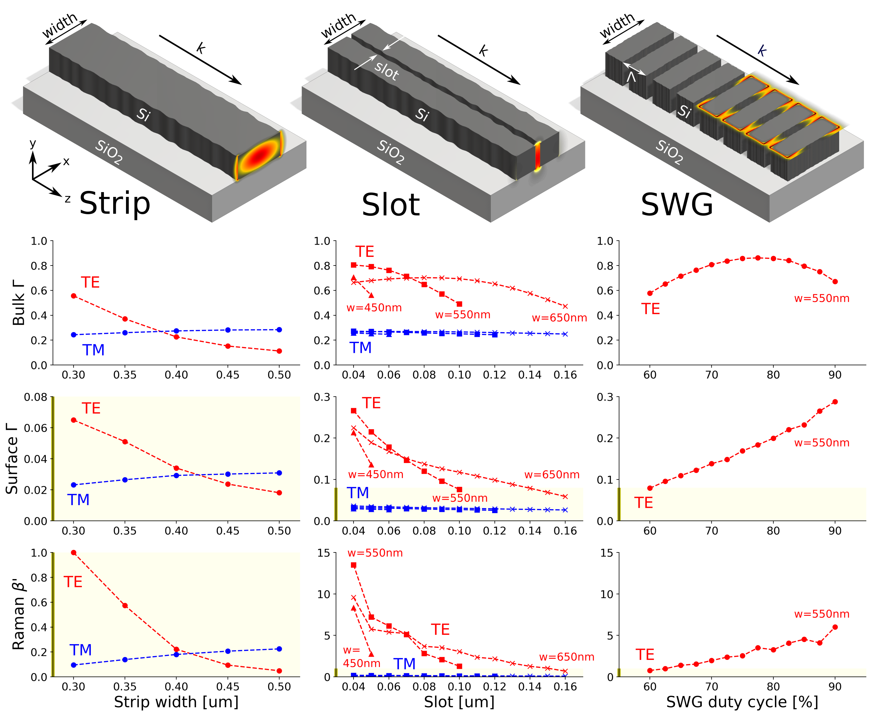
In all three cases, the sensor limit of detection (LOD) is determined by the modal overlap with the sensing region as well as the optical path length, the latter of which is limited by the waveguide propagation loss. The surface or bulk modal confinement factors and the Raman gain coefficient are readily computed from standard frequency-domain eigenmode solvers and the results are plotted in Fig. 1, which clearly show that slot and SWG structures indeed significantly enhance modal overlap with the sensing medium.
3 Scattering-loss calculations
In the volume-current method, waveguide perturbations can be described to first order (neglecting multiple-scattering effects) by dipole moments (polarizations) induced in the perturbation by the original (unperturbed) waveguide field . These perturbations act as current sources that create the scattered field. For example, a small perturbation in the permittivity acts like a current source [11, 61]. However, for perturbations in high-index-contrast waveguide interfaces, calculating the induced polarization (and hence the effective current source) is in general much more complicated [14], and requires solving a quasistatics problem (Poisson’s equation) [62]. For a given statistical distribution of the surface roughness, we show in SI how we can solve a set of quasistatics problems to compute the corresponding statistical distribution of the polarization currents. Fortunately, however, there is a simplification that applies to typical experimental regimes (, where is the correlation length of the surface roughness and the root mean square roughness amplitude). If (typically – nm for SOI waveguides) is much larger than the amplitude of the roughness (– nm in state-of-the-art devices [63, 64, 18, 65]), then one can approximate the surface perturbation as locally flat. In this case, there is an analytical formula for the induced current from a locally flat interface shifted by a distance [62]:
| (6) |
(Note that the currents depend on the orientation of relative to the interface: is the component of parallel to the surface and is the component of perpendicular to the surface.) In this case, the correlation function of the current is simply proportional to the correlation function of the surface profile. We verify in SI that the full quasistatic calculation reproduces this locally flat interface approximation in typical experimental regimes.
Given these currents and their statistical distribution (from the statistics of ), one can then perform a set of Maxwell simulations on the unperturbed waveguide geometry (hence, at moderate spatial resolution) to find the corresponding radiated power. Again, there is a somewhat complicated procedure in general to compute the effect of currents with an arbitrary correlation function. But, in the case where the correlation length ( nm) is much less than the wavelength ( m), we can approximate this “colored” noise distribution by uncorrelated “white” noise [32], effectively treating the currents as uncorrelated point sources with the same mean-squared amplitude . Since the power radiated by uncorrelated point sources is additive, we can then simply average the power radiated from different points on the surface to find the scattering loss per unit length [14]. Finally, the computation simplifies even further because we only compute the ratio of the FOMs for different waveguides, in which case all overall scaling factors and units (including all dependence on the roughness statistics and ) cancel out.
4 Comparison of Waveguide Geometries
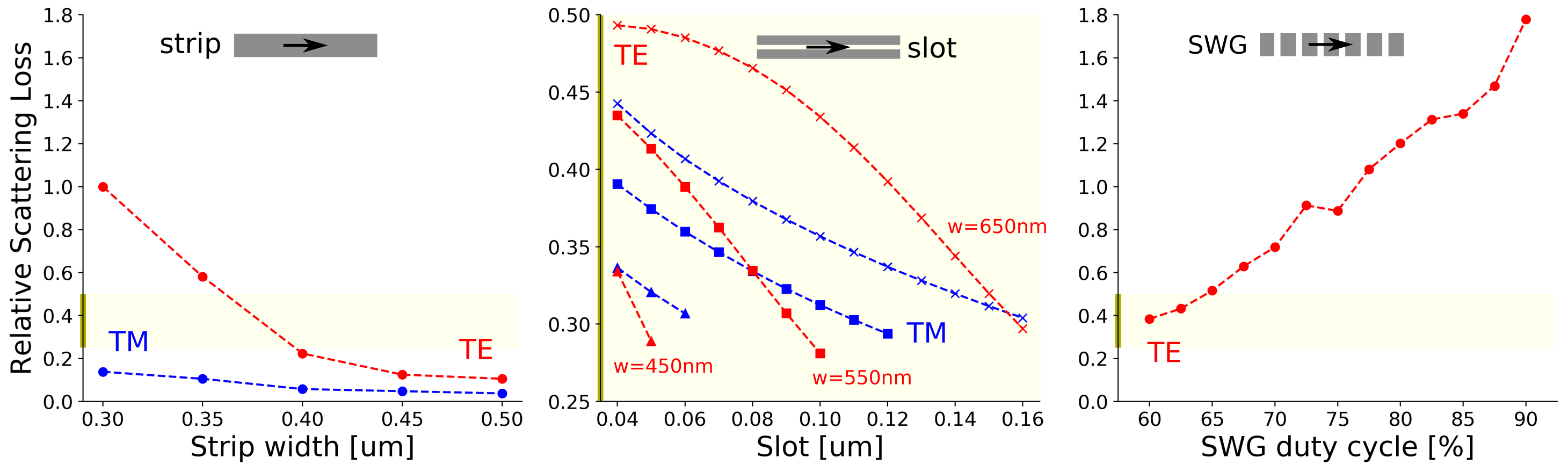
Using the aforementioned volume-current method, we quantified the relative scattering losses () for a large set of strip, slot, and SWG waveguide geometries for various design parameters such as width, slot size, and duty-cycle. All waveguide geometries (Fig. 1) are assumed to be fabricated from SOI wafers with 220 nm Si layer thickness, negligible scattering losses at the top and bottom flat surfaces, and for a target wavelength of nm. The calculations, described in detail in SI, consist of only two computationally inexpensive steps. First, we compute the electric () and displacement () field profiles using a frequency-domain eigenmode solver [31], which is used to determine the confinement factors, Raman gain coefficient, and the strength of the induced dipole moments via Eq. S37. For each unique sidewall position and for each waveguide geometry, we use a single three-dimensional finite-difference time-domain (FDTD) simulation with a vertical line of dipole moments (corresponding to vertically symmetric sidewall roughness, i.e. line-edge roughness [66, 67, 68]) to compute the scattered power from both far-field radiation and reflection. Finally, the scattered power is averaged over all inequivalent sidewall positions and computed per unit length along the direction of propagation. The relative scattering loss per unit length for the considered geometries is shown in Fig. 2.
For strip waveguides, we analyzed the TE-like and TM-like polarized modes for various waveguide widths. Results for slot waveguides of TE and TM polarization are computed for various total waveguide widths and air-slot gaps. For SWG waveguides, the width and period are fixed at 550 nm and 250 nm respectively, and only TE (-antisymmetric) modes are considered as a function of the duty cycle, which is defined by where is the grating period and is the size of the air gap along the direction. The particular width of 550 nm and polarization was chosen for this analysis since the corresponding waveguide geometries exhibit single-mode behavior for a relatively large range of duty cycles, as confirmed by numerically computed dispersion diagrams. All waveguide dimensions are chosen such that no more than one TE and one TM mode exists.
Our results indicate that slot and SWG waveguides do in fact greatly increase scattering losses relative to standard 450 nm wide TE and TM strip waveguides [69]. The scattering loss computed by the volume-current method considers both the incident field strength at the location of the perturbation and the local density of states (LDOS) [70], which is determined by the surrounding geometry. (As such, current sources at the outer edges of a strip waveguide will radiate different amounts of power than current sources in the air-gap region of a slot waveguide.) Our comparison of scattering losses for different geometries, as shown in Fig. 2, is largely consistent with prior experimentally measured values of surface roughness in SOI waveguides [71, 72, 73]. However, a direct comparison between experiment and theoretically/numerically computed values is difficult since experimental uncertainties are typically on the order of a few dB/cm. In addition, an accurate comparison of scattering losses for different geometries requires side-by-side fabrication of waveguides on the same process and material platform, since different processes introduce dramatically different roughness statistics. As such, literature for this is relatively scarce, and numerical methods provide a means for quickly evaluating and comparing new waveguide structures.
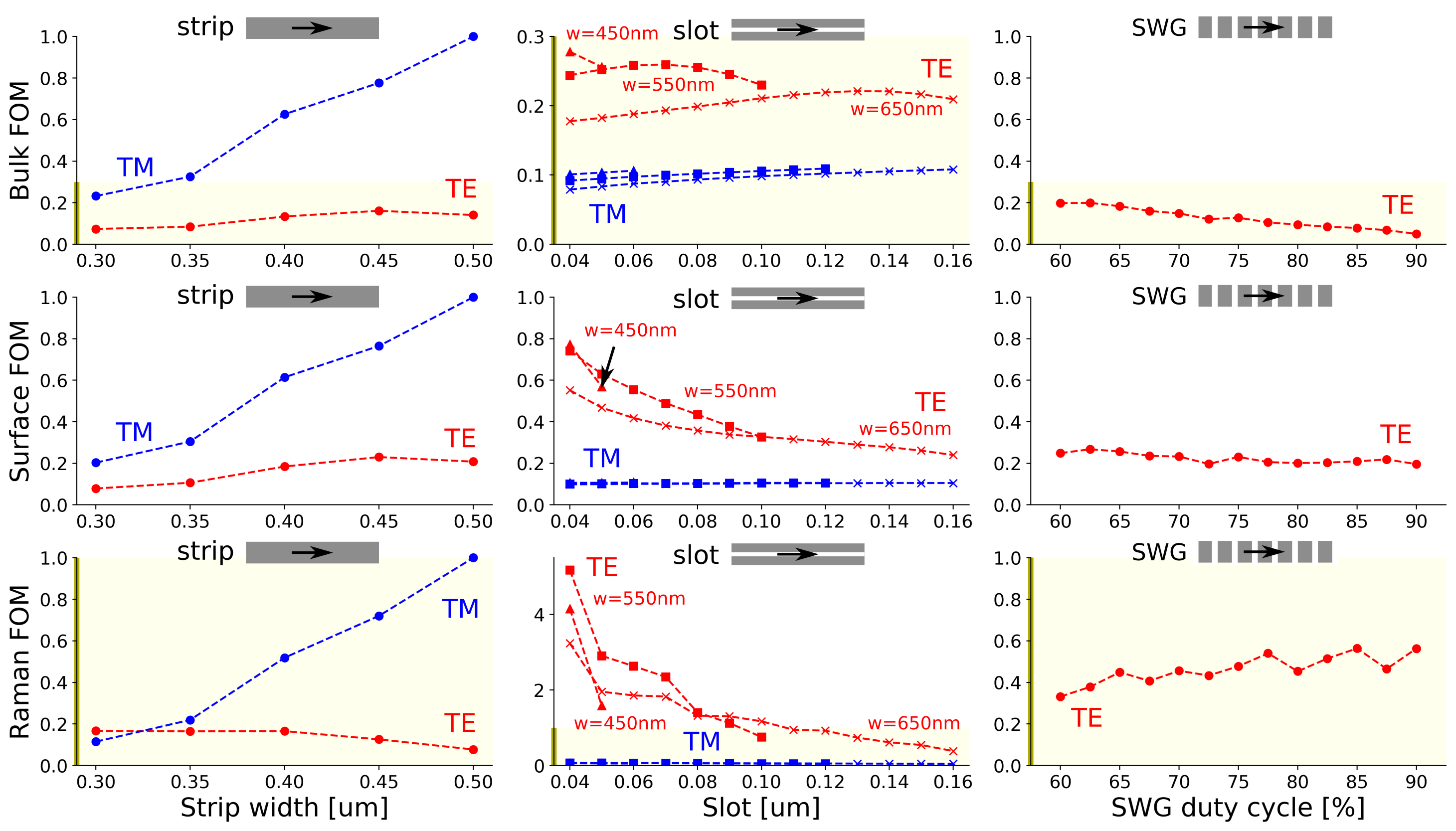
With the computed scattering losses, confinement factors, and Raman gain coefficients, we then computed the relevant FOM for each mode of sensing (via Eq. 1 and 2), which is presented in Fig. 3. Our results indicate the TE slot and SWG structures do in fact provide modest improvements in sensing performance over traditional TE-polarized strip waveguides. However, TM-polarized strip waveguides (which are here assumed to have negligible roughness on the top and bottom interfaces) exhibit significantly higher performance owing to their reduced propagation loss and longer accessible optical-path length. For bulk and surface absorption sensing, the performance of the SWG waveguides gradually decrease with increase in duty cycle (as the air-slot region becomes smaller), indicating that the increase in scattering loss in small SWG gap-regions outweighs the benefits provided by field localization in the air gap. On the other hand, slot-waveguide structures demonstrate improved performance as the slot size decreases (narrow-slot waveguides show improvement over large-slot waveguides for surface sensing and improvement for Raman sensing), with the exception of bulk absorption sensing in the air region. For bulk absorption sensing, there appears to be a critical slot size (70 nm slot for the 550 nm wide waveguides, and 130 nm slot for the 650 nm wide waveguides) below which scattering losses dominate the FOM and above which the confinement factor is suboptimal.
For Raman spectroscopy, the gain coefficient is related to the fourth power of electric field rather than the square of the electric field, so regions of high electric field exhibit significant performance enhancements, as shown by the numerically computed values of the relative Raman gain coefficient in Fig. 1. In our computations, we find that waveguides with narrow slots do in fact tend to produce sufficiently more Raman signal than what is lost due to sidewall scattering at the silicon/air interface. Wide (550 nm) silicon waveguides with narrow (40 nm) air slots yield the highest bulk Raman FOM by a factor of over SWG waveguides and over TM strip waveguide modes. Despite having an improved Raman gain coefficient, the SWG structures suffer from significantly higher scattering losses due to the increased sidewall surface area.
5 Comparison with experiment
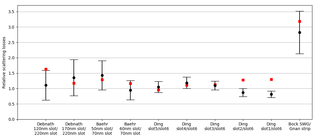
In order to demonstrate the utility and accuracy of this approach, we searched the literature for reports of fabricated strip, slot, and sub-wavelength grating silicon waveguides and their associated propagation losses [73, 74, 75, 76, 77]. We then applied the volume-current method to compute the relative scattering losses for each of 14 reported waveguide geometries. Since the waveguides of different geometries reported within each manuscript are fabricated using identical processing protocols which presumably result in identical or similar roughness characteristics, the reported losses are expected to accurately correspond to the different waveguide geometries. The authors in Bock et al. [76] only report the loss for a single SWG structure and reference Gnan et al. [77] to compare with strip waveguide losses. Both reported devices were fabricated using similar fabrication protocols (electron-beam lithography with hydrogen silsesquioxane resist and reactive-ion etching), and so we show in Fig. 4 the ratio of the reported propagation losses and our own numerically computed values using the reported waveguide geometries.
It is worth drawing attention to several features of Figure 4. First and foremost, the experimental error bars associated with measured values of propagation loss are quite large, on the order of several dB/cm. Accurately comparing the propagation loss of different waveguides requires the fabrication of all considered geometries on one single substrate and in close proximity with each other (to avoid cross-wafer variations). The waveguide losses can be characterized through either the cut-back method (many waveguides of different lengths) or resonator devices [78]. The cut-back approach is susceptible to large variability in device-to-device coupling efficiency, whereas loss measurement using resonators only compute the loss for a small waveguide length [79]. For these reasons, it is critical to measure a statistically significant number of devices. Often, information on the sample size and measurement errors are omitted in the literature.
Ding et al. [75] reported the striking result that two waveguide geometries (denoted by “slot1” and “slot2” in their work) have lower loss despite a larger modal overlap with the vertical sidewall interface. As a result of the higher modal overlap, our model predicts that “slot1” and “slot2” should actually perform worse. This inconsistency may originate from other experimental sources of loss (mask defects, scattering at the top surfaces of the partially etched silicon, absorption, etc.) that were modified by the change in waveguide geometry. Otherwise, the values reported in literature are consistent with values that our volume-current method predicts, which validates our approach as a fast, powerful technique for precisely comparing the relative performance of arbitrary waveguide systems before investing time and resources towards fabricating real devices.
6 Concluding Remarks
In this work, we numerically computed the relative performance enhancement of slot and SWG waveguides over traditional strip waveguides for on-chip sensing applications. By explicitly computing the polarization statistics of randomly generated surface-roughness profiles (SI), we confirmed that a simple flat shifted-boundary approximation is accurate for most commonly encountered surface roughness (correlation length greater than roughly 10 times the RMS roughness amplitude). As a result, analytical formulas are available for the induced dipole moments from sidewall roughness. For situations where the roughness correlation length is significantly shorter than the wavelength of light, the volume-current method allows the far-field and reflected radiation loss from this roughness to be determined with good accuracy using inexpensive numerical methods. In particular, our approach benefits from significantly reduced simulation resolution requirements compared to brute-force simulation of waveguide structures with small perturbations, as the critical resolvable dimension is the waveguide geometry rather than the perturbation amplitude at the waveguide interface [80]. In addition, these brute-force techniques require many (or long) simulations to obtain statistically averaged effects of the randomly rough surfaces.
Our approach can be readily extended to efficiently determine optimal waveguide geometries for other sensing modes, such as stimulated Raman spectroscopy [81], with a suitably defined sensing metric. There are also a number of other material platforms to which this work can be extended, such as silicon nitride on silicon dioxide [82, 33, 34, 83], titanium dioxide on silicon dioxide [35], chalcogenide glass on insulator [84, 85], germanium or germanium-silicon on silicon [86, 87], silicon on sapphire [88], and more that are of great interest to the waveguide-integrated chemical sensing community. Because the waveguide geometries, materials, and figures of merit can change for different sensing processes and wavelengths, the conclusions about which geometries are better may also change. Lastly, there is interest in extending this work to quantify the sensing performance of additional waveguide geometries, such as photonic crystal waveguides [89] and horizontal slot waveguides [90], to name just a few.
We believe this work and the methods presented will aid in the rational design of new waveguide geometries for photonic sensing applications. Without figures of merit and efficient methods for computing the loss and sensing tradeoffs, it was difficult to predict whether waveguide geometries like slot and SWG waveguides will enhance sensing performance (due to increased field overlap with the sensing medium) or decrease sensing performance (from increased scattering losses). With the techniques presented, it is possible to quantify the precise trade-off between these two competing factors for arbitrary waveguide geometries and material platforms. This will drive future research in the area of on-chip sensing and other areas where propagation loss in waveguides plays an important role.
Supplementary information
The following sections provide supplementary information to “Are slot and sub-wavelength grating waveguides better than strip waveguides for sensing?”. First, we derive the relevant figures of merit (FOM) for absorption spectroscopy, refractometry, and waveguide-enhanced Raman spectroscopy. Second, we outline methods for computing the polarizability of random Gaussian-correlated roughness. Lastly, the exact volume-current methods for computing the relative scattering loss of strip, slot, and sub-wavelength grating (SWG) waveguides in the main text are presented in detail.
S1 Figure of merit for absorption spectroscopy and refractometry
In the following, we explicitly compute the appropriate performance metrics for three different modes of sensing to illustrate their proportionality to the absorption spectroscopy and refractometry figure of merit, .
S1.1 Absorption sensing
On-chip absorption spectroscopic sensors measure the change in optical power when chemicals of interest in the waveguide cladding absorb light from the evanescent field. In this scheme, light of input power ( is the distance along the direction of propagation) at a known wavelength is attenuated due to molecular absorption in the cladding region and scattering losses from waveguide imperfections. The rate of change in optical power in the presence of scattering losses (or other non-sensing losses, such as large Ohmic loss for plasmonic waveguides) and absorption is:
| (S1) |
where is the external confinement factor that accounts for both slow-light effects and the fraction of electromagnetic energy residing in the waveguide cladding [46, 47, 48, 49, 50, 51, 52, 53]
| (S2) |
with the cladding index, the group velocity, the speed of light, the vacuum premittivity, the material permittivity, and and the electric and magnetic fields of the waveguide modes. The absorption coefficient is a wavelength-dependent attenuation coefficient that describes free-space optical absorption and depends on both the number density of molecules in the cladding, , and the molecular absorption coefficient (related to the transition dipole moment). The absorption coefficient tends to have strong peaks in the infrared due to vibrational and rotational transitions, so measuring power changes at wavelengths of high absorption is a sensitive and selective method for identifying specific gases or liquids [91].
The relevant quantity of interest is the change in optical power along a waveguide of length normalized by the input power when a small amount of chemical/analyte is introduced to the sensing region. The figure of merit (FOM) we care about is the corresponding sensitivity , where is the fractional optical power change.
| (S3) |
The sensitivity can then be maximized with respect to the waveguide length :
| (S4) | ||||
| (S5) |
The optimized sensitivity is then:
| (S6) |
In most cases the fabrication-induced scattering losses is significantly larger than absorption (especially for sensing of trace molecules). Thus, maximizing the external confinement factor and minimizing scattering losses is a suitable FOM since it maximizes the relative optical power change due to nearby absorbing chemicals.
| (S7) |
S1.2 Mach–Zehnder refractometry
For a typical Mach–Zehnder refractometer-based sensor, which consists of a beam splitter, two waveguides with path lengths and , and a (or ) combiner, one measures a change in optical power at the output the interferometer to infer a change in the cladding refractive index . As light propagates along one of the arms, it acquires an additional phase (where ) due to the presence of chemicals in the cladding and the path length difference. If we take (for convenience, and with no loss of generality) and (which follows if ), the corresponding optical power at each of the two output ports is [92]:
| (S8) | ||||
| (S9) |
The sensitivity of our refractometer is the fractional power change () at one of the two ports for a small increase in analyte that produces an index shift in the cladding:
| (S10) |
The above metric is often called the figure of merit for Mach–Zehnder refractometers (the term is often omitted, assuming no optical loss) [38, 5, 42, 43]. For small index shifts, the cosine term tends towards 1 and the optimal arm length (that solves ) is :
| (S11) |
S1.3 Ring-resonator refractometry
Likewise, ring-resonator-based refractometry sensors measure changes in the through-port power of a CW laser when molecules in the cladding change the index surrounding the ring waveguide core. In this scheme, we assume a laser line is tuned to the steepest slope of the ring’s resonance. Corresponding changes in the index of the surroundings will shift the resonance and produce a corresponding change in output optical power. The lineshape of a ring resonator nearby the resonance (assuming low cavity loss such that , with the ring roundtrip length) is given by [92]:
| (S12) |
where is the frequency of the -th resonator mode, is the speed of light, and is the resonator waveguide’s loss per unit length. In particular, the maximum slope occurs when the laser is tuned to . We can now define a sensitivity metric (similar to before) as being the fractional change in optical power for a small change in the cladding index. To first order, the entire resonance shifts by a frequency amount , so that the maximum sensitivity is:
| (S13) |
where in the above we assume that the loss is predominantly due to scattering ().
Here we showed that the sensitivity metric depends on the factor for optical intensity interrogation. Furthermore, the sensitivity for other ring resonator sensing schemes such as wavelength interrogation are also proportional to [25]. In general, one can show that the sensitivity metric for almost all evanescent waveguide absorption sensors and refractometers includes the proportionality factor. Other constants in the sensitivity metric account for the correct dimensionality and are in general not a function of the waveguide geometry. Therefore, we choose the following dimensionless FOM as a suitable metric for comparing different waveguide geometries used in common refractometers and absorption sensors.
| (S14) |
S2 Spontaneous Raman spectroscopy figure of merit
In waveguide integrated sensors that operate via spontaneous Raman spectroscopy, light at an initial wavelength interacts with nearby molecules in the cladding and scatters light at a new wavelength . The collection of this light serves as the signal of interest, and so the relevant figure of merit is the ratio of Raman scattered optical power collected by the waveguide to initial power in the waveguide, . Our semiclassical analysis (similar to derivations that use Fermi’s golden rule [10, 93]) accounts for the molecule’s interaction with the electric field mediated by the full Raman polarizability matrix , and can be readily extended to the study of anisotropic scatterers and scattering mechanisms such as coherent Raman spectroscopy. For a single molecular scatterer, the incident light excites a current source equal to the derivative of the change in dipole moment, , where is the new Raman scattered frequency, is the electric field of the incident waveguide mode (denoted by ) with frequency , is the induced dipole moment, is the location of the single molecule scatterer, and is the spontaneous Raman polarizability of the molecule, a rank-2 tensor. The total power radiated by a current source into each of the electromagnetic modes of the system (not waveguide modes) is given by [70]:
| (S15) |
where the denominator serves to normalize the energy of the electric field. For a constant cross-section waveguide (translationally invariant along the propagation direction ), the total power coupled into the waveguide modes (indexed by ) is:
| (S16) |
where the “cs” subscript denotes integration over the entire two-dimensional cross-section, vectors refer to the 2-dimensional position vector, and is the wave vector in the direction (the integrand is sometimes referred to as the “mutual density of states”, or MDOS [94]). We now wish to compute the power radiated into a single waveguide mode (denoted by ), and so the above is simplified to:
| (S17) |
In the above, is the 1-dimensional density of states for the waveguide arising from the delta function with a Jacobian factor [95]. Direct substitution of the driven current source expression for a single-molecule scatterer yields:
| (S18) |
We typically only care about the amount of power scattered into the waveguide for a given number density of scatterers (number per unit volume) in the cladding region over an infinitesimal distance along the propagation direction. Therefore we take an average of the collected power over all inequivalent positions in the cladding (denoted by the subscript “clad”):
| (S19) |
For simplicity, we assume the polarizability is independent of position, but in general this could change if the density varies. Finally, we normalize the average Raman-scattered power to the input laser power :
| (S20) | ||||
| (S21) |
If we assume the molecules are isotropic and uniformly distributed, then the polarizability matrix is simply a scalar and we can factor it from the integral in the numerator. When comparing waveguide geometries for the purpose of maximizing the signal of interest for waveguide Raman spectroscopy, the relevant design parameters are the two factors of group velocity that account for slow light effects, the electric field strength of the incident waveguide mode at , and the electric field strength of the new waveguide mode at . Thus, the relevant quantity of interest is the Raman gain coefficient in units of inverse distance:
| (S22) | ||||
| (S23) |
For waveguides with period , Eq. S16 can be equivalently rewritten in terms of 3-dimensional integrals over the entire unit cell:
| (S24) |
and we note that the delta function in above is 3-dimensional in contrast to the 2-dimensional delta function used in Eq. S16 (thus preserving units). If we proceed in the same manner as before, we arrive at the Raman gain coefficient for periodic structures:
| (S25) | ||||
| (S26) |
Now, we may readily incorporate the effects of scattering loss due to waveguide imperfections. This is typically described by the scattering loss attenuation coefficient with units of inverse length. The change in our signal per unit length is similar to Eq. S1, but with an additional loss term to account for the Raman gain coefficient and propagation losses at both signal- and Raman-scattered wavelengths:
| (S27) |
where and denote the scattering loss at the incident wavelength and new Raman scattered wavelength, respectively. Solving this differential equation yields:
| (S28) |
Further simplification can be made by assuming the scattering losses at incident and signal wavelengths are equal.
| (S29) |
Our goal is then to maximize the signal power by optimizing , the length of the waveguide. We can see from Eq. S29 that too short of a waveguide has insufficient length for the light to interact with the analyte and generate a signal, while a waveguide that is too long loses a significant amount of incident and signal light from scattering losses.
| (S30) | ||||
| (S31) |
If we consider a waveguide integrated Raman sensor with optimized waveguide length, the relevant figure of merit for sensing is then simply the signal power at divided by the input power at .
| (S32) |
In this work, we are interested in determining only the optimal waveguide geometries for spontaneous Raman sensing. Therefore, constants such as the Raman polarizability and the number density of scatterers are not relevant and are set to unity in our comparison. In most practical Raman spectrometers, . This is in part due to increased Raman scattering efficiencies at higher optical frequencies such as = 12,500 - 20,000 cm-1 (nm), since scales with [96]. Meanwhile, typical Raman shifts of interest correspond to low-energy vibrational or rotational transitions in the region of 500-1,500 cm-1. Therefore, our dimensionless figure of merit that involves only terms relevant for comparing different waveguide geometries (i.e. constants and prefactors set equal to 1) is:
| (S33) |
and for periodic structures,
| (S34) |
S3 Polarizability of rough surfaces
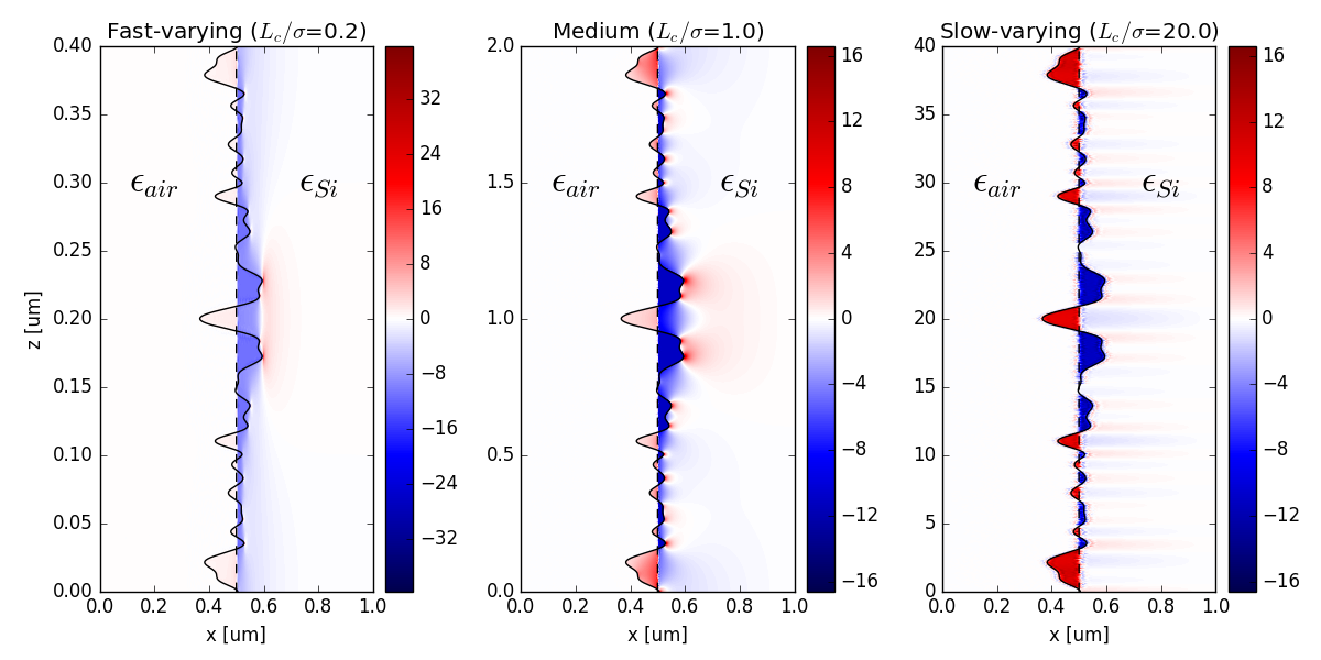
In the volume-current method, it is critically important to understand the nature of the perturbed dipole moments from perturbations at a dielectric interface. For small, localized perturbations (such as bumps or point-defects), the electric polarizability and relates the magnitude of the current source to the incident field. However, for roughness that exists along the entire interface, our goal is to understand the statistical properties of the ensemble of dipole moments in the quasi-static limit. In the following, we computationally verify that the flat shifted-interface polarizability is an accurate approximation for Gaussian-correlated randomly rough sidewalls so long as the correlation length is considerably larger than the root-mean-square (RMS) amplitude of the perturbation height .
To determine the appropriate limits for which the flat-shifted interface is valid, we determined the Fourier components of the 1-dimensional electrostatic polarizability density (along the interface-direction) by numerically computing the induced dipole moment density (per unit length) for randomly generated surfaces. Zero-mean sidewall functions with a Gaussian autocorrelation function were generated to represent the roughness profile, where is the root mean square (RMS) roughness amplitude and denotes the roughness correlation length [97]. This was done by filtering Gaussian white noise with the appropriate filter functions specified by the desired roughness autocorrelation function [98, 99, 100, 101]. We then solved the corresponding electrostatic Poisson equation using FEniCS, an open-source partial differential equation solver [102], to obtain the resulting charge distribution for silicon/air interfaces with a sidewall profile , as shown in Figure S1. For perpendicular incident fields with constant field , we use periodic boundary conditions at the edges of the interface and Neumann boundary conditions for simulation boundaries parallel to the interface. For parallel incident fields with constant field , we specify the corresponding electrostatic potential via appropriate Dirichlet boundary conditions along the simulation boundaries. Each simulation window used was long and wide, with an adaptive finite-element mesh. The dipole moment density corresponding to each specific roughness profile was then computed from the spatial charge distribution through [62]:
| (S35) | ||||
| (S36) |
where is the pixel size along the interface, is the change in electrostatic polarization density () and is normal to the interface (perpendicular to ). In principle, we can use the same expression for both perpendicular and parallel components, but we found the above expressions converged faster at a given finite resolution. The dipole moment density per unit perturbation height is then related to the polarizability through (and likewise ). Using this technique, we also performed a set of validation tests on flat-shifted boundaries and cylindrical/square perturbations to ensure that our method (and mesh resolution) accurately reproduces the correct electrostatic polarizabilities.
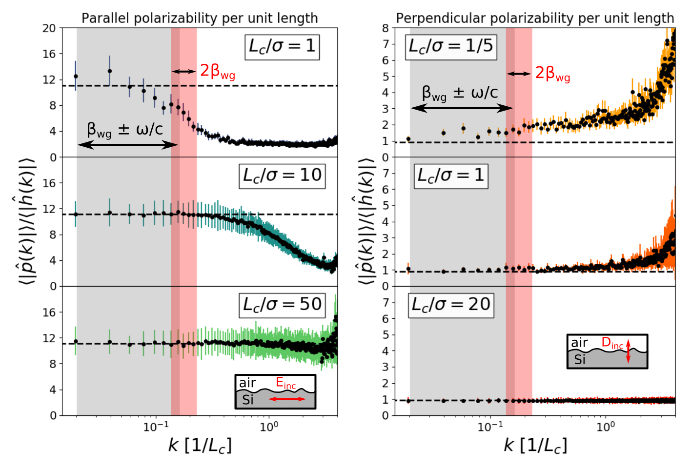
Using this technique to compute the induced dipole moment densities, we investigated the effect of different surface roughness statistics, quantified by the dimensionless ratio . Figure S2 shows the ratio of the averaged Fourier components (in spatial-frequency space) of the dipole moment density to the Fourier components of the surface profile . For a locally flat interface, the induced dipole moments are proportional to the perturbed height, and so far from we expect . In the limit of long correlation lengths (large ) our computations recover the expected polarizability of a flat-shifted interface, shown by dashed black lines in Figure S2. In general, the surface roughness will act as a diffraction grating [61] that couples incident light of wavevector to with a strength proportional to the roughness induced dipole moment . However, light can only be scattered into the light cone or reflected back into the waveguide, which limits the relevant frequency components to being within (far-field radiation) and at (reflection). The appropriate ranges for all waveguide geometries considered in the main text are depicted by the shaded regions in Figure S2 (assuming a roughness correlation length of =75 nm and =1550 nm).
As , it must be true that the locally flat result is recovered. In our analysis, we observe the useful result that for even relatively short correlation lengths on the order of , the Fourier components of the numerically computed polarizability match the simple shifted-boundary approximation by % for the interface-parallel components and % for the interface-perpendicular components. In state-of-the-art SOI waveguides, the correlation length of line-edge roughness was experimentally assessed to be between 50 to 100 nm, whereas the root mean square (RMS) roughness is typically between 0.5 to 2 nm [63, 64, 18, 65], corresponding to ratios on the order of 25–200. Therefore, we may accurately model the roughness-induced effective current-sources as flat-shifted interfaces for a large number of practical silicon photonic waveguide devices.
S4 Volume-current method calculations
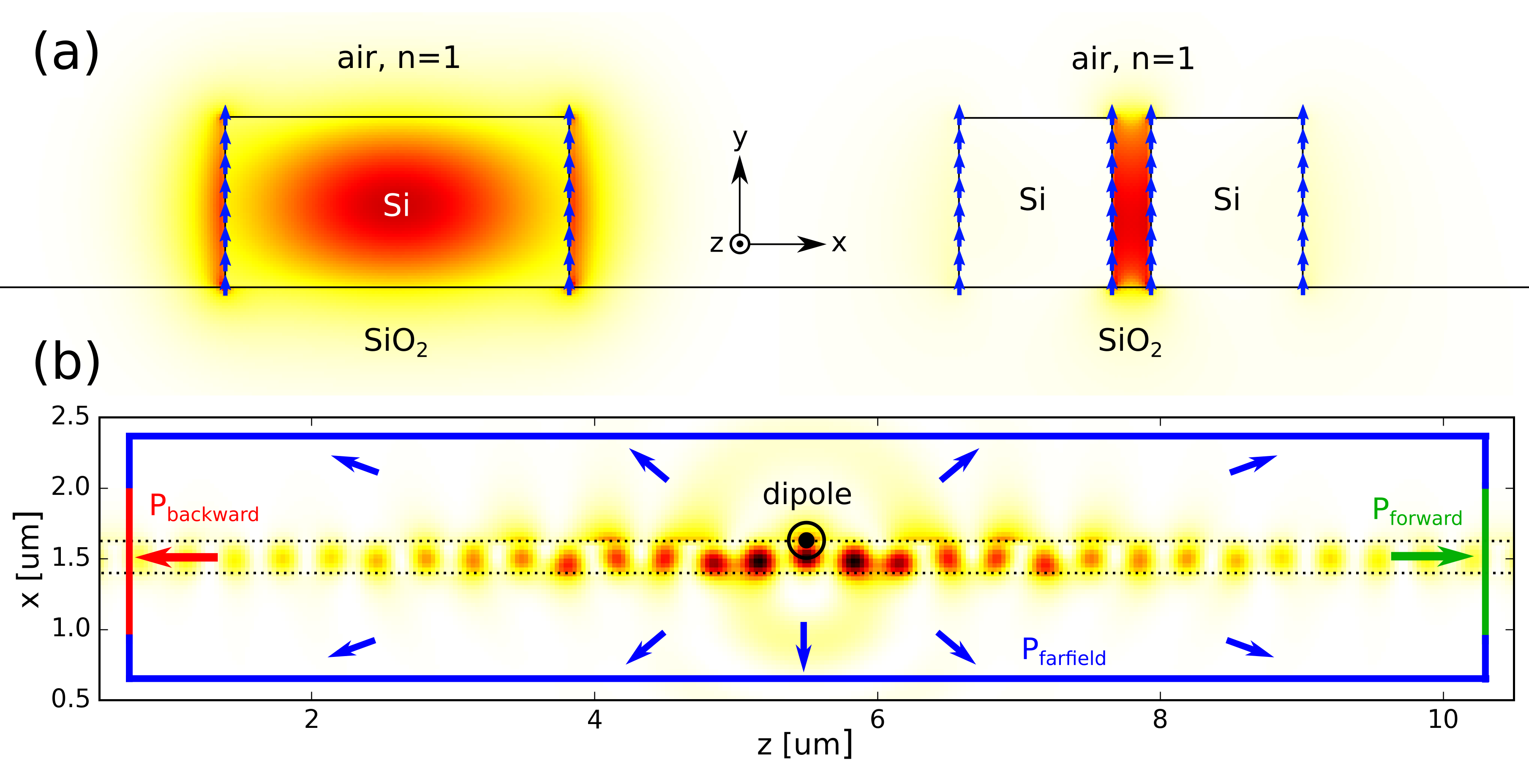
The relative scattering losses for each waveguide structure was determined by calculating the relative powers per unit volume of sidewall roughness (defined as the volume of the “bumps” on a surface) scattered into both the far-field and reflected backwards in the waveguide . We restricted our focus to vertically symmetric (-direction symmetric) line-edge roughness, and therefore modeled the roughness with 1-dimensional line current sources (in all 3-directions) with corresponding local amplitudes and phases proportional to the modal electric field, as depicted in Figure S3(a). The electric and displacement field of each waveguide mode was computed using the MIT Photonic Bands software package [103], and special care was taken to ensure that the normalization of the 3-dimensional SWG modes are equivalent to the normalization of the 2-dimensional strip and slot waveguide modes. We also make sure to normalize the input modal fields by power, rather than energy, to properly account for group velocity effects, and since our metric of interest is the scattered power per unit input power . The current-source is determined by:
| (S37) |
For each waveguide geometry and each inequivalent sidewall position, the corresponding line of current sources is then simulated using MEEP, a freely available finite-difference time domain (FDTD) software package [104]. The amount of power scattered into the far-field, versus forward and backward scattered power are determined by monitoring the power flux (at a wavelength of 1550 nm) through the simulation boundaries, as shown in Figure S3(b). Each FDTD simulation is computed with a resolution of 32 pixels/m and a domain size of 10 m 2.5 m 2.5 m with perfectly matched layers (PML) at the boundaries, except for SWGs where we place adiabatic absorbers at the and boundaries. The total power loss (the sum of the far-field power and the reflected power ) is then averaged over all sidewall positions and computed per unit waveguide length.
Acknowledgments
We would like to thank Alexander McCauley for originating the polarization-statistics approach for roughness with short correlation lengths.
This work is supported by the National Science Foundation under Award No. 1709212 and in part by the Army Research Office under contract number W911NF-13-D-0001.
References
- [1] C. A. Barrios, K. B. Gylfason, B. Sánchez, A. Griol, H. Sohlström, M. Holgado, and R. Casquel, “Slot-waveguide biochemical sensor,” Optics Letters, vol. 32, no. 21, p. 3080, 2007.
- [2] T. Claes, J. G. Molera, K. De Vos, E. Schacht, R. Baets, and P. Bienstman, “Label-free biosensing with a slot-waveguide-based ring resonator in silicon on insulator,” IEEE Photonics Journal, vol. 1, no. 3, pp. 197–204, 2009.
- [3] C. F. Carlborg, K. B. Gylfason, A. Kaźmierczak, F. Dortu, M. J. Bañuls Polo, A. Maquieira Catala, G. M. Kresbach, H. Sohlström, T. Moh, L. Vivien, J. Popplewell, G. Ronan, C. A. Barrios, G. Stemme, and W. van der Wijngaart, “A packaged optical slot-waveguide ring resonator sensor array for multiplex label-free assays in labs-on-chips,” Lab Chip, vol. 10, no. 3, pp. 281–290, 2010.
- [4] F. Dell’Olio and V. M. Passaro, “Optical sensing by optimized silicon slot waveguides,” Optics Express, vol. 15, no. 8, p. 4977, 2007.
- [5] Q. Liu, X. Tu, K. W. Kim, J. S. Kee, Y. Shin, K. Han, Y. J. Yoon, G. Q. Lo, and M. K. Park, “Highly sensitive Mach–Zehnder interferometer biosensor based on silicon nitride slot waveguide,” Sensors and Actuators, B: Chemical, vol. 188, pp. 681–688, 2013.
- [6] C. A. Barrios, M. J. Bañuls, V. González-Pedro, K. B. Gylfason, B. Sánchez, A. Griol, A. Maquieira, H. Sohlström, M. Holgado, and R. Casquel, “Label-free optical biosensing with slot-waveguides,” Optics Letters, vol. 33, no. 7, p. 708, 2008.
- [7] J. G. Wangüemert-pérez, P. Cheben, A. Ortega-moñux, C. Alonso-ramos, D. Pérez-galacho, R. Halir, I. Molina-fernández, D.-x. Xu, and J. H. Schmid, “Evanescent field waveguide sensing with subwavelength grating structures in silicon-on-insulator,” Optics Letters, vol. 39, no. 15, pp. 4442–4445, 2014.
- [8] J. Flueckiger, S. Schmidt, V. Donzella, A. Sherwali, D. M. Ratner, L. Chrostowski, and K. C. Cheung, “Sub-wavelength grating for enhanced ring resonator biosensor,” Optics Express, vol. 24, no. 14, p. 15672, 2016.
- [9] H. Yan, L. Huang, X. Xu, S. Chakravarty, N. Tang, H. Tian, and R. T. Chen, “Unique surface sensing property and enhanced sensitivity in microring resonator biosensors based on subwavelength grating waveguides,” Optics Express, vol. 24, no. 26, p. 29724, 2016.
- [10] A. Dhakal, A. Raza, F. Peyskens, A. Z. Subramanian, S. Clemmen, N. Le Thomas, and R. Baets, “Efficiency of evanescent excitation and collection of spontaneous Raman scattering near high index contrast channel waveguides,” Optics Express, vol. 23, no. 21, p. 27391, 2015.
- [11] D. Marcuse, “Mode conversion caused by surface imperfections of a dielectric slab waveguide,” The Bell System Technical Journal, no. December, pp. 3187–3215, 1969.
- [12] A. W. Snyder and J. D. Love, Optical waveguide theory. London: Chapman and Hall, 1983.
- [13] F. Payne and J. P. R. Lacey, “A theoretical analysis of scattering loss from planar optical waveguides,” Optical and Quantum Electronics, vol. 26, pp. 977–986, 1994.
- [14] S. G. Johnson, M. L. Povinelli, M. Soljacic, A. Karalis, S. Jacobs, and J. D. Joannopoulos, “Roughness losses and volume-current methods in photonic-crystal waveguides,” Applied Physics B: Lasers and Optics, vol. 81, no. 2-3, pp. 283–293, 2005.
- [15] K. K. Lee, D. R. Lim, H.-C. Luan, A. Agarwal, J. Foresi, and L. C. Kimerling, “Effect of size and roughness on light transmission in a Si/SiO2 waveguide: Experiments and model,” Applied Physics Letters, vol. 77, no. 11, pp. 1617–1619, 2000.
- [16] K. K. Lee, D. R. Lim, and L. C. Kimerling, “Fabrication of ultralow-loss Si/SiO2 waveguides by roughness reduction,” Optics Letters, vol. 26, no. 23, pp. 1888–1890, 2001.
- [17] F. Morichetti, A. Canciamilla, C. Ferrari, M. Torregiani, A. Melloni, and M. Martinelli, “Roughness induced backscattering in optical silicon waveguides,” Physical Review Letters, vol. 104, no. 3, pp. 1–4, 2010.
- [18] D. H. Lee, S. J. Choo, U. Jung, K. W. Lee, K. W. Kim, and J. H. Park, “Low-loss silicon waveguides with sidewall roughness reduction using a SiO2 hard mask and fluorine-based dry etching,” Journal of Micromechanics and Microengineering, vol. 25, no. 1, 2015.
- [19] P. Berini, “Figures of merit for surface plasmon waveguides,” Optics Express, vol. 14, no. 26, pp. 13030–13042, 2006.
- [20] W. L. Barnes, “Surface plasmon–polariton length scales: A route to sub-wavelength optics,” Journal of Optics A: Pure and Applied Optics, vol. 8, pp. S87–S93, 2006.
- [21] P. Offermans, M. C. Schaafsma, S. R. K. Rodriguez, Y. Zhang, M. Crego-Calama, S. H. Brongersma, and J. G. Rivas, “Universal scaling of the figure of merit of plasmonic sensors,” ACS Nano2, vol. 5, no. 6, pp. 5151–5157, 2011.
- [22] R. Zafar and M. Salim, “Enhanced figure of merit in Fano resonance-based plasmonic refractive index sensor,” IEEE Sensors Journal, vol. 15, no. 11, pp. 6313–6317, 2015.
- [23] M. Islam, D. R. Chowdhury, A. Ahmad, and G. Kumar, “Terahertz plasmonic waveguide based thin film sensor,” Journal of Lightwave Technology, vol. 35, no. 23, pp. 5215–5221, 2017.
- [24] Z. Zhang, J. Yang, X. He, J. Zhang, J. Huang, D. Chen, and Y. Han, “Plasmonic refractive index sensor with high figure of merit based on concentric-rings resonator,” Sensors, vol. 18, no. 116, pp. 1–14, 2018.
- [25] J. Hu, X. Sun, A. Agarwal, and L. C. Kimerling, “Design guidelines for optical resonator biochemical sensors,” Journal of the Optical Society of America, vol. 26, no. 5, pp. 1032–1041, 2009.
- [26] A. Nitkowski, A. Baeumner, and M. Lipson, “On-chip spectrophotometry for bioanalysis using microring resonators,” Biomedical Optics Express, vol. 2, pp. 271–277, jan 2011.
- [27] L. Huang, H. Tian, D. Yang, J. Zhou, Q. Liu, P. Zhang, and Y. Ji, “Optimization of figure of merit in label-free biochemical sensors by designing a ring defect coupled resonator,” Optics Communications, vol. 332, pp. 42–49, 2014.
- [28] A. Z. Subramanian, E. Ryckeboer, A. Dhakal, F. Peyskens, A. Malik, B. Kuyken, H. Zhao, S. Pathak, A. Ruocco, A. De Groote, P. Wuytens, D. Martens, F. Leo, W. Xie, U. D. Dave, M. Muneeb, P. Van Dorpe, J. Van Campenhout, W. Bogaerts, P. Bienstman, N. Le Thomas, D. Van Thourhout, Z. Hens, G. Roelkens, and R. Baets, “Silicon and silicon nitride photonic circuits for spectroscopic sensing on-a-chip,” Photonics Research, vol. 3, no. 5, p. B47, 2015.
- [29] C. Koos, P. Vorreau, T. Vallaitis, P. Dumon, W. Bogaerts, R. Baets, B. Esembeson, I. Biaggio, T. Michinobu, F. Diederich, W. Freude, and J. Leuthold, “All-optical high-speed signal processing with silicon–organic hybrid slot waveguides,” Nature Photonics, vol. 3, no. April, pp. 216–219, 2009.
- [30] R. Guo, B. Wang, X. Wang, L. Wang, L. Jiang, and Z. Zhou, “Optical amplification in Er/Yb silicate slot waveguide,” Optics Letters, vol. 37, no. 9, pp. 1427–1429, 2012.
- [31] S. Johnson, M. Ibanescu, M. Skorobogatiy, O. Weisberg, J. Joannopoulos, and Y. Fink, “Perturbation theory for Maxwell’s equations with shifting material boundaries,” Physical Review E, vol. 65, p. 066611, jun 2002.
- [32] P. Hanggi and P. Jung, “Colored noise in dynamical-systems,” in Advances in Chemical Physics, pp. 239–326, John Wiley & Sons, Inc., 1994.
- [33] A. Dhakal, A. Z. Subramanian, P. Wuytens, F. Peyskens, N. L. Thomas, and R. Baets, “Evanescent excitation and collection of spontaneous Raman spectra using silicon nitride nanophotonic waveguides,” Optics Letters, vol. 39, no. 13, pp. 4025–4028, 2014.
- [34] S. A. Holmstrom, T. H. Stievater, D. A. Kozak, M. W. Pruessner, N. Tyndall, W. S. Rabinovich, R. A. Mcgill, and J. B. Khurgin, “Trace gas Raman spectroscopy using functionalized waveguides,” Optica, vol. 3, no. 8, pp. 891–896, 2016.
- [35] C. C. Evans, C. Liu, and J. Suntivich, “TiO2 nanophotonic sensors for efficient integrated evanescent Raman spectroscopy,” ACS Photonics, vol. 3, no. 9, pp. 1662–1669, 2016.
- [36] N. M. Hanumegowda, C. J. Stica, B. C. Patel, I. White, and X. Fan, “Refractometric sensors based on microsphere resonators,” Applied Physics Letters, vol. 87, no. 20, p. 201107, 2005.
- [37] V. Passaro, B. Troia, M. La Notte, and F. De Leonardis, “Photonic resonant microcavities for chemical and biochemical sensing,” RSC Advances, vol. 3, pp. 25–44, 2012.
- [38] R. G. Heideman and P. V. Lambeck, “Remote opto-chemical sensing with extreme sensitivity: Design, fabrication and performance of a pigtailed integrated optical phase-modulated Mach–Zehnder interferometer system,” Sensors and Actuators, B: Chemical, vol. 61, pp. 100–127, 1990.
- [39] H. Lu, X. Liu, D. Mao, and G. Wang, “Plasmonic nanosensor based on Fano resonance in waveguide-coupled resonators,” Optics Letters, vol. 37, no. 18, pp. 3780–3782, 2012.
- [40] V. Singh, P. T. Lin, N. Patel, H. Lin, L. Li, Y. Zou, F. Deng, C. Ni, J. Hu, J. Giammarco, A. P. Soliani, B. Zdyrko, I. Luzinov, S. Novak, J. Novak, P. Wachtel, S. Danto, J. D. Musgraves, K. Richardson, L. C. Kimerling, and A. M. Agarwal, “Mid-infrared materials and devices on a Si platform for optical sensing,” Science and Technology of Advanced Materials, vol. 15, no. 1, p. 014603, 2014.
- [41] P. Kozma, F. Kehl, E. Ehrentreich-Förster, C. Stamm, and F. F. Bier, “Biosensors and bioelectronics integrated planar optical waveguide interferometer biosensors : A comparative review,” Biosensors and Bioelectronics, vol. 58, pp. 287–307, 2014.
- [42] F. T. Dullo, S. Lindecrantz, J. Jana, J. H. Hansen, M. Engqvist, S. A. Solbø, and G. Hellesø, “Sensitive on-chip methane detection with a cryptophane-A cladded Mach–Zehnder interferometer,” Optics Express, vol. 23, no. 24, pp. 31564–31573, 2015.
- [43] A. R. Bastos, C. M. S. Vicente, R. Oliveira-Silva, N. J. O. Silva, M. Tacao, J. P. da Costa, M. Lima, P. S. Andre, and R. A. S. Ferreira, “Integrated optical Mach–Zehnder interferometer based on organic-inorganic hybrids for photonics-on-a-chip biosensing applications,” Sensors, vol. 18, no. 840, pp. 1–11, 2018.
- [44] R. J. Bojko, J. Li, L. He, T. Baehr-jones, M. Hochberg, and Y. Aida, “Electron beam lithography writing strategies for low loss, high confinement silicon optical waveguides,” Journal of Vacuum Science & Technology B: Microelectronics and Nanometer Structures, vol. 29, no. 6, pp. 1–6, 2011.
- [45] E. Ryckeboer, R. Bockstaele, M. Vanslembrouck, and R. Baets, “Glucose sensing by waveguide-based absorption spectroscopy on a silicon chip.,” Biomedical Optics Express, vol. 5, pp. 1636–48, may 2014.
- [46] W. Weber, S. McCarthy, and G. Ford, “Perturbation theory applied to gain or loss in an optical waveguide,” Applied Optics, vol. 13, no. 4, pp. 715–716, 1974.
- [47] A. Kumar, S. I. Hosain, and A. K. Ghatak, “Propagation characteristics of weakly guiding lossy fibres: An exact and perturbation analysis,” Optica Acta, vol. 28, no. 4, pp. 559–566, 1981.
- [48] Z. Pantic and R. Mittra, “Quasi-TEM analysis of microwave transmission lines by the finite-element method,” IEEE Transactions on Microwave Theory and Techniques1, vol. MTT-34, no. 11, pp. 1096–1103, 1986.
- [49] S. X. She, “Propagation loss in metal-clad waveguides and weakly absorptive waveguides by a perturbation method,” Optics Letters, vol. 15, no. 16, pp. 900–902, 1990.
- [50] V. L. Gupta and E. K. Sharma, “Metal-clad and absorptive multilayer waveguides: an accurate perturbation analysis,” Journal of the Optical Society of America, vol. 9, no. 6, pp. 953–956, 1992.
- [51] C. Themistos, B. M. A. Rahman, A. Hadjicharalambous, K. Thomas, and V. Grattan, “Loss/gain characterization of optical waveguides,” Journal of Lightwave Technology, vol. 13, no. 8, pp. 1760–1765, 1995.
- [52] S. Johnson, M. Ibanescu, M. Skorobogatiy, O. Weisberg, T. Engeness, M. Soljačić, S. Jacobs, J. Joannopoulos, and Y. Fink, “Low-loss asymptotically single-mode propagation in large-core OmniGuide fibers,” Optics Express, vol. 9, no. 13, pp. 748–779, 2001.
- [53] J. T. Robinson, K. Preston, O. Painter, and M. Lipson, “First-principle derivation of gain in high-index- contrast waveguides,” Optics Express, vol. 16, no. 21, pp. 16659–16669, 2008.
- [54] D. Melati, A. Melloni, and F. Morichetti, “Real photonic waveguides: Guiding light through imperfections,” Advances in Optics and Photonics, vol. 6, p. 131, 2014.
- [55] M. Borselli, T. J. Johnson, and O. Painter, “Beyond the Rayleigh scattering limit in high-Q silicon microdisks: theory and experiment,” Optics Express, vol. 13, no. 5, pp. 1515–1530, 2005.
- [56] H. Lee, T. Chen, J. Li, O. Painter, and K. J. Vahala, “Ultra-low-loss optical delay line on a silicon chip,” Nature Communications, vol. 3, no. May, p. 867, 2012.
- [57] J. F. Bauters, M. J. R. Heck, D. John, D. Dai, M.-c. Tien, J. S. Barton, A. Leinse, R. G. Heideman, D. J. Blumenthal, and J. E. Bowers, “Ultra-low-loss high-aspect-ratio Si3N4 waveguides,” Optics Express, vol. 19, no. 4, pp. 3163–3174, 2011.
- [58] K. Wörhoff, R. G. Heideman, A. Leinse, and M. Hoekman, “TriPleX: a versatile dielectric photonic platform,” Advanced Optical Technologies, vol. 4, no. 2, pp. 189–207, 2015.
- [59] J. Hu, V. Tarasov, N. Carlie, N.-N. Feng, L. Petit, A. Agarwal, K. Richardson, and L. Kimerling, “Si-CMOS-compatible lift-off fabrication of low-loss planar chalcogenide waveguides,” Optics Express, vol. 15, no. 19, pp. 11798–11807, 2007.
- [60] C. C. Evans, C. Liu, and J. Suntivich, “Low-loss titanium dioxide waveguides and resonators using a dielectric lift-off fabrication process,” Optics Express, vol. 23, no. 9, pp. 11160–11169, 2015.
- [61] J. P. R. Lacey and F. P. Payne, “Radiation loss from planar waveguides with random wall imperfections,” IEEE Proceedings, vol. 137, no. 4, pp. 282–288, 1990.
- [62] J. D. Jackson, Classical electrodynamics. John Wiley & Sons, Inc., 3rd ed., 1999.
- [63] F. Xia, L. Sekaric, and Y. Vlasov, “Ultracompact optical buffers on a silicon chip,” Nature Photonics, vol. 1, no. 1, pp. 65–71, 2007.
- [64] M. G. Wood, L. Chen, J. R. Burr, and R. M. Reano, “Optimization of electron beam patterned hydrogen silsesquioxane mask edge roughness for low-loss silicon waveguides,” Journal of Nanophotonics, vol. 8, no. 1, p. 083098, 2014.
- [65] P. Wang, A. Michael, and C. Y. Kwok, “Fabrication of sub-micro silicon waveguide with vertical sidewall and reduced roughness for low loss applications,” Procedia Engineering, vol. 87, no. 612, pp. 979–982, 2014.
- [66] T. Barwicz and H. I. Smith, “Evolution of line-edge roughness during fabrication of high-index-contrast microphotonic devices,” Journal of Vacuum Science & Technology B: Microelectronics and Nanometer Structures, vol. 21, no. 6, pp. 2892 – 2896, 2003.
- [67] G. P. Patsis, V. Constantoudis, A. Tserepi, E. Gogolides, and G. Grozev, “Quantification of line-edge roughness of photoresists. I. A comparison between off-line and on-line analysis of top-down scanning electron microscopy images,” Journal of Vacuum Science & Technology B: Microelectronics and Nanometer Structures, vol. 21, no. 3, pp. 1008 – 1018, 2003.
- [68] V. Constantoudis, G. P. Patsis, A. Tserepi, and E. Gogolides, “Quantification of line-edge roughness of photoresists. II. Scaling and fractal analysis and the best roughness descriptors,” Journal of Vacuum Science & Technology B: Microelectronics and Nanometer Structures, vol. 21, no. 3, pp. 1019 – 1026, 2003.
- [69] P. Dumon, W. Bogaerts, V. Wiaux, J. Wouters, S. Beckx, J. V. Campenhout, D. Taillaert, B. Luyssaert, P. Bienstman, and D. V. Thourhout, “Low-loss SOI photonic wires and ring resonators fabricated with deep UV lithography,” IEEE Photonics Technology Letters, vol. 16, no. 5, pp. 1328–1330, 2004.
- [70] A. Oskooi and S. G. Johnson, Chapter 4: Electromagnetic Wave Source Conditions. Artech House, 2013.
- [71] S. Sardo, F. Giacometti, S. Doneda, U. Colombo, M. Di, A. Donghi, R. Morson, G. Mutinati, A. Nottola, M. Gentili, and M. C. Ubaldi, “Line edge roughness (LER) reduction strategy for SOI waveguides fabrication,” Microelectronic Engineering, vol. 85, pp. 1210–1213, 2008.
- [72] T. Alasaarela, D. Korn, L. Alloatti, A. Tervonen, R. Palmer, J. Leuthold, W. Freude, and S. Honkanen, “Reduced propagation loss in silicon strip and slot waveguides coated by atomic layer deposition,” Optics Express, vol. 19, no. 12, pp. 11529–11538, 2011.
- [73] K. Debnath, A. Z. Khokhar, S. A. Boden, H. Arimoto, S. Z. Oo, H. M. H. Chong, G. T. Reed, and S. Saito, “Low-loss slot waveguides with silicon (111) surfaces realized using anisotropic wet etching,” Frontiers in Materials, vol. 3, no. November, pp. 1–5, 2016.
- [74] T. Baehr-jones, M. Hochberg, C. Walker, and A. Scherer, “High-Q optical resonators in silicon-on-insulator-based slot waveguides,” Applied Physics Letters, vol. 86, no. 081101, pp. 1–3, 2005.
- [75] R. Ding, T. Baehr-jones, W.-J. Kim, X. Xiong, R. Bojko, J.-M. Fedeli, M. Fournier, and M. Hochberg, “Low-loss strip-loaded slot waveguides in silicon-on-insulator,” Optics Express, vol. 18, no. 24, pp. 25061–25067, 2010.
- [76] P. J. Bock, P. Cheben, J. H. Schmid, J. Lapointe, A. Delâge, S. Janz, G. C. Aers, D.-X. Xu, A. Densmore, and T. J. Hall, “Subwavelength grating periodic structures in silicon-on-insulator: a new type of microphotonic waveguide,” Optics Express, vol. 18, no. 19, pp. 20251–20262, 2010.
- [77] M. Gnan, S. Thoms, D. S. Macintyre, R. M. De La Rue, and M. Sorel, “Fabrication of low-loss photonic wires in silicon-on-insulator using hydrogen silsesquioxane electron-beam resist,” Electronics Letters, vol. 44, no. 2, pp. 115–116, 2008.
- [78] A. Yariv, “Universal relations for coupling of optical power between microresonators and dielectric waveguides,” Electronics Letters, vol. 36, no. 4, pp. 321–322, 2000.
- [79] Q. Li, A. A. Eftekhar, Z. Xia, and A. Adibi, “Azimuthal-order variations of surface-roughness-induced mode splitting and scattering loss in high-Q microdisk resonators,” Optics letters, vol. 37, no. 9, pp. 1586–1588, 2012.
- [80] E. Jaberansary, T. M. B. Masaud, M. M. Milosevic, M. Nedeljkovic, G. Z. Mashanovich, and H. M. H. Chong, “Scattering loss estimation using 2-D Fourier analysis and modeling of sidewall roughness on optical waveguides,” IEEE Photonics Journal, vol. 5, no. 3, 2013.
- [81] H. Zhao, S. Clemmen, A. Raza, and R. Baets, “Stimulated Raman spectroscopy of analytes evanescently probed by a silicon nitride photonic integrated waveguide,” Optics Letters, vol. 43, no. 6, pp. 1403–1406, 2018.
- [82] A. Dhakal, F. Peyskens, A. Z. Subramanian, N. L. Thomas, and R. Baets, “Enhancement of light absorption, scattering and emission in high index contrast waveguides,” in OSA Advanced Photonics Congress, pp. 1–3, 2013.
- [83] Q. Du, Y. Huang, O. Ogbuu, W. Zhang, J. Li, V. Singh, A. M. Agarwal, and J. Hu, “Gamma radiation effects in amorphous silicon and silicon nitride photonic devices,” Optics Letters, vol. 42, no. 3, pp. 587–590, 2017.
- [84] J. Hu, N. Carlie, L. Petit, A. Agarwal, K. Richardson, and L. C. Kimerling, “Cavity-enhanced infrared absorption in planar chalcogenide glass microdisk resonators: Experiment and analysis,” Journal of Lightwave Technology, vol. 27, no. 23, pp. 5240–5245, 2009.
- [85] B. Eggleton, B. Luther-Davies, and K. Richardson, “Chalcogenide photonics,” Nature Photonics, vol. 5, pp. 141–148, dec 2011.
- [86] Y.-C. Chang, V. Paeder, L. Hvozdara, J.-M. Hartmann, and H. P. Herzig, “Low-loss germanium strip waveguides on silicon for the mid-infrared,” Optics Letters, vol. 37, no. 14, pp. 2883–2885, 2012.
- [87] Q. Liu, J. M. Ramirez, V. Vakarin, X. L. Roux, A. Ballabio, J. Frigerio, D. Chrastina, G. Isella, D. Bouville, L. Vivien, C. A. Ramos, and D. Marris-Morini, “Mid-infrared sensing between 5.2 and 6.6 m wavelengths using Ge-rich SiGe waveguides,” Optical Materials Express, vol. 8, no. 5, pp. 1305–1312, 2018.
- [88] T. Baehr-Jones, A. Spott, R. Ilic, A. Spott, B. Penkov, W. Asher, and M. Hochberg, “Silicon-on-sapphire integrated waveguides for the mid-infrared.,” Optics Express, vol. 18, no. 12, pp. 12127–12135, 2010.
- [89] F. Meng, R.-J. Shiue, N. Wan, L. Li, J. Nie, N. C. Harris, E. H. Chen, T. Schröder, N. Pervez, I. Kymissis, D. Englund, N. Pervez, I. Kymissis, and D. Englund, “Waveguide-integrated photonic crystal spectrometer with camera readout,” Applied Physics Letters, vol. 105, no. 051103, 2014.
- [90] R. Sun, P. Dong, N.-N. Feng, C.-Y. Hong, M. Lipson, and L. Kimerling, “Horizontal single and multiple slot waveguides: Optical transmission at = 1550 nm,” Optics Express, vol. 15, no. 26, pp. 17967–17972, 2007.
- [91] H. Lin, Z. Luo, T. Gu, L. C. Kimerling, K. Wada, A. Agarwal, and J. Hu, “Mid-infrared integrated photonics on silicon: A perspective,” Nanophotonics, vol. 7, no. 2, 2017.
- [92] M. Saleh, B.E.A. and Teich, Fundamentals of Photonics. John Wiley & Sons, Inc., 2nd ed., 2007.
- [93] Y. C. Jun, R. M. Briggs, H. A. Atwater, and M. L. Brongersma, “Broadband enhancement of light emission in silicon slot waveguides,” Optics Express, vol. 17, no. 9, pp. 7479–7490, 2009.
- [94] R. C. McPhedran, L. C. Botten, J. Mcorist, A. A. Asatryan, C. M. D. Sterke, and N. A. Nicorovici, “Density of states functions for photonic crystals,” Physical Review E, vol. 69, no. 016609, pp. 1–16, 2004.
- [95] G. B. Arfken and H.-J. Weber, Mathematical methods for physicists. Academic Press, 5th ed., 2000.
- [96] J. R. Ferraro, Introductory raman spectroscopy. Academic Press, 2nd ed., 2002.
- [97] A. V. Oppenheim, R. W. Schafer, and J. R. Buck, Discrete-time signal processing. Upper Saddle River, New Jersey: Prentice-Hall, Inc., 2nd ed., 1999.
- [98] K. Y. R. Billah and M. Shinozuka, “Numerical method for colored-noise generation and its application to a bistable system,” Rapid Communications, vol. 42, no. 12, pp. 7492–7495, 1990.
- [99] N. J. Kasin, “Discrete simulation of colored noise and stochastic processes and power law noise generation,” Proceedings of the IEEE, vol. 83, no. 5, pp. 802–827, 1995.
- [100] D. J. Young and N. C. Beaulieu, “The generation of correlated rayleigh random variates by inverse discrete Fourier transform,” IEEE Transactions on Communications, vol. 48, no. 7, pp. 1114–1127, 2000.
- [101] K. Lu and J.-D. Bao, “Numerical simulation of generalized Langevin equation with arbitrary correlated noise,” Physical Review E, vol. 72, no. 067701, pp. 1–4, 2005.
- [102] M. S. Alnaes, J. Blechta, J. Hake, A. Johansson, B. Kehlet, A. Logg, C. Richardson, J. Ring, M. E. Rognes, and G. N. Wells, “The FEniCS project version 1.5,” Archive of Numerical Software, vol. 3, no. 100, pp. 9–23, 2015.
- [103] S. Johnson and J. Joannopoulos, “Block-iterative frequency-domain methods for Maxwell’s equations in a planewave basis,” Optics Express, vol. 8, no. 3, p. 173, 2001.
- [104] A. F. Oskooi, D. Roundy, M. Ibanescu, P. Bermel, J. D. Joannopoulos, and S. G. Johnson, “Meep: A flexible free-software package for electromagnetic simulations by the FDTD method,” Computer Physics Communications, vol. 181, no. 3, pp. 687–702, 2010.