Experimental Characterization, Optimization, and Recovery
of Data Retention Errors in MLC NAND Flash Memory
Abstract
This paper summarizes our work on experimentally characterizing, mitigating, and recovering data retention errors in multi-level cell (MLC) NAND flash memory, which was published in HPCA 2015 [10], and examines the work’s significance and future potential. Retention errors, caused by charge leakage over time, are the dominant source of flash memory errors. Understanding, characterizing, and reducing retention errors can significantly improve NAND flash memory reliability and endurance. In this work, we first characterize, with real 2Y-nm MLC NAND flash chips, how the threshold voltage distribution of flash memory changes with different retention ages – the length of time since a flash cell was programmed. We observe from our characterization results that 1) the optimal read reference voltage of a flash cell, using which the data can be read with the lowest raw bit error rate (RBER), systematically changes with its retention age, and 2) different regions of flash memory can have different retention ages, and hence different optimal read reference voltages.
Based on our findings, we propose two new techniques. First, Retention Optimized Reading (ROR) adaptively learns and applies the optimal read reference voltage for each flash memory block online. The key idea of ROR is to periodically learn a tight upper bound of the optimal read reference voltage, and from there approach the optimal read reference voltage. Our evaluations show that ROR can extend flash memory lifetime by 64% and reduce average error correction latency by 10.1%, with only 768 KB storage overhead in flash memory for a 512 GB flash-based SSD. Second, Retention Failure Recovery (RFR) recovers data with uncorrectable errors offline by identifying and probabilistically correcting flash cells with retention errors. Our evaluation shows that RFR reduces RBER by 50%, which essentially doubles the error correction capability, and thus can effectively recover data from otherwise uncorrectable flash errors.
1 Introduction
Over the past decade, the capacity of NAND flash memory has been increasing continuously, as a result of aggressive process scaling and the advent of multi-level cell (MLC) technology. This trend has enabled NAND flash memory to replace spinning disks for a wide range of applications – from high performance clusters and large-scale data centers to consumer PCs, laptops, and mobile devices. Unfortunately, as flash density increases, flash memory cells become more vulnerable to various types of device and circuit level noise [86, 8, 3, 4, 5] – e.g., retention noise [8, 12, 13, 80, 91, 3, 4, 5, 70], read disturb noise [91, 15, 6, 3, 4, 5], cell-to-cell program interference noise [8, 11, 14, 6, 3, 4, 5], and program/erase (P/E) cycling noise [8, 9, 3, 4, 5]. These are sources of errors that can significantly degrade NAND flash memory reliability.
A traditional solution to overcome flash errors, regardless of their source, is to use error-correcting codes (ECC) [30, 66, 3, 4, 5]. By storing a certain amount of redundant bits per unit data, ECC can detect and correct a limited number of raw bit errors. With the help of ECC, flash memory can hide these errors from the users until the number of errors per unit data exceeds the correction capability of the ECC. Flash memory designers have been relying on stronger ECC to compensate for lifetime reductions due to technology scaling. However, stronger ECC, which has higher capacity and implementation overhead, has diminishing returns on the amount of flash lifetime improvement [12, 13]. As such, we intend to look for more efficient ways of reducing flash errors.
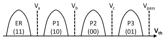
Retention errors, caused by charge leakage over time after a flash cell is programmed, are the dominant source of flash memory errors [8, 12, 13, 109, 3, 4, 5]. The amount of charge stored in a flash memory cell determines the threshold voltage level of the cell, which in turn represents the logical data value stored in the cell. As illustrated in Figure 1, the threshold voltage () range of a 2-bit MLC NAND flash cell is divided into four regions by three read reference voltages, , , and . The region in which the threshold voltage of a flash cell falls represents the cell’s current state, which can be ER (or erased), P1, P2, or P3. Each state decodes into a 2-bit value that is stored in the flash cell (e.g., 11, 10, 00, or 01).111A detailed background on NAND flash memory design and operation, and on data retention errors in NAND flash memory, can be found in our prior works [12, 11, 3, 4, 5].
As the manufacturing process technology for NAND flash memory scales to smaller feature sizes, the capacitance of a flash cell, and the number of electrons stored in the cell, decrease. State-of-the-art MLC flash memory cells can store only 100 electrons [10, 81]. Gaining or losing several electrons in a flash cell can significantly change the cell’s voltage level and eventually alter the state of the cell. In addition, MLC technology reduces the size of the threshold voltage window [9], i.e., the span of threshold voltage values corresponding to each logical state, in order to store more states in a single cell. This also makes the state of a cell more likely to shift due to charge loss caused by retention noise. As such, for NAND flash memory, retention errors are one of the most important limiting factors of more aggressive process scaling and MLC technology.
One way to reduce retention errors is to periodically read, correct, and reprogram the flash memory before the number of errors accumulated over time exceed the error correction capability of the ECC, i.e., the maximum number of raw bit errors tolerable by the ECC [12, 13, 69, 90]. However, this flash correct and refresh (FCR) technique has two major limitations: 1) FCR uses a fixed read reference voltage to read data under different retention ages, which is suboptimal, and 2) FCR requires the flash controller to be consistently powered on so that errors can be corrected, limiting its applicability to enterprise deployments that have always-on power supplies.
In our HPCA 2015 paper [10], we pursue a better understanding of retention error behavior to improve NAND flash reliability and lifetime, and find better (and complementary) ways to mitigate flash retention errors. We characterize 1) the distortion of threshold voltage distribution at different retention ages, i.e., the idle time after the data is programmed to the flash memory, for state-of-the-art 2Y-nm (20- to 24-nm) NAND flash memory chips at room temperature, and 2) the retention age distribution of flash pages using disk traces taken from real workloads. Our key findings are:
-
1.
Due to threshold voltage distribution distortion, the optimal read reference voltages of flash cells, at which the minimum raw bit error rate (RBER) can be achieved, systematically shift to lower values as retention age increases.
-
2.
Pages within the same flash block (the granularity at which flash memory can be erased) tend to have similar retention ages and hence similar optimal read reference voltages, whereas pages across different flash blocks have different optimal read reference voltages.
Based on our findings, we propose two mechanisms to mitigate data retention errors. First, we propose an online technique called Retention Optimized Reading (ROR). They key idea of ROR is to reduce the raw bit error rate by adaptively learning and applying the optimal read reference voltage for each flash block. Our evaluations show that ROR extends flash lifetime by 64% and reduces average error correction latency by 10.1%, with only 768 KB storage overhead for a 512 GB flash-based SSD. Second, we propose an offline error recovery technique called Retention Failure Recovery (RFR). The key idea of RFR is to identify fast- and slow-leaking cells and probabilistically determine the original value of an erroneous cell based on its leakage-speed property and its threshold voltage. Our evaluations show that RFR can effectively reduce the average raw bit error rate (RBER) by 50%, essentially doubling the error correction capability of flash memory, and allowing for the recovery of data otherwise uncorrectable by ECC.
2 Flash Data Retention Characterization
We use an FPGA-based flash memory testing platform to characterize real state- of-the-art 2Y-nm NAND flash memory chips [7, 8]. As absolute threshold voltage values are proprietary information to NAND flash vendors, we present our results using normalized voltages, where the nominal maximum value of is equal to 512 in our normalized scale, and where 0 represents GND. Section 3.1 of our HPCA 2015 paper [10] provides a detailed description of our experimental methodology.
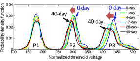
Figure 2 shows the threshold voltage distribution of flash memory at different retention ages for 8,000 P/E cycles. We make two observations from the figure. First, for the higher-voltage states (P2 and P3), their threshold voltage distributions systematically shift to lower voltage values as the retention age grows. Second, the distributions of each state become wider with higher retention age, and that the distributions of states at higher voltage (e.g., P3) shift faster than those of states at lower voltage (e.g., P1).
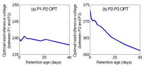
We find that these changes due to retention leakage have an impact to the optimal read reference voltage (OPT), which is the read reference voltage between two states that minimizes the raw bit error rate (RBER). Figure 3 shows the optimal read reference voltage over retention age. We make two observations from the figure. First, Figure 3a shows a slightly decreasing trend of P1–P2 OPT (the optimal read reference voltage used to distinguish between cells in the P1 state and cells in the P2 state) over retention age. Second, we observe that P2–P3 OPT decreases much more rapidly with retention age than P1–P2 OPT, as shown in Figure 3b.
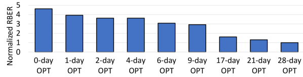
As the distributions continue to shift with growing retention age, the OPT for one retention age will be different than the OPT for a different age, suggesting that a dynamically changing OPT is ideal. To quantify how the choice of read reference voltage affects RBER, we apply the optimal read reference voltages (OPTs) determined for {0, 1, 2, 6, 9, 17, 21, 28}-day retention ages to read 28-day-old data. Figure 4 shows the RBER obtained when reading the 28-day-old data with different OPTs, normalized to the RBER obtained when reading the data with the 28-day OPT. This figure shows that picking the correct value of OPT for each retention age results in a lower RBER. In turn, this allows us to extend the lifetime (i.e., the number of P/E cycles the device can tolerate) of the NAND flash memory if we always use the correct OPT based on the retention age of the data that is being read.
In Section 3 of our HPCA 2015 paper [10], we perform several other experimental characterization studies of flash memory data retention behavior, and make the following eight new findings:
-
1.
The threshold voltage distributions of the P2 and P3 states systematically shift to lower voltages with retention age.
-
2.
The threshold voltage distribution of each state becomes wider with higher retention age.
-
3.
The threshold voltage distribution of a higher-voltage state shifts faster than that of a lower-voltage state.
-
4.
Both P1–P2 OPT and P2–P3 OPT become smaller over retention age.
-
5.
P2–P3 OPT changes more significantly over retention age than P1–P2 OPT.
-
6.
The optimal read reference voltage corresponding to one retention age is suboptimal (i.e., it results in a higher RBER) for reading data with a different retention age.
-
7.
RBER becomes lower when the retention age for which the used read reference voltage is optimized becomes closer to the actual retention age of the data.
-
8.
The lifetime of NAND flash memory can be extended if the optimal read reference voltage that corresponds to the retention age of the data is used.
3 Retention Optimized Reading (ROR)
To optimize flash memory performance without compromising flash lifetime, we first breakdown and analyze the components of the flash memory read latency. A read operation typically makes use of the read-retry operation [9, 28, 3, 4, 5], which performs multiple data read attempts using different read reference voltages until the read succeeds (i.e., ECC successfully corrects all of the raw bit errors). A detailed analysis of the flash memory read latency can be found in Section 4.1 of our HPCA 2015 paper [10]. We summarize the following four observations from this analysis:
-
•
The read latency of NAND flash memory can be reduced by minimizing the number of reads performed during read-retry.
-
•
The number of reads can be reduced by using a closer-to-optimal starting read reference voltage in the read-retry process.
-
•
The optimal read reference voltages of pages in the same block are close, while those of pages in different blocks are not always close.
-
•
The optimal read reference voltage of pages in a block is upper-bounded by the optimal read reference voltage of the page in the block that was programmed last.
Based on these observations, we propose Retention Optimized Reading (ROR), which consists of two components: 1) an online pre-optimization algorithm that learns the starting read reference voltage for each block, and 2) an improved read-retry technique that uses the starting read reference voltage to reduce the search space of OPT (i.e., the optimal read reference voltage) for the block. Section 4.2 of our HPCA 2015 paper [10] provides a detailed description of the components of ROR. We briefly summarize the components below.
The first component, the online pre-optimization algorithm, is triggered both daily and after power-on for each block. This algorithm consists of the following four steps:
-
•
Step 1: The flash controller first reads the highest-numbered page in a flash block (e.g., page 255 in a block that contains 256 pages), with any default read reference voltage , and attempts to correct the errors in the raw data read from the page. We chose the highest-numbered page in the block because it is programmed last, and, thus, has the lowest retention age and the highest OPT value within the block. Hence, we use the OPT for the highest-numbered page as a tight upper bound of OPT for the block. Next, we record the number of raw bit errors as the current lowest error count (), and the applied read reference voltage as = . If we cannot find the error count (i.e., the error is uncorrectable), we record the maximum number of errors correctable by ECC as .
-
•
Step 2: The controller tries to read the page using a lower read reference voltage. Since we want to find the optimal read reference voltage for the highest-numbered page in the block, we approach it from the current starting read reference voltage step by step. Since OPT typically decreases over retention age, we first attempt to lower the read reference voltage. We decrease the read reference voltage to () and read the highest-numbered page. If the number of corrected errors in the new data is less than or equal to the old , we update and with the new values. We repeat Step 2 until the number of corrected errors in the new data is greater than the previous value of , or the lowest possible read reference voltage is reached.
-
•
Step 3: The controller tries to read the page using a higher read reference voltage. Since the optimal threshold voltage might increase in rare cases, we also attempt to increase the read reference voltage. We increase the read reference voltage to () and read the highest-numbered page in the block. Again, if the number of corrected errors in the new data is less than or equal to , we update and with the new values. We repeat Step 3 until the number of corrected errors in the new data is greater than the previous value of , or the highest possible read reference voltage is reached.
-
•
Step 4: Record the optimal read reference voltage. After Step 3, the most recently-used value of is the optimal read reference voltage for the highest-numbered page. Thus, we record this voltage as the upper bound of the optimal read reference voltages for the block.
The second component is an improved read-retry technique that takes advantage of the recorded starting read reference voltage. During a normal read operation, the flash controller first attempts to read the data with the recorded starting read reference voltage. Then, since the recorded starting read reference voltage is the upper bound of the OPTs within the block, we iteratively decrease the read reference voltage until the read operation succeeds. Note that the starting read reference voltages are accessed frequently (on each read operation) by the flash controller, so we store them in the SSD’s DRAM buffer to allow fast access.
Our key evaluation results show that ROR achieves the same flash lifetime improvements as naive read-retry, which has a read latency that is 64% longer than a baseline that uses a fixed read reference voltage. Due to a reduction in raw bit error rate, ROR reduces the ECC decoding latency by 10.1% on average compared to the baseline, which is equivalent to a 2.4% reduction in overall flash read latency. Compared with the original read-retry technique, which we explain in detail in Section 4.1 of our HPCA 2015 paper [10], ROR reduces the read-retry operation count by 70.4%, and thus reduces the overall read latency by the same fraction. This reduction is due to two reasons: 1) ROR starts the read-retry process at a close-to-optimal starting read reference voltage that is estimated and recorded daily and upon power-on; and 2) ROR approaches OPT in a known, informed direction from this starting read reference voltage.
Section 4.4 of our HPCA 2015 paper [10] provides more results from our evaluation of ROR. In our HPCA 2015 paper, we show that the performance overhead of ROR, which is periodically triggered by an online pre-optimization algorithm, can be largely hidden by executing the algorithm only when the SSD is idle, or in the background at a lower priority. This is because, even considering the worst-case scenario, we obtain an estimated pre-optimization latency of 3, 15, and 23 seconds for flash memory with a 1-day, 7-day, and 30-day-equivalent retention age, respectively. Since the flash pages within a block is programmed at similar times, the optimal read reference voltages of these pages are close. So we store one byte per block for each starting read reference voltage learned for the ER-P1 OPT, the P1–P2 OPT, and the P2–P3 OPT. We also show that ROR requires only 768 KB of storage overhead, to store the entire read reference voltage table for an assumed 512 GB flash drive.
4 Retention Failure Recovery (RFR)
Even with ROR, the retention error rate will eventually exceed the ECC limit as retention age keeps increasing. At that point, some reads will have more raw errors than can be corrected by ECC, preventing the drive from returning the data to the user. Traditionally, this would be the point of data loss and thus the end of flash memory lifetime.
We show that retention failure is avoidable under various circumstances. In Section 5.1 of our HPCA 2015 paper [10], we show that high temperature can significantly increase the number of retention errors in a short period of time, which leads to unexpected data loss. For example, if the required refresh period of the flash memory is one week at room temperature, uncorrectable errors may start to accumulate after a mere 36 minutes. We also discuss why completely avoiding such retention failure is unrealistic. No previous technique can prevent data loss after retention failure happens.
We introduce Retention Failure Recovery (RFR), which enables us to recover data from a failed flash page offline after the number of errors in the page exceed the total number of errors that ECC can correct. Due to process variation, different flash cells on the same chip can have different charge leakage speeds. We describe a technique to classify fast- and slow-leaking cells in just a few days, which enables RFR to probabilistically infer the original value stored in each flash cell. Our evaluation, based on data from real NAND flash chips, shows that RFR can reduce raw bit error rate by 50%, and thus ECC can then be used to recover a majority of the data in pages with retention failures.
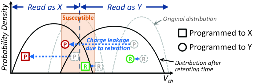
Figure 5 shows how the threshold voltage of a retention-prone cell (i.e., a fast-leaking cell, labeled P in the figure) decreases over time (i.e., the cell shifts to the left) due to retention leakage, while the threshold voltage of a retention- resistant cell (i.e., a slow-leaking cell, labeled R in the figure) does not change significantly over time. Retention Failure Recovery (RFR) uses this classification of retention-prone versus retention-resistant cells to correct the data from the failed page without the assistance of ECC. Without loss of generality, let us assume that we are studying susceptible cells near the intersection of two threshold voltage distributions X and Y, where Y contains higher voltages than X. Figure 5 highlights the region of cells considered susceptible by RFR using a box, labeled Susceptible. A susceptible cell within the box that is retention prone likely belongs to distribution Y, as a retention-prone cell shifts rapidly to a lower voltage (see the circled cell labeled P within the susceptible region in the figure). A retention-resistant cell in the same susceptible region likely belongs to distribution X (see the boxed cell labeled R within the susceptible region in the figure).
RFR identifies fast- vs. slow-leaking cells, and uses selective bit flipping to correct retention failures, thus reducing RBER. With reduced raw bit errors, the read data may be reconstructed by ECC with a higher probability. RFR consists of the following four offline steps, which are triggered when an uncorrectable error is found:
-
•
Step 1: Identify data with a retention failure. Once the flash controller fails to read a flash page, a retention failure is identified on that page.
-
•
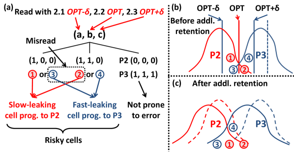
Step 2: Identify susceptible cells using three read operations. We read the failed page using three read reference voltages: OPT (the optimal read reference voltage) minus some margin (Step 2.1), OPT (Step 2.2), and OPT plus (Step 2.3). The value of is large enough to include the entire Susceptible region shown in Figure 5. Figure 6a illustrates the identification of susceptible (i.e., risky) cells, which are denoted as type ①, type ②, type ③, and type ④ cells.
-
•
Step 3: Identify fast- and slow-leaking cells. We compare the threshold voltage of susceptible cells before and after several days of retention to classify them as fast- and slow-leaking cells. Figures 6b and 6c illustrate how the cells shift differently after additional retention loss. Among the susceptible cells, type ① and type ② cells are slow-leaking cells, whereas type ③ and type ④ cells are fast-leaking cells.
-
•
Step 4: Selectively flip bits based on the identification results from Step 3. Using the leakage speed information, we now know that type ② and type ③ cells are likely misread. Thus, we simply flip those cells to correct these likely errors.
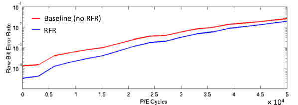
We evaluate RFR on data programmed to random values that has 28-day equivalent retention age. In Step 3, we introduce an additional 12 days’ worth of equivalent retention age. Figure 7 shows the resulting raw bit error rate of RFR over a range of P/E cycles (compared to that of the baseline). This figure shows that RFR reduces the RBER by 50%, averaged across all evaluated wearout levels (P/E cycles). Thus, we expect the number of raw bit errors to be halved, increasing the chances that these errors are correctable by ECC.
5 Related Work
To our knowledge, our HPCA 2015 paper [10] is the first to 1) experimentally characterize and comprehensively analyze how the threshold voltage distribution changes over different retention ages, as well as the implication of these changes on the read reference voltage and lifetime, using real state-of-the-art 2Y-nm MLC NAND flash memory chips; and 2) proposes two novel techniques to mitigate the impact of retention age online and to recover from data loss by exploiting retention behavior. In this section, we briefly discuss various related works.
5.1 Works on NAND Flash Memory
NAND Flash Memory Retention Error Characterization. Multiple prior works characterize NAND flash data retention, but mainly in terms of RBER [8, 12, 13, 80]. These works show that 1) retention errors are the dominant errors in NAND flash memory, and 2) the retention error rate increases with the retention age and the P/E cycle. Papandreou et al. [91] characterize the retention effect on threshold voltage distributions under high temperature baking, and find that the distribution shifts to lower voltage over retention time, and so does the optimal read reference voltage. In contrast, our HPCA 2015 paper [10] characterizes data retention under room temperature, which is closer to how NAND flash memories are typically used [10]. Our recent work characterizes how data retention affects the threshold voltage distribution for TLC NAND flash memory [3, 4, 5], making similar findings as our HPCA 2015 paper [10].
NAND Flash Memory Error Characterization. Prior works study different types of NAND flash memory errors in MLC, planar NAND flash memory, including P/E cycling errors [80, 9, 93, 71, 91], programming errors [6, 93, 71], cell-to-cell program interference errors [11, 9, 14], retention errors [80, 9, 12, 10, 91], and read disturb errors [80, 15, 91]. These works characterize how raw bit error rate and threshold voltage distributions change with various types of noise. Our recent work characterizes the same types of errors in planar TLC NAND flash memory and has similar findings [3, 4, 5]. Thus, we believe that most of the findings on MLC NAND flash memory can be generalized to any types of planar NAND flash memory devices (e.g., SLC, MLC, TLC, or QLC). Recent works [77, 89, 101] have also studied SSD errors in the field, and have shown the system-level implications of these errors in large-scale data centers. Unlike our characterization, these in-the-field studies do not have access to the underlying NAND flash memory within the SSDs that they test, and, thus, are unable to show detailed data retention behavior.
3D NAND Flash Memory Error Characterization. Recently, manufacturers have begun to produce SSDs that contain three-dimensional (3D) NAND flash memory [117, 92, 42, 36, 79, 78]. In 3D NAND flash memory, multiple layers of flash cells are stacked vertically to increase the density and to improve the scalability of the memory [117]. In order to achieve this stacking, manufacturers have changed a number of underlying properties of the flash memory design. We refer readers to our prior work for a detailed comparison between 3D NAND flash memory and planar NAND flash memory [3, 4, 5]. Previous works [82, 22] compare the retention loss between 3D charge trap NAND flash memory and planar NAND flash memory through real device characterization, and find that 3D charge trap cells leak charge faster than planar NAND cells and thus experience the phenomenon of early retention loss. Our recent work [72] characterizes the impact of dwell time, i.e., the idle time between consecutive program cycles, and environmental temperature on the retention loss speed and program variation of 3D charge trap NAND flash memory, and proposes techniques to mitigate these issues to improve flash memory lifetime. Recent work [113] characterizes the latency and raw bit error rate of 3D NAND flash memory devices based on floating gate cells, and makes similar observations as those for planar NAND flash memory devices based on floating gate cells. Prior works have reported several differences between 3D NAND and planar NAND through circuit level measurements, including the fact that 3D NAND flash cells exhibit 1) smaller program variation at high P/E cycle [92], 2) smaller program interference [92], and 3) early retention loss [22, 82, 22]. The field (both academia and industry) is currently in much need of detailed rigorous experimental characterization and analysis of state-of-the-art 3D NAND flash memory devices.
Retention Error Mitigation Using Periodic Refresh. Prior works [12, 13, 69, 90] propose to use periodic refresh to mitigate retention errors. Cai et al. [12, 13] introduce 1) remapping-based refresh, which periodically reads data from each valid flash block, corrects any data errors, and remaps the data to a different physical location, 2) in-place refresh, which incrementally replenishes the lost charge of each page at its current location, and 3) adaptive refresh, which allows the controller to adaptively adjust the rate that the refresh mechanisms are invoked based on the wearout (i.e., the current P/E cycle count) of the NAND flash memory [12, 13]; or the temperature of the SSD [8, 10]. However, these techniques 1) require the system to be consistently powered on, and 2) are unaware of the fact that the optimal read reference voltage changes with different retention age. Note that these works always apply a fixed read reference voltage regardless of the retention age of the cell, which is suboptimal for reading flash blocks at different retention ages. In contrast, our ROR technique optimizes the read reference voltage of each flash block based on its retention age, leading to significant lifetime improvements. Several works [70, 23, 104] find that refresh operations consume a large number of P/E cycles, and propose techniques that exploit workload write-hotness to relax the guaranteed retention time of NAND flash memory without requiring refresh. For example, WARM [70] partitions write-hot and write-cold data using a lightweight mechanism designed for flash memory, and eliminates the need to refresh write-hot data, leading to significant lifetime improvements over existing periodic refresh mechanisms. Our techniques can be combined with such refresh elimination techniques for higher lifetime and performance.
Read Reference Voltage Optimization. A few works [91, 11, 14] propose optimizing the read reference voltage. Cai et al. [14] propose a technique to calculate the optimal read reference voltage from the mean and variance of the threshold voltage distributions, which are characterized by the read-retry technique [9]. The cost of such a technique is relatively high, as it requires periodically reading flash memory with all possible read reference voltages to discover the threshold voltage distributions. Papandreou et al. [91] propose to apply a per-block close-to-optimal read reference voltage by periodically sampling and averaging 6 OPTs within each block, learned by exhaustively trying all possible read reference voltages. In contrast, ROR can find the actual optimal read reference voltage at a much lower latency, thanks to the new findings and observations in our HPCA 2015 paper [10]. We show that ROR greatly outperforms naive read-retry. The latter is significantly simpler than the mechanism proposed in [91].
Recently, Luo et al. [71] propose to accurately predict the optimal read reference voltage using an online flash channel model for each chip learned online. Cai et al. [15] propose a new technique called tuning, which tunes the pass-through voltage, i.e., a high reference voltage applied to turn on unread cells in a block, to mitigate read disturb errors. Du et al. [27] propose to tune the optimal read reference voltages for ECC soft decoding to improve the ECC correction capability (i.e., the maximum number of errors that ECC can correct). Fukami et al. [28] propose to use read-retry to improve the reliability of the chip-off forensic analysis of NAND flash memory devices. Our proposals are complementary to all these techniques.
Error Recovery. To our knowledge, our HPCA 2015 paper [10] proposes the first mechanism that can recover data even after ECC is unable to successfully correct all of the errors due to retention loss. One of our works [15] builds on our HPCA 2015 paper and adapts the RFR mechanism to opportunistically recover from read disturb errors instead of retention errors. FlashDefibrillator (FD) [39] improves upon RFR to recover from data retention errors online. FD recovers data retention errors online by applying a sequence of diagnostic pulses that recharge the fast-leaking cells. This helps recover otherwise uncorrectable errors in two ways: (1) fast-leaking cells may be recharged back to the correct state, (2) fast-leaking cells recharge faster than slow-leaking cells, thus fast-leaking cells can be identified as the cells whose threshold voltages increase faster during the diagnostic pulses. These two more recent works [15, 39] directly build upon our HPCA 2015 paper.
5.2 Data Retention Errors in DRAM
DRAM uses the charge within a capacitor to represent one bit of data. Much like the floating gate within NAND flash memory, charge leaks from the DRAM capacitor over time, leading to data retention issues. Unlike a NAND flash cell, where leakage typically leads to data loss after several days to years of retention time, leakage from a DRAM cell leads to data loss after a retention time on the order of milliseconds to seconds [67].
The retention time of a DRAM cell depends upon several factors [67], including (1) manufacturing process variation and (2) temperature. Manufacturing process variation affects the amount of current that leaks from each DRAM cell’s capacitor and access transistor [67]. As a result, the retention time of the cells within a single DRAM chip vary significantly, resulting in strong cells that have high retention times and weak cells that have low retention times within each chip. The operating temperature affects the rate at which charge leaks from the capacitor. As the operating temperature increases, the retention time of a DRAM cell decreases exponentially [67, 29].
Due to the rapid charge leakage from DRAM cells, a DRAM controller periodically refreshes all DRAM cells in place [68, 17, 67, 38, 97, 44, 94] (similar to the periodic refresh techniques used in NAND flash memory, but at a much smaller time scale). DRAM standards require a DRAM cell to be refreshed once every [38]. As the density of DRAM continues to increase over successive product generations (e.g., by 128x between 1999 and 2017 [18, 16]), enabled by the scaling of DRAM to smaller manufacturing process technology nodes [73, 87, 85, 84], the performance and energy overheads required to refresh an entire DRAM module have grown significantly [84, 68, 17, 87, 85]. It is expected that the refresh problem will get significantly worse and limit DRAM density scaling, as described in a recent work by Samsung and Intel [43] and by our group [68]. Prior analysis shows that when DRAM chip density reaches , nearly 50% of the data throughput is lost due to the high amount of time spent on refreshing all of the rows in the chip, and nearly 50% of the DRAM chip power is spent on refresh operations [68]. Thus, data retention problems and refresh pose a clear challenge to DRAM scalability.
Various experimental studies of real DRAM chips (e.g., [68, 67, 62, 97, 44, 45, 94, 50, 32]) have studied the data retention time of DRAM cells in modern chips, and have shown that the vast majority of DRAM cells can retain data without loss for much longer than the retention time specified by DRAM standards. A number of works take advantage of this variability in data retention time behavior across DRAM cells, by reducing the frequency at which the vast majority of DRAM rows within a module are refreshed (e.g., [68, 67, 97, 44, 110, 37, 94, 46, 2]), or by reducing the interference caused by refresh requests on demand requests (e.g., [17, 83, 108]).
More findings on the nature of DRAM data retention and associated errors, as well as relevant experimental data from modern DRAM chips, can be found in our prior works [68, 17, 67, 62, 97, 44, 45, 94, 32, 16, 47, 46, 84]. We also refer the readers to prior works on the design and operation of the underlying DRAM architecture [53, 54, 51, 63, 62, 33, 68, 17, 19, 103, 20, 60, 102, 67, 18, 32, 55, 64, 61, 52, 94, 49].
5.3 Errors in Emerging Nonvolatile Memory Technologies
DRAM operations are several orders of magnitude faster than SSD operations, but DRAM has two major disadvantages. First, DRAM offers orders of magnitude less storage density than NAND-flash-memory-based SSDs. Second, DRAM is volatile (i.e., the stored data is lost on a power outage). Emerging nonvolatile memories, such as phase-change memory (PCM) [57, 98, 112, 59, 121, 58, 115, 76], spin-transfer torque magnetic RAM (STT-RAM or STT-MRAM) [88, 56], metal-oxide resistive RAM (RRAM) [111], and memristors [26, 107], are expected to bridge the gap between DRAM and SSDs, providing DRAM-like access latency and energy, and at the same time SSD-like large capacity and nonvolatility (and hence SSD-like data persistence). These technologies are also expected to be used as part of hybrid memory systems (also called heterogeneous memory systems), where one part of the memory consists of DRAM modules and another part consists of modules of emerging technologies [98, 115, 100, 116, 99, 119, 75, 65, 74, 118, 25, 24, 41, 95, 21].
PCM-based devices are expected to have a limited lifetime, as PCM can only endure a certain number of writes [57, 98, 112], similar to the P/E cycling errors in NAND-flash-memory-based SSDs (though PCM’s write endurance is higher than that of SSDs). PCM suffers from (1) resistance drift [112, 96, 35], where the resistance used to represent the value becomes higher over time (and eventually can introduce a bit error), similar to how charge leakage in NAND flash memory and DRAM lead to retention errors over time; and (2) write disturb [40], where the heat generated during the programming of one PCM cell dissipates into neighboring cells and can change the value that is stored within the neighboring cells. STT-RAM suffers from (1) retention failures, where the value stored for a single bit (as the magnetic orientation of the layer that stores the bit) can flip over time; and (2) read disturb (a conceptually different phenomenon from the read disturb in DRAM and flash memory), where reading a bit in STT-RAM can inadvertently induce a write to that same bit [88].
Due to the nascent nature of emerging nonvolatile memory technologies and the lack of availability of large-capacity devices built with them, extensive and dependable experimental studies have yet to be conducted on the reliability of real PCM, STT-RAM, RRAM, and memristor chips. However, we believe that error mechanisms conceptually or abstractly similar to those we discussed for flash memory and DRAM are likely to be prevalent in emerging technologies as well (as supported by some recent studies [88, 40, 120, 48, 1, 105, 106]), albeit with different underlying mechanisms and error rates. We expect that the ROR and RFR techniques we propose in our HPCA 2015 paper [10] can be easily adapted to NVM technologies.
6 Significance
Our HPCA 2015 paper [10] provides extensive characterization data and proposes novel mechanisms to mitigate retention errors in modern NAND flash memory and recover data when ECC fails. We believe that our characterization and mechanisms will have a significant impact on the community, as evidenced by multiple recent works directly building upon our HPCA 2015 paper [15, 39, 72].
6.1 Long-Term Impact
We believe our work will have long-term impact for the following three reasons. First, as NAND flash memory becomes denser in the future, data retention will become a bigger issue, and thus a better understanding of its implication and characteristics will be important to help maintain NAND flash reliability after scaling [84, 3, 4, 5]. Second, we propose an online technique that reduces flash read latency, and we give insights into the flash read-retry algorithm, thereby hopefully inspiring future works to further optimize flash read latency. Third, we propose an offline technique that leverages underlying flash characteristics to enable recovery from a retention failure even after the drive fails to correct it, thereby hopefully inspiring future works to look for more ways to prevent data loss.
Data Retention. Our work provides a comprehensive analysis of the retention loss effect on real NAND flash memory chips, which enhances the understanding of the retention loss effect in the research community. We hope that our analysis and solutions can inspire more works to handle data retention in better ways. As planar NAND flash memory becomes denser, each flash memory cell holds less charge and becomes more vulnerable to retention loss [8, 12]. Thus, in the future, we expect data retention to become a more important problem [84, 3, 4, 5], and expect that industry will be more open to adapt new solutions like our proposals, ROR and RFR. In fact, several flash-based SSDs currently use refresh as a solution to mitigate retention errors [31, 34, 114]. Our work shows that we can go significantly beyond refresh to tolerate the data retention problem in NAND flash memory.
Read Performance Optimization. The read performance advantage of flash memory over hard disk drives makes flash-based SSDs more appealing than hard disk drives. However, many existing solutions, such as read-retry [9, 28], trade off flash performance for reliability. Our HPCA 2015 paper [10] is the first to point out the read performance problem, and to provide a detailed analysis and new solution to this problem. We hope that our work can enhance the research community’s understanding of flash read performance and bring more attention to flash read performance, which is critically important to overall system performance. Techniques that are developed in DRAM to reduce read latency [53, 54, 51, 63, 62, 33, 68, 17, 19, 103, 20, 60, 102, 18, 64, 61, 52, 94] can prompt inspiration for NAND flash memory.
Data Recovery. Prior to our work, after a retention failure happens, an uncorrectable error and resulting data corruption was considered to be unrecoverable from, resulting in data loss. To our knowledge, our HPCA 2015 paper [10] is the first to show that it is actually possible to recover this data using our RFR mechanism. As the reliability of NAND flash memory decreases, and the popularity of flash-based SSDs increases, SSD failures are expected to increase, creating a greater need for recovery techniques that can retrieve previously-unrecoverable data. In light of this, recent works [15, 39] have directly built upon RFR to provide additional data recovery mechanisms. We hope that our work draws more attention to flash memory data recovery, and inspires further solutions to this important problem.
6.2 New Research Directions
Our HPCA 2015 paper [10] presents characterization results for data retention in real NAND flash chips. By making such data and knowledge available, we believe that the flash memory and SSD research communities can have a better understanding of data retention, and can therefore develop better solutions to tackle the retention problem in the future. We hope that our work will continue to inspire future works in flash memory that can provide a comprehensive characterization and analysis of other NAND flash memory behavior using real chips, such as program/erase cycling and cell-to-cell program disturbance. We also hope that our ROR and RFR techniques bring more attention to both the flash read performance problem and data recovery problem, and that they will inspire researchers from both academia and industry to develop and adopt new solutions.
7 Conclusion
Our HPCA 2015 paper [10] comprehensively characterizes and analyzes how the threshold voltage distribution and the optimal read reference voltages of state-of-the-art 2Y-nm MLC NAND flash memory change over different retention ages. Based on these analyses, the paper proposes two new techniques. Retention Optimized Reading (ROR) improves reliability, lifetime, and performance of MLC NAND flash memory at modest storage cost by optimizing the read reference voltage of each flash memory block based on its retention age. We demonstrate significant benefits with ROR in terms of reduced RBER, extended flash lifetime, and reduction in flash read latency. Retention Failure Recovery (RFR) recovers data with uncorrectable errors by identifying and probabilistically correcting flash cells with retention errors. We demonstrate large raw bit error rate reductions with RFR. We hope that our comprehensive characterization of data retention in flash memory will enable better understanding of flash retention errors and motivate other new techniques to overcome these errors. We believe the importance of our two new techniques (ROR and RFR) will grow as NAND flash memory scales to smaller feature sizes and becomes even less reliable in the future.
Acknowledgments
We thank Nandita Vijaykumar and the anonymous reviewers for feedback. This work is partially supported by the Intel Science and Technology Center, CMU Data Storage Systems Center, and NSF grants 1212962 and 1320531.
References
- [1] A. Athmanathan, M. Stanisavljevic, N. Papandreou, H. Pozidis, and E. Eleftheriou, “Multilevel-Cell Phase-Change Memory: A Viable Technology,” JETCAS, 2016.
- [2] S. Baek, S. Cho, and R. Melhem, “Refresh Now and Then,” IEEE Trans. Computers, Aug. 2014.
- [3] Y. Cai, S. Ghose, E. F. Haratsch, Y. Luo, and O. Mutlu, “Error Characterization, Mitigation, and Recovery in Flash-Memory-Based Solid-State Drives,” Proc. IEEE, Sep. 2017.
- [4] Y. Cai, S. Ghose, E. F. Haratsch, Y. Luo, and O. Mutlu, “Error Characterization, Mitigation, and Recovery in Flash Memory Based Solid-State Drives,” arXiv:1706.08642 [cs.AR], 2017.
- [5] Y. Cai, S. Ghose, E. F. Haratsch, Y. Luo, and O. Mutlu, “Errors in Flash-Memory-Based Solid-State Drives: Analysis, Mitigation, and Recovery,” arXiv:1711.11427 [cs.AR], 2017.
- [6] Y. Cai, S. Ghose, Y. Luo, K. Mai, O. Mutlu, and E. F. Haratsch, “Vulnerabilities in MLC NAND Flash Memory Programming: Experimental Analysis, Exploits, and Mitigation Techniques,” in HPCA, 2017.
- [7] Y. Cai, E. F. Haratsch, M. P. McCartney, and K. Mai, “FPGA-Based Solid-State Drive Prototyping Platform,” in FCCM, 2011.
- [8] Y. Cai, E. F. Haratsch, O. Mutlu, and K. Mai, “Error Patterns in MLC NAND Flash Memory: Measurement, Characterization, and Analysis,” in DATE, 2012.
- [9] Y. Cai, E. F. Haratsch, O. Mutlu, and K. Mai, “Threshold Voltage Distribution in NAND Flash Memory: Characterization, Analysis, and Modeling,” in DATE, 2013.
- [10] Y. Cai, Y. Luo, E. F. Haratsch, K. Mai, and O. Mutlu, “Data Retention in MLC NAND Flash Memory: Characterization, Optimization, and Recovery,” in HPCA, 2015.
- [11] Y. Cai, O. Mutlu, E. F. Haratsch, and K. Mai, “Program Interference in MLC NAND Flash Memory: Characterization, Modeling, and Mitigation,” in ICCD, 2013.
- [12] Y. Cai, G. Yalcin, O. Mutlu, E. F. Haratsch, A. Cristal, O. Unsal, and K. Mai, “Flash Correct and Refresh: Retention Aware Management for Increased Lifetime,” in ICCD, 2012.
- [13] Y. Cai, G. Yalcin, O. Mutlu, E. F. Haratsch, A. Cristal, O. Unsal, and K. Mai, “Error Analysis and Retention-Aware Error Management for NAND Flash Memory,” Intel Technology Journal, 2013.
- [14] Y. Cai, G. Yalcin, O. Mutlu, E. F. Haratsch, O. Unsal, A. Cristal, and K. Mai, “Neighbor Cell Assisted Error Correction in MLC NAND Flash Memories,” in SIGMETRICS, 2014.
- [15] Y. Cai, Y. Luo, S. Ghose, E. F. Haratsch, K. Mai, and O. Mutlu, “Read Disturb Errors in MLC NAND Flash Memory: Characterization, Mitigation, and Recovery,” in DSN, 2015.
- [16] K. K. Chang, “Understanding and Improving the Latency of DRAM-Based Memory Systems,” Ph.D. dissertation, Carnegie Mellon Univ., 2017.
- [17] K. K. Chang, D. Lee, Z. Chishti, A. Alameldeen, C. Wilkerson, Y. Kim, and O. Mutlu, “Improving DRAM Performance by Parallelizing Refreshes With Accesses,” in HPCA, 2014.
- [18] K. K. Chang, A. Kashyap, H. Hassan, S. Ghose, K. Hsieh, D. Lee, T. Li, G. Pekhimenko, S. Khan, and O. Mutlu, “Understanding Latency Variation in Modern DRAM Chips: Experimental Characterization, Analysis, and Optimization,” in SIGMETRICS, 2016.
- [19] K. K. Chang, P. J. Nair, D. Lee, S. Ghose, M. K. Qureshi, and O. Mutlu, “Low-Cost Inter-Linked Subarrays (LISA): Enabling Fast Inter-Subarray Data Movement in DRAM,” in HPCA, 2016.
- [20] K. K. Chang, A. G. Yaglikci, A. Agrawal, N. Chatterjee, S. Ghose, A. Kashyap, H. Hassan, D. Lee, M. O’Connor, and O. Mutlu, “Understanding Reduced-Voltage Operation in Modern DRAM Devices: Experimental Characterization, Analysis, and Mechanisms,” in SIGMETRICS, 2017.
- [21] N. Chatterjee, M. Shevgoor, R. Balasubramonian, A. Davis, Z. Fang, R. Illikkal, and R. Iyer, “Leveraging Heterogeneity in DRAM Main Memories to Accelerate Critical Word Access,” in MICRO, 2012.
- [22] B. Choi et al., “Comprehensive Evaluation of Early Retention (Fast Charge Loss Within a Few Seconds) Characteristics in Tube-Type 3-D NAND Flash Memory,” in VLSIT, 2016.
- [23] W. Choi, M. Arjomand, M. Jung, and M. Kandemir, “Exploiting Data Longevity for Enhancing the Lifetime of Flash-based Storage Class Memory,” in SIGMETRICS, 2017.
- [24] C.-C. Chou, A. Jaleel, and M. K. Qureshi, “CAMEO: A Two-Level Memory Organization with Capacity of Main Memory and Flexibility of Hardware-Managed Cache,” in MICRO, 2014.
- [25] C.-C. Chou, A. Jaleel, and M. K. Qureshi, “BEAR: Techniques for Mitigating Bandwidth Bloat in Gigascale DRAM Caches,” in ISCA, 2015.
- [26] L. Chua, “Memristor—The Missing Circuit Element,” TCT, 1971.
- [27] Y. Du, Q. Li, L. Shi, D. Zou, H. Jin, and C. J. Xue, “Reducing LDPC Soft Sensing Latency by Lightweight Data Refresh for Flash Read Performance Improvement,” in DAC, 2017.
- [28] A. Fukami, S. Ghose, Y. Luo, Y. Cai, and O. Mutlu, “Improving the Reliability of Chip-Off Forensic Analysis of NAND Flash Memory Devices,” Digital Investigation, 2017.
- [29] T. Hamamoto, S. Sugiura, and S. Sawada, “On the Retention Time Distribution of Dynamic Random Access Memory (DRAM),” IEEE Trans. Electron Devices, Jun. 1998.
- [30] R. W. Hamming, “Error Detecting and Error Correcting Codes,” Bell Labs Technical Journal, 1950.
- [31] P. Hansson, “When SSD Performance Goes Awry,” http://www.techspot.com/article/997-samsung-ssd-read-performance-degradation/, 2015.
- [32] H. Hassan, N. Vijaykumar, S. Khan, S. Ghose, K. Chang, G. Pekhimenko, D. Lee, O. Ergin, and O. Mutlu, “SoftMC: A Flexible and Practical Open-Source Infrastructure for Enabling Experimental DRAM Studies,” in HPCA, 2017.
- [33] H. Hassan, G. Pekhimenko, N. Vijaykumar, V. Seshadri, D. Lee, O. Ergin, and O. Mutlu, “ChargeCache: Reducing DRAM Latency by Exploiting Row Access Locality,” in HPCA, 2016.
- [34] G. Hippo, “Hippotizer V4,” http://cdn.manula.com/user/8056/9036_9608_en_1479375721.pdf?v=20170201164158, 2017.
- [35] D. Ielmini, A. L. Lacaita, and D. Mantegazza, “Recovery and Drift Dynamics of Resistance and Threshold Voltages in Phase-Change Memories,” TED, 2007.
- [36] J. Im et al., “A 128Gb 3b/Cell V-NAND Flash Memory with 1Gb/s I/O Rate,” in ISSCC, 2015.
- [37] C. Isen and L. John, “ESKIMO — Energy Savings Using Semantic Knowledge of Inconsequential Memory Occupancy for DRAM Subsystem,” in MICRO, 2009.
- [38] JEDEC Solid State Technology Assn., DDR4 SDRAM Standard, Publication JESD79-4A, 2013.
- [39] J. Jeong, Y. Song, and J. Kim, “FlashDefibrillator: A Data Recovery Technique for Retention Failures in NAND Flash Memory,” in NVMSA, 2015.
- [40] L. Jiang, Y. Zhang, and J. Yang, “Mitigating Write Disturbance in Super-Dense Phase Change Memories,” in DSN, 2014.
- [41] X. Jiang, N. Madan, L. Zhao, M. Upton, R. Iyer, S. Makineni, D. Newell, D. Solihin, and R. Balasubramonian, “CHOP: Adaptive Filter-Based DRAM Caching for CMP Server Platforms,” in HPCA, 2010.
- [42] D. Kang et al., “7.1 256Gb 3b/cell V-NAND Flash Memory With 48 Stacked WL Layers,” in ISSCC, 2016.
- [43] U. Kang, H.-S. Yu, C. Park, H. Zheng, J. Halbert, K. Bains, S. Jang, and J. Choi, “Co-Architecting Controllers and DRAM to Enhance DRAM Process Scaling,” in Memory Forum, 2014.
- [44] S. Khan, D. Lee, Y. Kim, A. Alameldeen, C. Wilkerson, and O. Mutlu, “The Efficacy of Error Mitigation Techniques for DRAM Retention Failures: A Comparative Experimental Study,” in SIGMETRICS, 2014.
- [45] S. Khan, D. Lee, and O. Mutlu, “PARBOR: An Efficient System-Level Technique to Detect Data-Dependent Failures in DRAM,” in DSN, 2016.
- [46] S. Khan, C. Wilkerson, D. Lee, A. R. Alameldeen, and O. Mutlu, “A Case for Memory Content-Based Detection and Mitigation of Data-Dependent Failures in DRAM,” IEEE Comput. Archit. Lett., 2016.
- [47] S. Khan, C. Wilkerson, Z. Wang, A. R. Alameldeen, D. Lee, and O. Mutlu, “Detecting and Mitigating Data-Dependent DRAM Failures by Exploiting Current Memory Content,” in MICRO, 2017.
- [48] W.-S. Khwa et al., “A Resistance-Drift Compensation Scheme to Reduce MLC PCM Raw BER by Over 100x for Storage-Class Memory Applications,” in ISSCC, 2016.
- [49] J. S. Kim, M. Patel, H. Hassan, and O. Mutlu, “The DRAM Latency PUF: Quickly Evaluating Physical Unclonable Functions by Exploiting the Latency–Reliability Tradeoff in Modern DRAM Devices,” in HPCA, 2018.
- [50] K. Kim and J. Lee, “A New Investigation of Data Retention Time in Truly Nanoscaled DRAMs,” IEEE Electron Device Lett., Aug. 2009.
- [51] Y. Kim, V. Seshadri, D. Lee, J. Liu, and O. Mutlu, “A Case for Exploiting Subarray-Level Parallelism (SALP) in DRAM,” in ISCA, 2012.
- [52] Y. Kim, R. Daly, J. Kim, C. Fallin, J. H. Lee, D. Lee, C. Wilkerson, K. Lai, and O. Mutlu, “Flipping Bits in Memory Without Accessing Them: An Experimental Study of DRAM Disturbance Errors,” in ISCA, 2014.
- [53] Y. Kim, D. Han, O. Mutlu, and M. Harchol-Balter, “ATLAS: A Scalable and High-Performance Scheduling Algorithm for Multiple Memory Controllers,” in HPCA, 2010.
- [54] Y. Kim, M. Papamichael, O. Mutlu, and M. Harchol-Balter, “Thread Cluster Memory Scheduling: Exploiting Differences in Memory Access Behavior,” in MICRO, 2010.
- [55] Y. Kim, W. Yang, and O. Mutlu, “Ramulator: A Fast and Extensible DRAM Simulator,” CAL, 2015.
- [56] E. Kültürsay, M. Kandemir, A. Sivasubramaniam, and O. Mutlu, “Evaluating STT-RAM as an Energy-Efficient Main Memory Alternative,” in ISPASS, 2013.
- [57] B. C. Lee, E. Ipek, O. Mutlu, and D. Burger, “Architecting Phase Change Memory as a Scalable DRAM Alternative,” in ISCA, 2009.
- [58] B. C. Lee, E. Ipek, O. Mutlu, and D. Burger, “Phase Change Memory Architecture and the Quest for Scalability,” Commun. ACM, Jul. 2010.
- [59] B. C. Lee, P. Zhou, J. Yang, Y. Zhang, B. Zhao, E. Ipek, O. Mutlu, and D. Burger, “Phase-Change Technology and the Future of Main Memory,” IEEE Micro, Feb. 2010.
- [60] D. Lee, S. Khan, L. Subramanian, S. Ghose, R. Ausavarungnirun, G. Pekhimenko, V. Seshadri, and O. Mutlu, “Design-Induced Latency Variation in Modern DRAM Chips: Characterization, Analysis, and Latency Reduction Mechanisms,” in SIGMETRICS, 2017.
- [61] D. Lee, S. Ghose, G. Pekhimenko, S. Khan, and O. Mutlu, “Simultaneous Multi-Layer Access: Improving 3D-Stacked Memory Bandwidth at Low Cost,” TACO, 2016.
- [62] D. Lee, Y. Kim, G. Pekhimenko, S. Khan, V. Seshadri, K. Chang, and O. Mutlu, “Adaptive-Latency DRAM: Optimizing DRAM Timing for the Common-Case,” in HPCA, 2015.
- [63] D. Lee, Y. Kim, V. Seshadri, J. Liu, L. Subramanian, and O. Mutlu, “Tiered-Latency DRAM: A Low Latency and Low Cost DRAM Architecture,” in HPCA, 2013.
- [64] D. Lee, L. Subramanian, R. Ausavarungnirun, J. Choi, and O. Mutlu, “Decoupled Direct Memory Access: Isolating CPU and IO Traffic by Leveraging a Dual-Data-Port DRAM,” in PACT, 2015.
- [65] Y. Li, S. Ghose, J. Choi, J. Sun, H. Wang, and O. Mutlu, “Utility-Based Hybrid Memory Management,” in CLUSTER, 2017.
- [66] S. Lin and D. J. Costello, Error Control Coding. Prentice Hall, 2004.
- [67] J. Liu, B. Jaiyen, Y. Kim, C. Wilkerson, and O. Mutlu, “An Experimental Study of Data Retention Behavior in Modern DRAM Devices: Implications for Retention Time Profiling Mechanisms,” in ISCA, 2013.
- [68] J. Liu, B. Jaiyen, R. Veras, and O. Mutlu, “RAIDR: Retention-Aware Intelligent DRAM Refresh,” in ISCA, 2012.
- [69] R.-S. Liu, C.-L. Yang, and W. Wu, “Optimizing NAND Flash-Based SSDs via Retention Relaxation,” in FAST, 2012.
- [70] Y. Luo, Y. Cai, S. Ghose, J. Choi, and O. Mutlu, “WARM: Improving NAND Flash Memory Lifetime With Write-Hotness Aware Retention Management,” in MSST, 2015.
- [71] Y. Luo, S. Ghose, Y. Cai, E. F. Haratsch, and O. Mutlu, “Enabling Accurate and Practical Online Flash Channel Modeling for Modern MLC NAND Flash Memory,” JSAC, 2016.
- [72] Y. Luo, S. Ghose, Y. Cai, E. F. Haratsch, and O. Mutlu, “HeatWatch: Improving 3D NAND Flash Memory Device Reliability by Exploiting Self-Recovery and Temperature Awareness,” in HPCA, 2018.
- [73] J. A. Mandelman, R. H. Dennard, G. B. Bronner, J. K. DeBrosse, R. Divakaruni, Y. Li, and C. J. Radens, “Challenges and Future Directions for the Scaling of Dynamic Random-Access Memory (DRAM),” IBM J. Research Develop., Mar. 2002.
- [74] J. Meza, Y. Luo, S. Khan, J. Zhao, Y. Xie, and O. Mutlu, “A Case for Efficient Hardware-Software Cooperative Management of Storage and Memory,” in WEED, 2013.
- [75] J. Meza, J. Chang, H. Yoon, O. Mutlu, and P. Ranganathan, “Enabling Efficient and Scalable Hybrid Memories Using Fine-Granularity DRAM Cache Management,” IEEE Comput. Archit. Lett., Feb. 2012.
- [76] J. Meza, J. Li, and O. Mutlu, “Evaluating Row Buffer Locality in Future Non-Volatile Main Memories,” Carnegie Mellon Univ., SAFARI Research Group, Tech. Rep. TR-SAFARI-2012-002, 2012.
- [77] J. Meza, Q. Wu, S. Kumar, and O. Mutlu, “A Large-Scale Study of Flash Memory Failures In The Field,” in SIGMETRICS, 2015.
- [78] R. Micheloni, Ed., 3D Flash Memories. Dordrecht, Netherlands: Springer Netherlands, 2016.
- [79] R. Micheloni, S. Aritome, and L. Crippa, “Array Architectures for 3-D NAND Flash Memories,” Proc. IEEE, Sep. 2017.
- [80] N. Mielke, T. Marquart, N.Wu, J.Kessenich, H. Belgal, E. Schares, and F. Triverdi, “Bit Error Rate in NAND Flash Memories,” in IRPS, 2008.
- [81] I. Min, “Enterprise NAND Flash Memory with 1x-nm Technology,” in FMS, 2014.
- [82] K. Mizoguchi, T. Takahashi, S. Aritome, and K. Takeuchi, “Data-Retention Characteristics Comparison of 2D and 3D TLC NAND Flash Memories,” in IMW, 2017.
- [83] J. Mukundan, H. Hunter, K.-H. Kim, J. Stuecheli, and J. F. Martínez, “Understanding and Mitigating Refresh Overheads in High-Density DDR4 DRAM Systems,” in ISCA, 2013.
- [84] O. Mutlu, “The RowHammer Problem and Other Issues We May Face as Memory Becomes Denser,” in DATE, 2017.
- [85] O. Mutlu, “Memory Scaling: A Systems Architecture Perspective,” in IMW, 2013.
- [86] O. Mutlu, “Error Analysis and Management for MLC NAND Flash Memory,” in FMS, 2014.
- [87] O. Mutlu and L. Subramanian, “Research Problems and Opportunities in Memory Systems,” SUPERFRI, 2014.
- [88] H. Naeimi, C. Augustine, A. Raychowdhury, S.-L. Lu, and J. Tschanz, “STT-RAM Scaling and Retention Failure,” Intel Technology Journal, 2013.
- [89] I. Narayanan, D. Wang, M. Jeon, B. Sharma, L. Caulfield, A. Sivasubramaniam, B. Cutler, J. Liu, B. Khessib, and K. Vaid, “SSD Failures in Datacenters: What? When? and Why?” in SYSTOR, 2016.
- [90] Y. Pan, G. Dong, Q. Wu, and T. Zhang, “Quasi-Nonvolatile SSD: Trading Flash Memory Nonvolatility to Improve Storage System Performance for Enterprise Applications,” in HPCA, 2012.
- [91] N. Papandreou, T. Parnell, H. Pozidis, T. Mittelholzer, E. Eleftheriou, C. Camp, T. Griffin, G. Tressler, and A. Walls, “Using adaptive read voltage thresholds to enhance the reliability of mlc nand flash memory systems,” in GLSVLSI, 2014.
- [92] K. Park et al., “Three-Dimensional 128 Gb MLC Vertical NAND Flash Memory With 24-WL Stacked Layers and 50 MB/s High-Speed Programming,” J. Solid-State Circuits, Jan. 2015.
- [93] T. Parnell, N. Papandreou, T. Mittelholzer, and H. Pozidis, “Modelling of the Threshold Voltage Distributions of Sub-20nm NAND Flash Memory,” in GLOBECOM, 2014.
- [94] M. Patel, J. S. Kim, and O. Mutlu, “The Reach Profiler (REAPER): Enabling the Mitigation of DRAM Retention Failures via Profiling at Aggressive Conditions,” in ISCA, 2017.
- [95] S. Phadke and S. Narayanasamy, “MLP Aware Heterogeneous Memory System,” in DATE, 2011.
- [96] A. Pirovano, A. L. Lacaita, F. Pellizzer, S. A. Kostylev, A. Benvenuti, and R. Bez, “Low-Field Amorphous State Resistance and Threshold Voltage Drift in Chalcogenide Materials,” TED, 2004.
- [97] M. K. Qureshi, D. H. Kim, S. Khan, P. Nair, and O. Mutlu, “AVATAR: A Variable-Retention-Time (VRT) Aware Refresh for DRAM Systems,” in DSN, 2015.
- [98] M. K. Qureshi, V. Srinivasan, and J. A. Rivers, “Scalable High Performance Main Memory System Using Phase-Change Memory Technology,” in ISCA, 2009.
- [99] M. K. Qureshi and G. H. Loh, “Fundamental Latency Trade-Off in Architecting DRAM Caches: Outperforming Impractical SRAM-Tags with a Simple and Practical Design,” in MICRO, 2012.
- [100] L. E. Ramos, E. Gorbatov, and R. Bianchini, “Page Placement in Hybrid Memory Systems,” in ICS, 2011.
- [101] B. Schroeder, A. Merchant, and R. Lagisetty, “Reliability of NAND-based SSDs: What field studies tell us,” Proc. IEEE, 2017.
- [102] V. Seshadri, D. Lee, T. Mullins, H. Hassan, A. Boroumand, J. Kim, M. A. Kozuch, O. Mutlu, P. B. Gibbons, and T. C. Mowry, “Ambit: In-Memory Accelerator for Bulk Bitwise Operations Using Commodity DRAM Technology,” in MICRO, 2017.
- [103] V. Seshadri et al., “RowClone: Fast and Energy-Efficient In-DRAM Bulk Data Copy and Initialization,” in MICRO, 2013.
- [104] L. Shi, K. Wu, M. Zhao, C. J. Xue, D. Liu, and E. H.-M. Sha, “Retention Trimming for Lifetime Improvement of Flash Memory Storage Systems,” TCAD, 2016.
- [105] S. Sills, S. Yasuda, A. Calderoni, C. Cardon, J. Strand, K. Aratani, and N. Ramaswamy, “Challenges for High-Density 16Gb ReRAM with 27nm Technology,” in VLSIC, 2015.
- [106] S. Sills, S. Yasuda, J. Strand, A. Calderoni, K. Aratani, A. Johnson, and N. Ramaswamy, “A Copper ReRAM Cell for Storage Class Memory Applications,” in VLSIT, 2014.
- [107] D. B. Strukov, G. S. Snider, D. R. Stewart, and R. S. Williams, “The Missing Memristor Found,” Nature, 2008.
- [108] J. Stuecheli, D. Kaseridis, H. C. Hunter, and L. K. John, “Elastic Refresh: Techniques to Mitigate Refresh Penalties in High Density Memory,” in MICRO, 2010.
- [109] S. Tanakamaru, C. Hung, A. Esumi, M. Ito, K. Li, and K. Takeuchi, “95%-Lower-BER 43%-Lower-Power Intelligent Solid-State Drive (SSD) With Asymmetric Coding and Stripe Pattern Elimination Algorithm,” in ISSCC, 2011.
- [110] R. K. Venkatesan, S. Herr, and E. Rotenberg, “Retention-Aware Placement in DRAM (RAPID): Software Methods for Quasi-Non-Volatile DRAM,” in HPCA, 2006.
- [111] H.-S. P. Wong, H.-Y. Lee, S. Yu, Y.-S. Chen, Y. Wu, P.-S. Chen, B. Lee, F. T. Chen, and M.-J. Tsai, “Metal-Oxide RRAM,” Proc. IEEE, 2012.
- [112] H.-S. P. Wong, S. Raoux, S. Kim, J. Liang, J. P. Reifenberg, B. Rajendran, M. Asheghi, and K. E. Goodson, “Phase Change Memory,” Proc. IEEE, 2010.
- [113] Q. Xiong, F. Wu, Z. Lu, Y. Zhu, Y. Zhou, Y. Chu, C. Xie, and P. Huang, “Characterizing 3D Floating Gate NAND Flash,” in SIGMETRICS, 2017.
- [114] K. Yamada, “How to Fix Slow Speeds of Samsung TLC SSDs in Ultrabooks,” http://www.makeuseof.com/tag/fix-slow-ultrabook-ssd/, 2015.
- [115] H. Yoon, J. Meza, N. Muralimanohar, N. P. Jouppi, and O. Mutlu, “Efficient Data Mapping and Buffering Techniques for Multi-Level Cell Phase-Change Memories,” TACO, 2014.
- [116] H. Yoon, J. Meza, R. Ausavarungnirun, R. Harding, and O. Mutlu, “Row Buffer Locality Aware Caching Policies for Hybrid Memories,” in ICCD, 2012.
- [117] J. H. Yoon, “3D NAND Technology: Implications to Enterprise Storage Applications,” in FMS, 2015.
- [118] X. Yu, C. J. Hughes, N. Satish, O. Mutlu, and S. Devadas, “Banshee: Bandwidth-Efficient DRAM Caching via Software/Hardware Cooperation,” in MICRO, 2017.
- [119] W. Zhang and T. Li, “Exploring Phase Change Memory and 3D Die-Stacking for Power/Thermal Friendly, Fast and Durable Memory Architectures,” in PACT, 2009.
- [120] Z. Zhang, W. Xiao, N. Park, and D. J. Lilja, “Memory Module-Level Testing and Error Behaviors for Phase Change Memory,” in ICCD, 2012.
- [121] P. Zhou, B. Zhao, J. Yang, and Y. Zhang, “A Durable and Energy Efficient Main Memory Using Phase Change Memory Technology,” in ISCA, 2009.