banner above paper title \preprintfootershort description of paper
Jie Zhang and Myoungsoo Jung
Computer Architecture and Memory Systems Laboratory
School of Integrated Technology,Yonsei University,
http://camelab.org
FlashAbacus: A Self-Governing Flash-Based Accelerator for Low-Power Systems
Abstract
Energy efficiency and computing flexibility are some of the primary design constraints of heterogeneous computing. In this paper, we present FlashAbacus, a data-processing accelerator that self-governs heterogeneous kernel executions and data storage accesses by integrating many flash modules in lightweight multiprocessors. The proposed accelerator can simultaneously process data from different applications with diverse types of operational functions, and it allows multiple kernels to directly access flash without the assistance of a host-level file system or an I/O runtime library. We prototype FlashAbacus on a multicore-based PCIe platform that connects to FPGA-based flash controllers with a 20 nm node process. The evaluation results show that FlashAbacus can improve the bandwidth of data processing by 127%, while reducing energy consumption by 78.4%, as compared to a conventional method of heterogeneous computing. ††This paper is accepted by and will be published at 2018 EuroSys. This document is presented to ensure timely dissemination of scholarly and technical work.
1 Introduction
Over the past few years, heterogeneous computing has undergone significant performance improvements for a broad range of data processing applications. This was made possible by incorporating many dissimilar coprocessors, such as general-purpose graphics processing units (GPGPUs) NVIDIA [2016] and many integrated cores (MICs) Chrysos [2014]. These accelerators with many cores can process programs offloaded from a host by employing hundreds and thousands of hardware threads, in turn yielding performance than that of CPUs many orders of magnitude Manavski et al. [2007]; Arora et al. [2012]; Govindaraju et al. [2008].
While these accelerators are widely used in diverse heterogeneous computing domains, their power requirements render hardware acceleration difficult to achieve in low power systems such as mobile devices, automated driving systems, and embedded designs. For example, most modern GPGPUs and MICs consume as high as 180 watts and 300 watts per device pas [2016]; Chrysos [2014], respectively, whereas the power constraints of most embedded systems are approximately a few watts Borriello and Want [2000]. To satisfy this low power requirement, ASICs and FPGAs can be used for energy efficient heterogeneous computing. However, ASIC- or FPGA-based accelerators are narrowly optimized for specific computing applications. In addition, their system usability and accessibility are often limited due to static logic and inflexible programming tasks. Alternatively, embedded multicore processors such as the general purpose digital signal processor (GPDSP), embedded GPU and mobile multiprocessor can be employed for parallel data processing in diverse low power systems Hegde et al. [2016]; Jung [2017].
Although the design of low-power accelerators with embedded processors opens the door to a new class of heterogeneous computing, their applications cannot be sufficiently well tuned to enjoy the full benefits of the data-processing acceleration; this is because of two root causes: i) low processor utilization and ii) file-associated storage accesses. Owing to data transfers and dependencies in heterogeneous computing, some pieces of code execution are serialized, in turn limiting the processing capability of the low-power accelerators. In addition, because, to the best of our knowledge, all types of accelerators have to access external storage when their internal memory cannot accommodate the target data, they waste tremendous energy for storage accesses and data transfers. External storage accesses not only introduce multiple memory copy operations in moving the data across physical and logical boundaries in heterogeneous computing, but also impose serial computations for marshalling the data objects that exist across three different types of components (e.g., storage, accelerators, and CPUs). Specifically, 49% of the total execution time and 85% of the total system energy for heterogeneous computing are consumed for only data transfers between a low-power accelerator and storage.
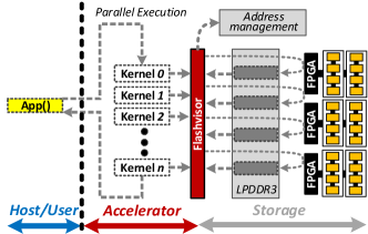
In this paper, we propose FlashAbacus, a data processing accelerator that self-governs heterogeneous computing and data storage by integrating many flash modules in lightweight multiprocessors to resemble a single low-power data processing unit. FlashAbacus employs tens of low-power functional units rather than hundreds and thousands of hardware threads that most manycore accelerators employ. Even though the computing capacity of the small number of functional units is not as high as that of the manycore accelerators, FlashAbacus can process data near flash with different types of applications or kernels that contain multiple functions or both. Such multi-kernel execution can maximize the resource utilization by dynamically scheduling multiple applications across all the internal processors. The kernel scheduler can also reorder the executions in an out of order manner by recognizing the code blocks that have no data dependency across different kernels of the target data-intensive application. Therefore, FlashAbacus offers high bandwidth with a relatively small number of processors, thereby maximizing energy efficiency.
A challenge in enabling such multi-kernel execution near flash is that the flash media integrated into the accelerator are not practically working memories; they operate in a manner similar to mass storage. That is, the cores of accelerator cannot execute any type of kernels through typical load and store instructions. Therefore, the accelerator needs to employ an OS, but the OS will make the accelerator bulkier and will worsen the performance characteristics. To address these challenges, we introduce Flashvisor that allows the cores of accelerator to access flash directly without any modification of the instruction set architecture or assistance of the host-side storage stack. Flashvisor virtualizes storage resources by mapping the data section of each kernel to physical flash memory. In addition, it protects flash from the simultaneous accesses of multi-kernel execution by employing a range lock, which requires a few memory resources. We also separate the flash management tasks from their address translations Kim et al. [2002]; Gupta et al. [2009]; Chung et al. [2009]; Park et al. [2008], and allocate a different processor to take over the flash management tasks. This separation makes the flash management mechanisms (e.g., garbage collection) invisible to the execution of multiple kernels.
We built a prototype FlashAbacus on a low-power multicore Instruments [2014] based PCIe platform that connects FPGA-based flash controllers with a 20 nm node process Xilinx [2015]. To evaluate the effectiveness of FlashAbacus prototype, we converted diverse computing applications Pouchet [2012] into our new execution framework. Our evaluation results show that FlashAbacus can offer 127% higher bandwidth and consume 78% less energy than a conventional hardware acceleration approach under data-intensive workloads.
2 Preliminaries
In this section, we analyze the overheads of moving data between an accelerator and storage, which are often observed in a conventional heterogeneous computing system. This section then explains the baseline architecture of our FlashAbacus.
2.1 Physical and Logical Data Paths
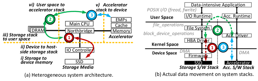
Hardware. Figure 1(a) shows the physical datapath with a CPU, a low-power accelerator, and an SSD in conventional heterogeneous computing. In cases where the accelerator needs to process a large amount of data, the CPU generates I/O requests and issues them to the underlying SSD through I/O controllers such as AHCI Jung [2016]; Intel [2010]. An SSD controller then transfers the data from flash to its internal DRAM, and the host controller again moves such data from the internal DRAM to the host-side DRAM through a storage interface Jung and Kandemir [2013]; Workgroup [2001]; Budruk et al. [2004] ( ). During this time, the data can be reconstructed and set in order as a form of objects that the accelerator can recognize ( ). Finally, the CPU transfers the data from the host-side DRAM to the internal DRAM of the accelerator through the PCIe interface again ( ). Note that, at this juncture, all kernel executions of the accelerator are still stalled because the input data are in being transferring and are not ready to be processed. Once the data are successfully downloaded, the embedded multicore processors (EMPs) of the accelerator can start processing the data, and the results will be delivered to the SSD in an inverse order of the input data loading procedure ( ). The movement of data across different physical interface boundaries imposes the restriction of long latency before the accelerator begins to actually process data and leads to a waste of energy, resulting from the creation of redundant memory copies. In addition, the physical datapath deteriorates the degree of parallelism for kernel executions. For example, a single application task has to be split into multiple kernels due to capacity limit of the internal DRAM of the accelerator, in turn requiring file-associated storage accesses and thereby serializing the execution.
Software. Another critical bottleneck for heterogeneous computing is the discrete software stacks, each of them exists for the accelerator and the SSD, respectively. As shown in Figure 1(b), the host needs to employ a device driver and a runtime library for the accelerator, while it requires a storage stack that consists of flash firmware, a host block adapter (HBA), a file system, and an I/O runtime to employ the underlying device as storage. The runtime libraries for the accelerator and the SSD offer different sets of interfaces, which allow a user application to service files or offload data processing, appropriately. In contrast, the accelerator driver and HBA driver are involved in transferring data between the device-side DRAM and host-side DRAM. Therefore, the user application first needs to request data to the underlying SSD through the I/O runtime library ( ), and then it must write data to the accelerator through the accelerator runtime library ( ). This activity causes multiple data copies within the host-side DRAM. Furthermore, when the file system and accelerator driver receive data from the application, all the data from user buffers must be copied to OS-kernel buffers, which again creates extra memory copies within the host-side DRAM ( ). This problem arises because OS-kernel modules cannot directly access the user memory space, as there is no guarantee that the current OS-kernel module is executing in the process that the I/O request was initiated. In addition to these unnecessary data copies (within the host-side DRAM), the discrete software stacks also increase data moving latency and consume energy because they enforce many user/privilege mode switches between their runtime libraries and OS-kernel drivers.
2.2 Baseline Architecture
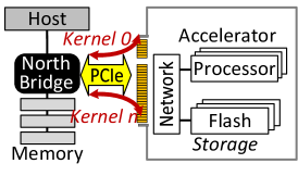
The datapath analysis in the previous section shows that the redundant memory copies across different devices are unnecessary if we can integrate the SSD directly into the accelerator, as shown in Figure 2a. The accelerator can also execute a series of tasks without an interruption if there is an enough memory space that can accommodate input data. Motivated by these observations, we built an FPGA-based flash backbone with a 20 nm processor node Xilinx [2015] and tightly integrated it into a commercially-available embedded SoC platform Instruments [2014], as shown in Figure 2b.
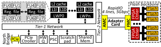
Multicore. To perform energy-efficient and low-power data processing near flash, our hardware platform employs multiple lightweight processors (LWPs) Instruments [2014], which are built on a VLIW architecture. The VLIW-based LWPs require neither out-of-order scheduling Lam [1988]; Fisher [1984] nor a runtime dependency check because these dynamics are shifted to compilers Ellis [1985]; Lee et al. [2000]. Each LWP has eight functional units (FUs) that consist of two multiplication FUs, four general purpose processing FUs, and two load/store FUs; thus, we can reduce the hardware complexity of the accelerator, while simultaneously satisfying the diverse demands of low-power data processing applications. In this design, LWPs are all connected over a high crossbar network, and they can communicate with each other over message queue interfaces that we implemented by collaborating with a hardware queue attached to the network TI [2015].
Memory system. Our hardware platform employs two different memory systems over the network that connects all LWPs: i) DDR3L and ii) scratchpad. While DDR3L consists of a large low-power DRAM Parameter Symbol [2012], the scratchpad is composed of eight high-speed SRAM banks Inc. [2007]. In our platform, DDR3L is used for mapping the data sections of each kernel to flash memory thereby hiding the long latency imposed by flash accesses. DDR3L is also capable of aggregating multiple I/O requests that head to the underlying storage modules, and feasible to buffer the majority of flash writes, which can take over the roles of the traditional SSD internal cache Wei et al. [2014]. In contrast, the scratchpad serves all administrative I/O requests by virtualizing the flash and the entries queued by the communication interfaces as fast as an L2 cache. Note that all LWPs share a single memory address space, but have their own private L1 and L2 caches.
| Components | Specification |
|
|
|
||||||
|---|---|---|---|---|---|---|---|---|---|---|
| LWP | 8 processors | 1GHz | 0.8W/core | 16GB/s | ||||||
| L1/L2 cache | 64KB/512KB | 500MHz | N/A | 16GB/s | ||||||
| Scratchpad | 4MB | 500MHz | N/A | 16GB/s | ||||||
| Memory | DDR3L, 1GB | 800MHz | 0.7W | 6.4GB/s | ||||||
| SSD | 16 dies, 32GB | 200MHz | 11W | 3.2GB/s | ||||||
| PCIe | v2.0, 2 lanes | 5GHz | 0.17W | 1GB/s | ||||||
| Tier-1 crossbar | 256 lanes | 500MHz | N/A | 16GB/s | ||||||
| Tier-2 crossbar | 128 lanes | 333MHz | N/A | 5.2GB/s |
Network organization. Our hardware platform uses a partial crossbar switch Sharma [1996] that separates a large network into two sets of crossbar configuration: i) a streaming crossbar (tier-1) and ii) multiple simplified-crossbars (tier-2). The tier-1 crossbar is designed towards high performance (thereby integrating multiple LWPs with memory modules), whereas throughputs of the tier-2 network are sufficient for the performances of Advanced Mezzanine Card (AMC) and PCIe interfaces exhibit Instruments . These two crossbars are connected over multiple network switches TI [2014d].
Flash backbone. Tier-2 network’s AMC is also connected to the FPGA Mezzanine Card (FMC) of the backend storage complex through four Serial RapidIO (SRIO) lanes (5Gbps/lane). In this work, the backend storage complex is referred to as flash backbone, which has four flash channels, each employing four flash packages over NV-DDR2 Semiconductor et al. [2006]. We introduce a FPGA-based flash controller for each channel, which converts the I/O requests from the processor network into the flash clock domain. To this end, our flash controller implements inbound and outbound “tag” queues, each of which is used for buffering the requests with minimum overheads. During the transition device domain, the controllers can handle flash transactions and transfer the corresponding data from the network to flash media through the SRIO lanes, which can minimize roles of flash firmware.
It should be noted that the backend storage is a self-existence module, separated from the computation complex via FMC in our baseline architecture. Since flash backbone is designed as a separable component, ones can simply replace worn-out flash packages with new flash (if it needs).
Prototype specification. Eight LWPs of our FlashAbacus operate with a 1GHz clock and each LWP has its own private 64KB L1 cache and 512KB L2 cache. The size of the 8-bank scratchpad is 4MB; DDR3L also consists of eight banks with a total size of 1GB. On the other hand, the flash backbone connects 16 triple-level cell (TLC) flash packages Micron [2014], each of which has two flash dies therein (32GB). Each of the four flash packages is connected to one of the four NV-DDR2 channels that work on ONFi 3.0 Semiconductor et al. [2006]. The 8KB page read and write latency are around 81 us and 2.6 ms, respectively. Lastly, the flash controllers are built on the 2 million system logic cells of Virtex Ultrascale FGPA Xilinx [2015]. The important characteristics of our prototype are presented in Table 1.
3 High-level View of Self-Governing
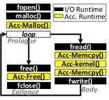
Figure 3a illustrates a kernel execution model for conventional hardware acceleration. In prologue, a data processing application needs to open a file and allocate memory resources for both an SSD and an accelerator. Its body iterates the code segments that read a part of file, transfer it to the accelerator, execute a kernel, get results from the accelerator, and write them back to the SSD. Once the execution of body loop is completed, the application concludes by releasing all the file and memory resources. This model operates well with traditional manycore-based high-performance accelerators that have thousands of hardware threads. However, in contrast to such traditional accelerators, the memory space of low-power accelerators is unfortunately limited and difficult to accommodate all data sets that an application requires to process. Thus, low-power accelerators demand more iterations of data transfers, which in turn can significantly increase I/O stack overheads. Furthermore, a small memory size of the low-power accelerators can enforce a single data-processing task split into multiple functions and kernels, which can only be executed by the target accelerator in a serial order.
3.1 Challenge Analysis
For better insights on the aforementioned challenges, we built a heterogeneous system that employs the low-power accelerator described in Section 2.2 and an NVMe SSD Intel [2015b] as external storage instead of our flash backbone.
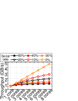
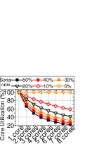
Utilization. Figures 3b and 3c show the results of our performance and utilization sensitivity studies in which the fraction of serial parts in kernel executions enforced by data transfers were varied. As the serial parts of a program increase, the throughput of data-processing significantly decreases (Figure 3b). For example, if there exists a kernel whose fraction of serialized executions is 30%, the performance degrades by 44%, on average, compared to the ideal case (e.g., 0%), thus the accelerator becomes non-scalable and the full benefits of heterogeneous computing are not achieved. Poor CPU utilization is the reason behind performance degradation (Figure 3c). For the previous example, processor utilization is less than 46%; even in cases where the serial parts take account for only 10% of the total kernel executions, the utilization can be less than at most 59%.
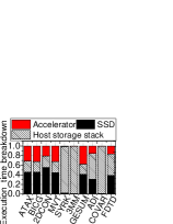
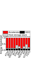
Storage accesses. We also evaluate the heterogeneous system by performing a collection of PolyBench Pouchet [2012] and decompose the execution time of each application into i) SSD latency to load/store input/output data, ii) CPU latency that host storage stack takes to transfer the data, and iii) accelerator latency to process the data111In this analysis, our accelerator latency includes the execution time that overlaps with the corresponding data transfer (DMA) time; the details of evaluation method and workload characteristics are described in Section 5 and Table 2, respectively.. Figure 3d shows that the data-intensive applications (e.g., ATAX, BICG, and MVT) consume 77% of the total execution time to transfer the data between the the accelerator and SSD. Figure 3e illustrates that the storage stack accesses, including file system operations and I/O services, consume 85% of the total energy in heterogeneous computing. Note that the data transfer overheads for computation-intensive applications (e.g., SYRK and 3MM) are not remarkable, but the corresponding energy consumed by the storage stack accounts for more than 77% of the total energy consumed by the system, on average. The detailed energy analysis of heterogeneous computing will be further discussed in Section 5.3.
To address the above two challenges, FlashAbacus governs the internal hardware resources without an assistance of host or OS. We introduce a multi-kernel execution model and storage monitor to fully utilize LWPs and virtualize flash backbone into processors’ memory address, respectively.
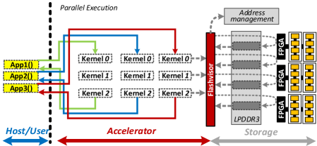
3.2 Multi-Kernel Execution
Hand-threaded parallelism (using pthread or message passing interface) can offer fine control than the parallel execution, but for such parallelism, it requires to accommodate OS thread management, which is infeasible to our low-power accelerator, have to be accommodated. In this work, we allow all the LWPs to execute different types of kernels in parallel, and each kernel can contain various operational functions. This in turn enables users to offload diverse user applications and perform different types of data processing in concert; this is referred to as multi-kernel execution. Figure 4a shows an example of the multi-kernel execution model. While a conventional kernel is a function that usually has a very simple iteration, our kernel can contain many functions and handle a deep depth of function calls. In this execution model, a host can also offload multiple kernels, which are associated with different applications in our accelerator (Figure 4b). While our multi-kernel execution is not as powerful as a thousand hardware thread executions that most manycore accelerators offer, it allows users to perform more flexible data processing near flash and opens up the opportunities to make data processing more energy efficient than in the conventional accelerators.
However, executing different kernels, each with many functions across multiple LWPs, can introduce other technical challenges such as load balancing and resource contention. To address these challenges, one can simply expose all internal LWP’s resources to the host so that users can finely control everything on their own. Unfortunately, this design choice can lead to a serious security problem, as an unauthorized user can access the internal resources and put them to an improper use. This approach may also introduce another type of data movement overheads as frequent communications are required to use diverse FlashAbacus resources from outside. Therefore, our accelerator internally governs all the kernels based on two different scheduling models: i) inter-kernel execution and ii) intra-kernel execution. In general, in inter-kernel executions, each LWP is dedicated to execute a specific kernel that performs data processing from the beginning to the end as a single instruction stream. In contrast, the intra-kernel execution splits a kernel into multiple code blocks and concurrently executes them across multiple LWPs based on the input data layout. The scheduling details will be explained in Section 4.
3.3 Fusing Flash into a Multicore System
The lack of file and runtime systems introduces several technical challenges to multi-kernel execution, including memory space management, I/O management, and resource protection. An easy-to-implement mechanism to address such issues is to read and write data on flash through a set of customized interfaces that the flash firmware may offer; this is the typically adopted mechanism in most active SSD approaches Jun et al. [2015]; Seshadri et al. [2014]. Unfortunately, this approach is inadequate for our low-power accelerator platform. Specifically, as the instruction streams (kernels) are independent of each other, they cannot dynamically be linked with flash firmware interfaces. Furthermore, for the active SSD approaches, all existing user applications must be modified by considering the flash interfaces, leading to an inflexible execution model.
Instead of allowing multiple kernels to access the flash firmware directly through a set of static firmware interfaces, we allocate an LWP to govern the memory space of the data section of each LWP by considering flash address spaces. This component, referred to as Flashvisor, manages the logical and physical address spaces of the flash backbone by grouping multiple physical pages across different dies and channels, and it maps the logical addresses to the memory of the data section. Note that all the mapping information is stored in the scratchpad, while the data associated with each kernel’s data sections are placed into DDR3L. In addition, Flashvisor isolates and protects the physical address space of flash backbone from the execution of multiple kernels. Whenever the kernel loaded to a specific LWP requires accessing its data section, it can inform Flashvisor about the logical address space where the target data exist by passing a message to Flashvisor. Flashvisor then checks a permission of such accesses and translates them to physical flash address. Lastly, Flashvisor issues the requests to the underling flash backbone, and the FPGA controllers bring the data to DDR3L. In this flash virtualization, most time-consuming tasks such as garbage collection or memory dump are periodically performed by a different LWP, which can address potential overheads brought by the flash management of Flashvisor (cf. Section 4.3). Note that, in contrast to a conventional virtual memory that requires paging over file system(s) and OS kernel memory module(s), our Flashvisor internally virtualizes the underlying flash backbone to offer a large-size of byte-addressable storage without any system software support. The implementation details of flash virtualization will be explained in Section 4.3.
4 Implementation Details
Kernel. The kernels are represented by an executable object TI [2014b], referred to as kernel description table. The description table, which is a variation of the executable and linkable format (ELF) Committee et al. [2001], includes an executable that contains several types of section information such as the kernel code (.text), data section (.ddr3_arr), heap (.heap), and stack (.stack). In our implementation, all the addresses of such sections point to the L2 cache of each LWP, except for the data section, which is managed by Flashvisor.
Offload. A user application can have one or more kernels, which can be offloaded from a host to a designated memory space of DDR3L through PCIe. The host can write the kernel description table associated with the target kernel to a PCIe base address register (BAR), which is mapped to DDR3L by the PCIe controller (cf. Figure 2b).
Execution. After the completion of the kernel download(s), the host issues a PCIe interrupt to the PCIe controller, and then the controller internally forwards the interrupt to Flashvisor. Flashvisor puts the target LWP (which will execute the kernel) in sleep mode through power/sleep controller (PSC) and stores DDR3L address of such a downloaded kernel to a special register, called boot address register of the target LWP. Flashvisor then writes an inter-process interrupt register of the target LWP, forcing this LWP to jump to the address written in the boot address register. Lastly, Flashvisor pulls the target LWP out of the sleep mode through PSC. Once this revocation process is completed, the target LWP begins to load and execute the specified kernel. Thus, Flashvisor can decide the order of kernel executions within an LWP across all LWPs.
4.1 Inter-kernel Execution
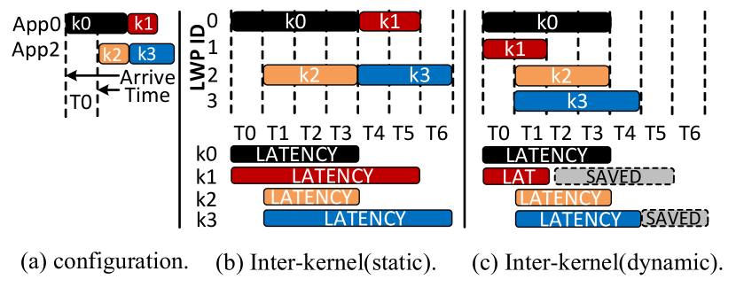
Static inter-kernel scheduling. The simplest method to execute heterogeneous kernels across multiple LWPs is to allocate each incoming kernel statically to a specific LWP based on the corresponding application number. Figures 5a shows that has two user applications, App0 and App2, each of which contains two kernels, respectively (e.g., k0/k1 for App0 and k2/k3 for App2). In this example, a static scheduler assigns all kernels associated with App0 and App2 to LWP0 and LWP2, respectively. Figure 5b shows the timing diagram of each LWP execution (top) and the corresponding latency of each kernel (bottom). Once a host issues all the kernels in App0 and App2, it does not require any further communication with the host until all computations are completed. Even though this static inter-kernel scheduling is easy to implement and manage in the multi-kernel execution model, such scheduling can unfortunately lead to a poor resource utilization due to the imbalance of kernel loads. For example, while LWP1 and LWP3 in idle, k1 and k3 should be suspended until the previously-issued k0 and k2 are completed.
Dynamic inter-kernel scheduling. To address the poor utilization issue behind static scheduling, Flashvisor can dynamically allocate and distribute different kernels among LWPs. If a new application has arrived, this scheduler assigns the corresponding kernels to any available LWPs in a round robin fashion. As shown in Figure 5c, k1 and k3 are allocated to LWP1 and LWP3, and they are executed in parallel with k0 and k2. Therefore, the latency of k1 and k3 are reduced as compared to the case of the static scheduler, by 2 and 3 time units, respectively. Since each LWP informs the completion of kernel execution to Flashvisor through the hardware queue (cf. Figure 2), Flashvisor can consecutively allocate next kernel to the target LWP. Therefore, this dynamic scheduler can fully utilize LWPs if it can secure sufficient kernel execution requests. However, there is still room to reduce the latency of each kernel while keeping all LWPs busy, if we can realize finer scheduling of kernels.
4.2 Intra-kernel Execution
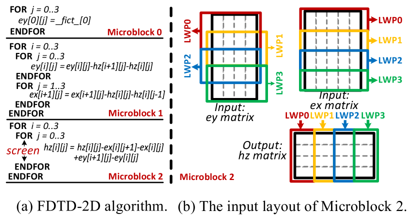
Microblocks and screens. In FlashAbacus, a kernel is composed of multiple groups of code segments, wherein the execution of each depends on their input/output data. We refer to such groups as microblocks. While the execution of different microblocks should be serialized, in several operations, different parts of the input vector can be processed in parallel. We call these operations (within a microblock) as screens, which can be executed across different LWPs. For example, Figure 6a shows the multiple microblocks observed in the kernel of (FDTD-2D) in Yee’s method Pouchet [2012]. The goal of this kernel is to obtain the final output matrix, hz, by processing the input vector, _fict_. Specifically, in microblock 0 (m0), this kernel first converts _fict_ (1D array) to ey (2D array). The kernel then prepares new ey and ex vectors by calculating ey/hz and ex/hz differentials in microblock 1 (m1). These temporary vectors are used for getting the final output hz at microblock 2 (m2). In m2, the execution codes per (inner loop) iteration generate one element of output vector, hz, at one time. Since there are no risks of write-after-write or read-after-write in m2, we can split the outer loop of m2 into four screens and allocate them across different LWPs for parallel executions. Figure 6b shows the input and output vector splitting and their mapping to the data sections of four LWPs to execute each screen.
In-order intra-kernel scheduling. This scheduler can simply assign various microblocks in a serial order, and simultaneously execute the numerous screens within a microblock by distributing them across multiple LWPs. Figure 7b shows an example of an in-order inter-kernel scheduler with the same scenario as that explained for Figure 5b. As shown in Figure 7a, k0’s m0 contains two screens ( and ), which are concurrently executed by different LWPs (LWP0 and LWP1). This scheduling can reduce 50% of k0’s latency compared to the static inter-kernel scheduler. Note that this scheduling method can shorten the individual latency for each kernel by incorporating parallelism at the screen-level, but it may increase the total execution time if the data size is not sufficiently large to partition as many screens as the number of available LWPs.
Out-of-order intra-kernel Scheduling. This scheduler can perform an out of order execution of many screens associated with different microblocks and different kernels. The main insight behind this method is that, the data dependency only exists among the microblocks within an application’s kernel. Thus, if there any available LWPs are observed, this scheduler borrows some screens from a different microblock, which exist across different kernel or application boundaries, and allocate the available LWPs to execute these screens. Similar to the dynamic inter-kernel scheduler, this method keeps all LWPs busy, which can maximize processor utilization, thereby achieving high throughput. Furthermore, the out-of-order execution of this scheduler can reduce the latency of each kernel. Figure 7c shows how the out-of-order scheduler can improve system performance, while maximizing processor utilization. As shown in the figure, this scheduler pulls the screen of k1’s microblock 0 (m0) from time unit (T1) and executes it at T0. This is because LWP2 and LWP3 are available even after executing all screens of k0’s microblock 0 (m0), and . With a same reason, the scheduler pulls the screen of k1’s microblock 2 (m2) from T3 and execute it at T1. Similarly, the screen of k2’s microblock 1 (m1) can be executed at T1 instead of T2. Thus, it can save 2, 4 and 4 time units for k0, k1 and k2, respectively (versus the static inter-kernel scheduler).
Note that, in this example, no screen is scheduled before the completion of all the screens along with a previous microblock. In FlashAbacus, this rule is managed by multi-app execution chain, which is a list that contains the data dependency information per application. Figure 8 shows the structure of multi-app execution chain; the root contains multiple pointers, each indicating a list of nodes. Each node maintains a series of screen information per microblock such as LWP ID and status of the execution. Note that the order of such nodes indicates the data-dependency relationships among the microblocks.
4.3 Flash Virtualization
The kernels on all LWPs can map the memory regions of DDR3L pointed by their own data sections to the designated flash backbone addresses. As shown in Figure 9, individual kernel can declare such flash-mapped space for each data section (e.g., input vector on DDR3L) by passing a queue message to Flashvisor. That is, the queue message contains a request type (e.g., read or write), a pointer to the data section, and a word-based address of flash backbone. Flashvisor then calculates the page group address by dividing the input flash backbone address, with the number of channel. If the request type is a read, Flashvisor refers its page mapping table with the page group number, and retrieves the corresponding page table entry, which contains the address of physical page group number. It then divides the translated group number by the total page number of each flash package, which indicates the package index within in a channel, and the remainder of the division can be the target physical page number. Flashvisor creates a memory request targeting the underlying flash backbone, and then all the FPGA controllers take over such requests. On the other hand, for a write request, Flashvisor allocates a new page group number by simply increasing the page group number used in a previous write. In cases where there is no more available page group number, Flashvisor generates a request to reclaim a physical block. Note that, since the time spent to lookup and update the mapping information should not be an overhead to virtualize the flash, the entire mapping table resides on scratchpad; to cover 32GB flash backbone with 64KB page group (4 channels * 2 planes per die * 8KB page), it only requires 2MB for address mapping. Considering other information that Flashvisor needs to maintain, a 4MB scratchpad is sufficient for covering the entire address space. Note that, since the page table entries associated with each block are also stored in the first two pages within the target physical block of flash backbone (practically used for metadata Zhang et al. [2015b]), the persistence of mapping information is guaranteed.
Protection and access control. While any of the multiple kernels in FlashAbacus can access the flash backbone, there is no direct data path between the FGPA controllers and other LWPs that process the data near flash. That is, all requests related to flash backbone should be taken and controlled by Flashvisor. An easy way by which Flashvisor can protect the flash backbone is to add permission information and the owner’s kernel number for each page to the page table entry. However, in contrast to the mapping table used for main memory virtualization, the entire mapping information of Flashvisor should be written in persistent storage and must be periodically updated considering flash I/O services such as garbage collection. Thus, adding such temporary information to the mapping table increases the complexity of our virtualization system, which can degrade overall system performance and shorten the life time of the underlying flash. Instead, Flashvisor uses a range lock for each flash-mapped data section. This lock mechanism blocks a request to map a kernel’s data section to flash if its flash address range overlaps with that of another by considering the request type. For example, the new data section will be mapped to flash for reads, and such flash address is being used for writes by another kernel, Flashvisor will block the request. Similarly, a request to map for writes will be blocked if the address of target flash is overlapped with another data section, which is being used for reads. Flashvisor implements this range lock by using red black tree structure Tarjan [1983]; the start page number of the data section mapping request is leveraged as a key, and each node is augmented with the last page number of the data section and mapping request type.
| Name | Description | MBLKs | Serial | Input | LD/ST | B/KI | Heterogeneous workloads | |||||||||||||
| MBLK | (MB) | ratio(%) | 1 | 2 | 3 | 4 | 5 | 6 | 7 | 8 | 9 | 10 | 11 | 12 | 13 | 14 | ||||
| ATAX | Matrix Transpose&Multip. | 2 | 1 | 640 | 45.61 | 68.86 | ⚫ | ⚫ | ⚫ | ⚫ | ||||||||||
| BICG | BiCG Sub Kernel | 2 | 1 | 640 | 46 | 72.3 | ⚫ | ⚫ | ⚫ | ⚫ | ||||||||||
| 2DCON | 2-Dimension Convolution | 1 | 0 | 640 | 23.96 | 35.59 | ⚫ | ⚫ | ⚫ | ⚫ | ⚫ | |||||||||
| MVT | Matrix Vector Prod.&Trans. | 1 | 0 | 640 | 45.1 | 72.05 | ⚫ | ⚫ | ⚫ | ⚫ | ⚫ | ⚫ | ⚫ | ⚫ | ⚫ | |||||
| ADI | Direction Implicit solver | 3 | 1 | 1920 | 23.96 | 35.59 | ⚫ | ⚫ | ⚫ | ⚫ | ⚫ | ⚫ | ⚫ | ⚫ | ⚫ | |||||
| FDTD | 2-D Finite Time Domain | 3 | 1 | 1920 | 27.27 | 38.52 | ⚫ | ⚫ | ⚫ | ⚫ | ⚫ | ⚫ | ⚫ | ⚫ | ||||||
| GESUM | Scalar, Vector&Multip. | 1 | 0 | 640 | 48.08 | 72.13 | ⚫ | ⚫ | ⚫ | ⚫ | ⚫ | ⚫ | ⚫ | ⚫ | ||||||
| SYRK | Symmetric rank-k op. | 1 | 0 | 1280 | 28.21 | 5.29 | ⚫ | ⚫ | ⚫ | ⚫ | ⚫ | |||||||||
| 3MM | 3-Matrix Multiplications | 3 | 1 | 2560 | 33.68 | 2.48 | ⚫ | ⚫ | ⚫ | ⚫ | ||||||||||
| COVAR | Covariance Computation | 3 | 1 | 640 | 34.33 | 2.86 | ⚫ | ⚫ | ⚫ | ⚫ | ⚫ | |||||||||
| GEMM | Matrix-Multiply | 1 | 0 | 192 | 30.77 | 5.29 | ⚫ | ⚫ | ⚫ | ⚫ | ⚫ | ⚫ | ⚫ | ⚫ | ||||||
| 2MM | 2-Matrix Multiplications | 2 | 1 | 2560 | 33.33 | 3.76 | ⚫ | ⚫ | ⚫ | ⚫ | ⚫ | ⚫ | ⚫ | |||||||
| SYR2K | Symmetric rank-k op. | 1 | 0 | 1280 | 30.19 | 1.85 | ⚫ | ⚫ | ⚫ | ⚫ | ||||||||||
| CORR | Correlation Computation | 4 | 1 | 640 | 33.04 | 2.79 | ⚫ | ⚫ | ⚫ | ⚫ | ||||||||||
Storage management. Flashvisor can perform address translation similar to a log-structured pure page mapping technique Kim et al. [2002], which is a key function of flash firmware Agrawal et al. [2008]. To manage the underlying flash appropriately, Flashvisor also performs metadata journaling Agrawal et al. [2008] and garbage collection (including wear-leveling) Bux and Iliadis [2010]; Chang [2007]; Shahidi et al. [2016]; Jung et al. [2012]. However, such activities can be strong design constraints for SSDs as they should be resilient in all types of power failures, including sudden power outages. Thus, such metadata journaling is performed in the foreground and garbage collection are invoked on demand Bux and Iliadis [2010]. In cases where an error is detected just before an uncorrectable error correction arises, Flashvisor excludes the corresponding block by remapping it with new one. In addition, all the operations of these activities are executed in the lockstep with address translation.
However, if these constraints can be relaxed to some extent, most overheads (that flash firmware bear brunt of) are removed from multi-kernel executions. Thus, we assign another LWP to perform this storage management rather than data processing. While Flashvisor is responsible for mainly address translation and multi-kernel execution scheduling, this LWP, referred to as Storengine, periodically dumps the scratchpad information to the underlying flash as described in the previous subsection. In addition, Storengine reclaims the physical block from the beginning of flash address space to the end in background. Most garbage collection and wear-leveling algorithms that are employed for flash firmware select victim blocks by considering the number of valid pages and the number of block erases. These approaches increase the accuracy of garbage collection and wear-leveling, since they require extra information to set such parameters and search of the entire address translation information to identify a victim block. Rather than wasting compute cycles to examine all the information in the page table, Storengine simply selects the target victim block from a used block pool in a round robin fashion and loads the corresponding page table entries from flash backbone. Storengine periodically migrates valid pages from the victim block to the new block, and return the victim to a free block in idle, which is a background process similar to preemtable firmware techniques Jung et al. [2014b, 2012]. Once the victim block is selected, the page mapping table associated with those two blocks is updated in both the scratchpad and flash. Note that all these activities of Storengine can be performed in parallel with the address translation of Flashvisor. Thus, locking the address ranges that Storengine generates for the snapshot of the scratchpad (journaling) or the block reclaim is necessary, but such activities overlapped with the kernel executions and address translations (are performed in the background).
5 Evaluation
Accelerators. We built five different heterogeneous computing options. “SIMD” employs a low-power accelerator that executes multiple data-processing instances using a single-instruction multiple-data (SIMD) model implemented in OpenMP Mitra et al. [2014], and SIMD performs I/Os through a discrete high-performance SSD (i.e., Intel NVMe 750 Intel [2015b]). On the other hand, “InterSt”, “InterDy”, “IntraIo”, and “IntraO3” employ the static inter-kernel, dynamic inter-kernel, in-order intra-kernel, and out-of-order intra-kernel schedulers of FlashAbacus, respectively. In these accelerated systems, we configure the host with Xeon CPU Intel [2015a] and 32GB DDR4 DRAM Standard [2012].
Benchmarks. We also implemented 14 real benchmarks that stem from Polybench Pouchet [2012] on all our accelerated systems222In this implementation, we leverage a set of TI code generation tools TI [2014a, 2011, c] to develop and compile the kernels of our FlashAbacus. Note that the memory protection and access control are regulated by the TI’s tools, which may be limited for other types of acceleration hardware.. To evaluate the impact of serial instructions in the multi-core platform, we rephrase partial instructions of tested benchmarks to follow a manner of serial execution. The configuration details and descriptions for each application are explained in Table 2. In this table, we explain how many microblocks exist in an application (denoted by MBLKs). Serial MBLK refers to the number of microblocks that have no screens; these microblocks are to be executed in serial. The table also provides several workload analyses, such as the input data size of an instance (Input), ratio of load/store instructions to the total number of instructions (LD/ST ratio), and computation complexity in terms of data volumes to process per thousand instructions (B/KI). To evaluate the benefits of different accelerated systems, we also created 14 heterogeneous workloads by mixing six applications. All these configurations are presented at the right side of the table, where the symbol indicates the correspondent applications, which are included for such heterogeneous workloads.
Profile methods. To analyze the execution time breakdown of our accelerated systems, we instrument timestamp annotations in both host-side and accelerator-side application source codes by using a set of real-time clock registers and interfaces. The annotations for each scheduling point, data transfer time, and execution period enable us to capture the details of CPU active cycles and accelerator execution cycles at runtime. On the other hand, we use a blktrace analysis Axboe et al. [2010] to measure device-level SSD performance by removing performance interference potentially brought by any modules in storage stack. We leverage Intel power gadget tool to collect the host CPU energy and host DRAM energy Kim et al. [2014]. Lastly, we estimate the energy consumption of FlashAbacus hardware platform based on TI internal platform power calculator, and use our in-house power analyzer to monitor the dynamic power of SSD Jung [2016]; Zhang et al. [2014].
5.1 Data Processing Throughput
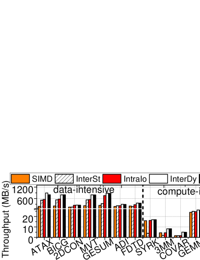
Figure 10 demonstrates the overall throughput of all hardware accelerators that we implemented by executing both homogeneous workloads and heterogeneous workloads. Generally speaking, the proposed FlashAbacus approach (i.e., IntraO3) outperforms the conventional accelerator approach SIMD by 127%, on average, across all workloads tested.
Homogeneous workloads. Figure 10a shows the overall throughput evaluated from homogeneous workloads. In this evaluation, we generate 6 instances from each kernel. Based on the computation complexity (B/KI), we categorize all workloads into two groups: i) data-intensive and ii) computing-intensive. As shown in the figure, all our FlashAbacus approaches outperform SIMD for data-intensive workloads by 144%, on average. This is because, although all the accelerators have equal same computing powers, SIMD cannot process data before the data are brought by the host system. However, InterSt has poorer performance, compared to InterDy and IntraO3, by 53% and 52%, respectively. The reason is that InterSt is limited to spreading homogeneous workloads across multiple workers, due to its static scheduler configuration. Unlike InterSt, IntraIo enjoys the benefits of parallelism, by partitioning kernels into many screens and assigning them to multiple LWPs. However, IntraIo cannot fully utilize multiple LWPs if there is a microblock that has no code segments and that cannot be concurrently executed (i.e., serial MBLK). Compared to IntraIo, IntraO3 successfully overcomes the limits of serial MBLK by borrowing multiple screens from different microblocks, thereby improving the performance by 62%, on average. For homogeneous workloads, InterDy achieves the best performance, because all the kernels are equally assigned to a single LWP and are simultaneously completed. While IntraO3 can dynamically schedule microblocks to LWPs for a better load balance, IPC overheads (between Flashvisor and workers) and scheduling latency of out-of-order execution degrade IntraO3’s performance by 2%, on average, compared to InterDy.
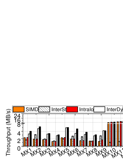
Heterogeneous workloads. Figure 10b shows the overall system bandwidths of different accelerated systems under heterogeneous workloads. For each execution, we generate 24 instances, four from a single kernel. SIMD exhibits 3.5 MB/s system bandwidth across all heterogeneous workloads, on average, which is 98% worse than that of data-intensive workloads. This is because, heterogeneous workloads contain computing-intensive kernels, which involve much longer latency in processing data than storage accesses. Although the overheads imposed by data movement are not significant in computing-intensive workloads, the limited scheduling flexibility of SIMD degrades performance by 42% and 50%, compared to InterDy and IntraO3, respectively. In contrast to the poor performance observed in homogeneous workloads, InterSt outperforms IntraIo by 34% in workloads MX2,3,4,6,7,9 and 13. This is because SIMD can statically map 6 different kernels to 6 workers. However, since different kernels have various data processing speeds, unbalanced loads across workers degrade performance by 51%, compared to IntraIo, for workloads MX1,5,8,10,11 and 12. Unlike InterSt, InterDy monitors the status of workers and dynamically assigns a kernel to a free worker to achieve better load balance. Consequently, InterDy exhibits 177% better performance than InterSt. Compared to the best performance reported by the previous homogeneous workload evaluations, performance degradation of InterDy in these workloads is caused by a stagger kernel, which exhibits much longer latency than other kernels. In contrast, IntraO3 shortens the latency of the stagger kernel by executing it across multiple LWPs in parallel. As a result, IntraO3 outperforms InterDy by 15%.
5.2 Execution Time Analysis
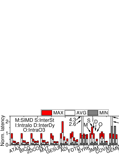
Homogeneous workloads. Figure 11a analyzes latency of the accelerated systems (with homogeneous workloads). For data-intensive workloads (i.e., ATAX, BICG, 2DCONV, and MVT), average latency, maximum latency, and minimum latency of SIMD are 39%, 87%, and 113% longer than those of FlashAbacus approaches, respectively. This is because, SIMD consumes extra latency to transfer data through different I/O interfaces and redundantly copy I/Os across different software stacks. InterSt and InterDy exhibit similar minimum latency. However, InterDy has 57% and 68% shorter average latency and maximum latency, respectively, compared to InterSt. This is because, InterSt can dynamically schedule multiple kernels across different workers in parallel. The minimum latency of inter-kernel schedulers (InterSt and InterDy) is 61% longer than that of intra-kernel schedulers (IntraIo and IntraO3), because intra-kernel schedulers can shorten single kernel execution by leveraging multiple cores to execute microblocks in parallel.
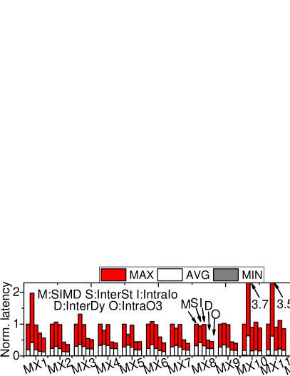
Heterogeneous workloads. Figure 11b shows the same latency analysis, but with heterogeneous workloads. All heterogeneous workloads have more computing parts than the homogeneous ones, data movement overheads are hidden behind their computation somewhat. Consequently, SIMD exhibits kernel execution latency similar to that of IntraIo. Meanwhile, InterSt exhibits a shorter maximum latency for workloads MX4,5,8 and 14, compared to IntraIo. This is because, these workloads contain multiple serial microblocks that stagger kernel execution. Further InterSt has the longest average latency among all tested approaches due to inflexible scheduling strategy. Since IntraO3 can split kernels into multiple screens and achieve a higher level of parallelism with a finer-granule scheduling, it performs better than InterDy in terms of the average and maximum latency by 10% and 19%, respectively.
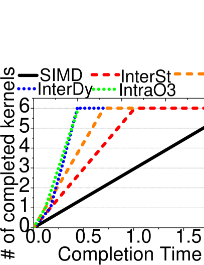
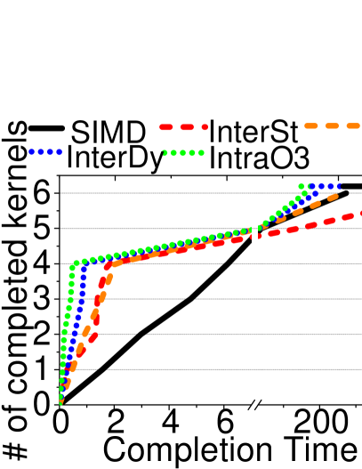
CDF analysis. Figures 12a and 12b depict the execution details of workload ATAX and MX1, each representing homogeneous and heterogeneous workloads, respectively. As shown in Figure 12a, InterDy takes more time to complete the first kernel compared to IntraIo and IntraO3, because InterDy only allocates single LWP to process the first kernel. For all the six kernels, InterO3 also completes the operation earlier than or about the same time as InterDy. More benefits can be achieved by heterogeneous execution. As shown in Figure 12b, for the first four data-intensive kernels, SIMD exhibits much longer latency compared to FlashAbacus, due to the system overheads. While SIMD outperforms InterSt for the last two computation-intensive kernels, IntraO3 outperforms SIMD by 42%, on average.
5.3 Energy Evaluation
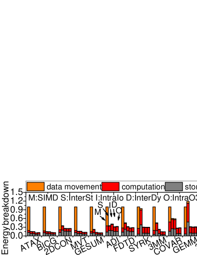
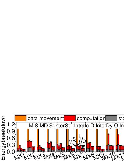
In Figure 13, the energy of all five tested accelerated systems is decomposed into the data movement, computation and storage access parts. Overall, IntraO3 consumes average energy less than SIMD by 78.4% for all the workloads that we tested. Specifically, all FlashAbacus approaches exhibit better energy efficiency than SIMD for data-intensive workloads (cf. Figure 13a). This is because, the host requires periodic transfer of data between the SSD and accelerator, consuming 71% of the total energy of SIMD. Note that, InterSt consumes 28% more energy than SIMD for computing-intensive workloads, GEMM, 2MM, and SYR2K. Even though InterSt cannot fully activate all workers due to its inflexibility, it must keep Flashvisor and Storengine always busy for their entire execution, leading to inefficient energy consumption behavior. However, IntraIo, InterDy, and IntraO3 reduce the overall energy consumption by 47%, 22%, and 2%, respectively, compared to InterSt. This is because IntraO3 can exploit the massive parallelism (among all workers), saving energy, wasted by the idle workers (observed by InterSt).
5.4 Processor Utilizations
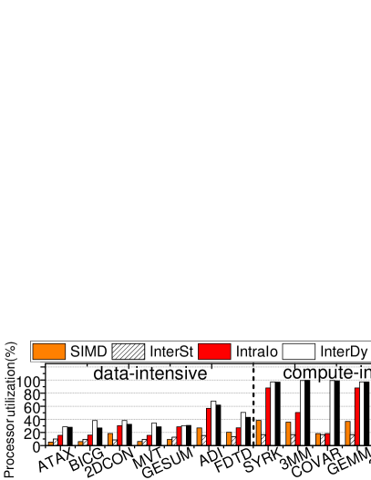
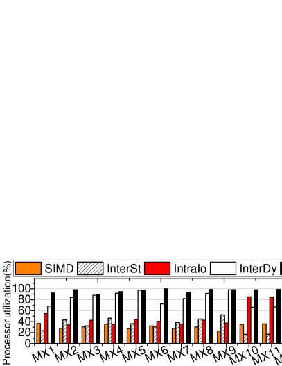
Figures 14a and 14b show an analysis of LWP utilizations obtained by executing homogeneous and heterogeneous workloads. In this evaluation, LWP utilization is calculated by dividing the LWP’s actual execution time (average) by the latency to execute entire application(s) in each workload. For data-intensive ones, most of LWP executions are stalled due to the long latency of storage accesses, which make SIMD’s LWP utilizations lower than InterO3 by 23%, on average. On the other hand, InterDy keeps all processors busy by 98% of the total execution time, which leads the highest LWP utilization among all accelerated systems we tested. IntraO3 schedules microblocks in out-of-order manner and only a small piece of code segment is executed each time, which makes its LWP utilization slightly worse than InterDy ones (less than 1%) for the execution of homogeneous kernels. In contrast, for heterogeneous kernel executions, IntraO3 achieves processor utilization over 94%, on average, 15% better than that of InterDy. Since LWP utilization is strongly connected to the degree of parallelism and computing bandwidth, we can conclude that IntraO3 outperforms all the accelerated systems.
5.5 Dynamics in Data Processing and Power
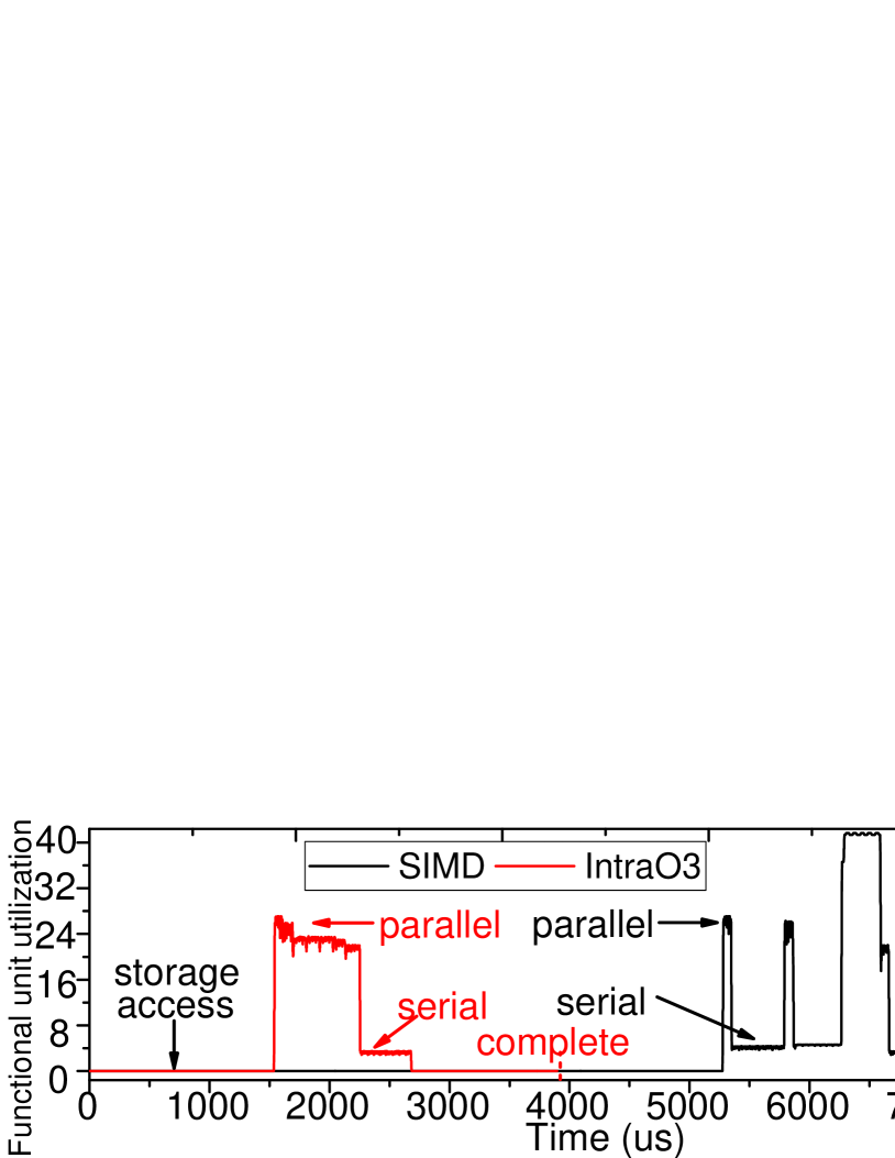
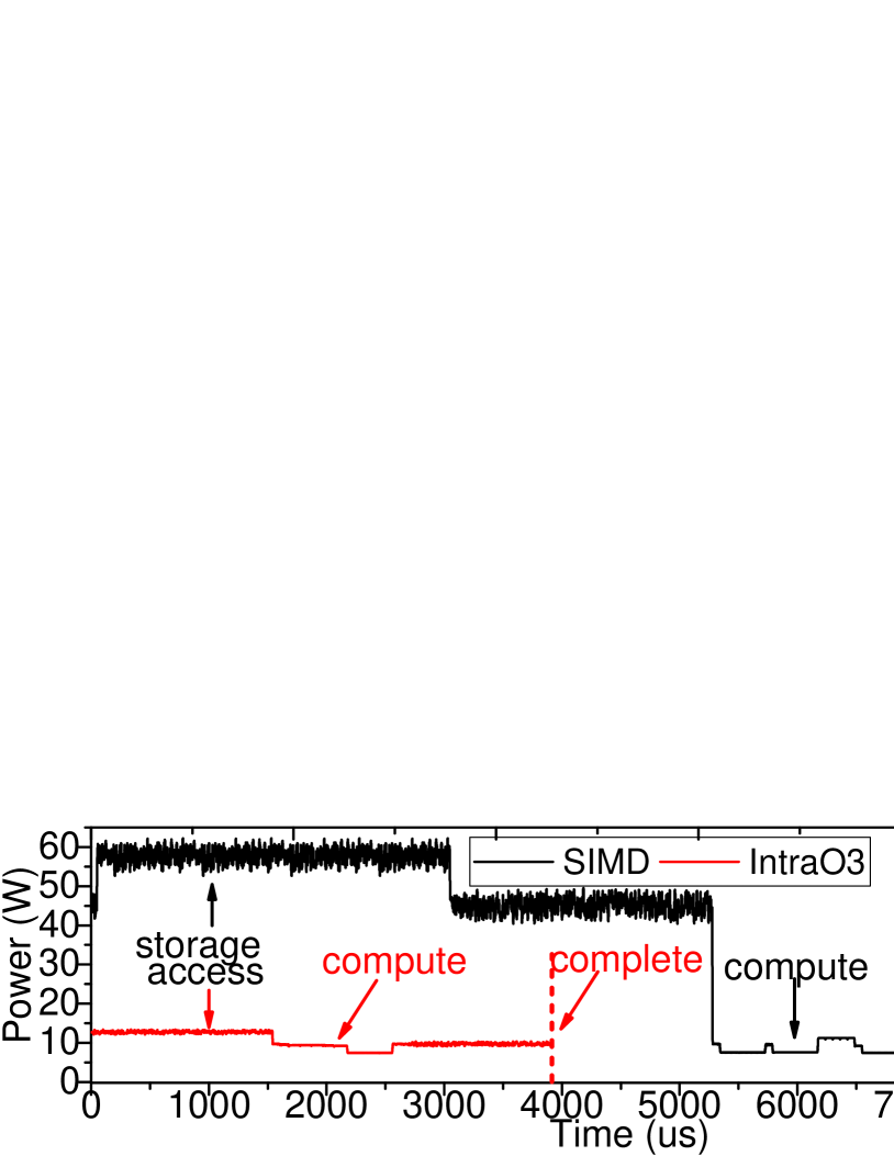
Figures 15a and 15b illustrate the time series analysis results for utilizing functional units and power usage of workers, respectively. In this evaluation, we compare the results of IntraO3 with those for SIMD to understand in detail the runtime behavior of the proposed system. As shown in Figure 15a, IntraO3 achieves shorter execution latency and better function unit utilization than SIMD. This is because, IntraO3 can perform parallel execution of multiple serial microblocks in multiple cores, which increases the function unit utilization. In addition, due to the shorter storage access, IntraO3 can complete the execution 3600 us earlier than SIMD. On the other hand, IntraO3 exhibits much lower power consumption than SIMD during storage access (Figure 15b). This is because SIMD requires the assistance of host CPU and main memory in transferring data between the SSD and accelerator, which in turn consumes 3.3x more power than IntraO3. Interestingly, the pure computation power of IntraO3 is 21% higher than SIMD, because IntraO3 enables more active function units to perform data processing, thus taking more dynamic power.
5.6 Extended Evaluation on Real-world Applications
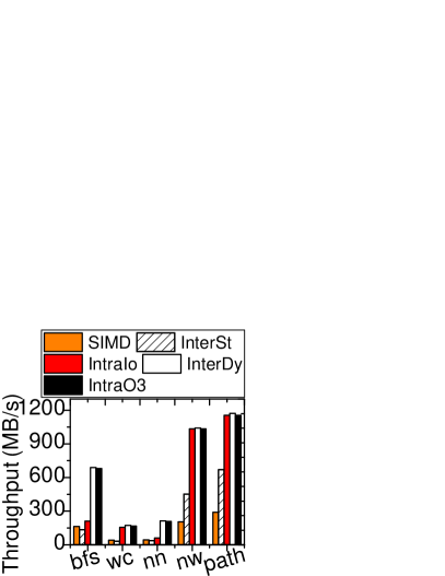
Application selection. In this section, we select five representative data-intensive workloads coming from graph benchmarks Che et al. [2009] and bigdata benchmarks He et al. [2008] in order to better understand system behaviors with real applications: i) K-nearest neighbor (nn), ii) graph traversal (bfs), iii) DNA sequence searching (nw), iv) grid traversal (path) and v) mapreduce wordcount (wc)).
Performance. Figure 16a illustrates data processing throughput of our FlashAbacus by executing the graph/bigdata benchmarks. One can observe from this figure that the average throughput of FlashAbacus approaches (i.e., IntraIo, InterDy and IntraO3) outperform SIMD by 2.1x, 3.4x and 3.4x, respectively, for all data-intensive workloads that we tested. Even though SIMD can fully utilize all LWPs, and it is expected to bring an excellent throughput for the workloads that have no serialized faction of microblocks (i.e., nw and path), SIMD unfortunately exhibits poor performance than other FlashAbacus approaches. This performance degradation is observed because LWPs are frequently stalled and bear brunt of comparably long latency imposed by moving the target data between its accelerator and external SSD over multiple interface and software intervention boundaries. Similarly, while SIMD’s computation capability is powerful much more than InterSt’s one, which requires to execute multiple kernels in a serial order, InterSt’s average throughput is 120% and 131% better than SIMD’s performance for nw and path, respectively.
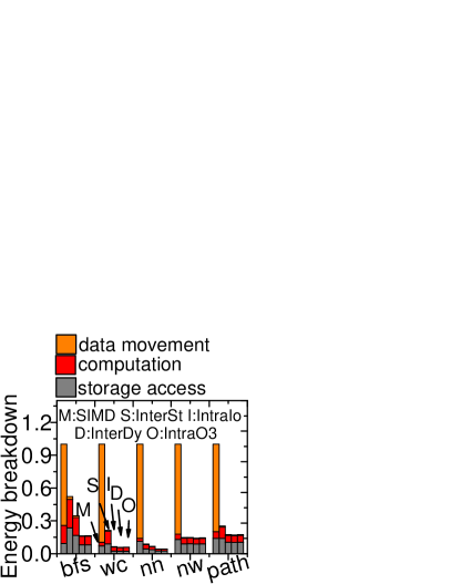
Energy. We also decompose the total energy of the system, which is used for each data-intensive application, into i) data movement, ii) computation, and iii) storage access; each item represents the host energy consumed for transferring data between the accelerator and SSD, the actual energy used by accelerator to compute, and the energy involved in serving I/O requests, respectively. The results of this energy breakdown analysis is illustrated by Figure 16b. One can observe from this figure that InterSt, IntraI0, InterDy and IntraO3 can save the total average energy for processing all data by 74%, 83%, 88% and 88%, compared to SIMD, respectively. One of the reasons behind of this energy saving is that the cost of data transfers account for 79% of the total energy cost in SIMD, while FlashAbacus eliminates the energy, wasted in moving the data between the accelerator and SSD. We observe that the computation efficiency of InterDy and IntraO3 also is better than that SIMD for even the workloads that have serial microblocks (i.e., bfs and nn). This is because OpenMP that SIMD use should serialize the executions of serial microblocks, whereas Flashvisor of the proposed FlashAbacus coordinates such serial microblocks from different kernels and schedule them across different LWPs in parallel.
6 Discussion and Related Work
Platform selection. The multicore-based PCIe platform we select Instruments [2014] integrates a terabit-bandwidth crossbar network for multi-core communication, which potentially make the platform a scale-out accelerator system (by adding up more LWPs into the network). In addition, considering a low power budget (5W 20W), the platform we implemented FlashAbacuse has been considered as one of the most energy efficient (and fast) accelerator in processing a massive set of data Hegde et al. [2016]. Specifically, it provides 358 Gops/s with 25.6 Gops/s/W power efficiency, while other low-power multiprocessors such as a many-core system Parallella , a mobile GPU Nvidia [2015]; Otterness et al. [2017], a FPGA-based accelerator Xilinx are available to offer 10.5, 256 and 11.5 Gops/s with 2.6, 25.6 and 0.3 Gops/s/W power efficiency, respectively.
Limits of this study. While the backend storage complex of FlashAbacus is designed as a self-existent module, we believe that it is difficult to replace with conventional off-the-shelf SSD solutions. This is because our solution builds flash firmware solution from scratch, which is especially customized for flash virtualization. We select a high-end FPGA for the flash transaction controls as research purpose, but the actual performance of flash management we believe cannot be equal to or better than microcoded ASIC-based flash controller due to the limit of low frequency of FPGA. Another limit behind this work is that we are unfortunately not able to implement FlashAbacus in different accelerators such as GPGPU due to access limits for such hardware platforms and a lack of supports for code generations. However, we believe that the proposed self-governing design (e.g., flash integration and multi-kernel execution) can be applied to any type of hardware accelerators if vendor supports or open their IPs, which will outperform many accelerators that require employing an external storage.
Hardware/software integration. To address the overheads of data movements, several hardware approaches tried to directly reduce long datapath that sit between different computing devices. For example, Shainer et al. [2011]; Ahn et al. [2015]; Foley [2014] forward the target data directly among different PCIe devices without a CPU intervention. System-on-chip approachs that tightly integrate CPUs and accelerators over shared memory Damaraju et al. [2012]; Wolf et al. [2008], which can reduce the data transfers between. However, these hardware approaches cannot completely address the overheads imposed by discrete software stacks. Since SSDs are block devices, which can be shared by many other user applications, all the SSD accesses should be controlled by the storage stack appropriately. Otherwise, the system cannot guarantee the durability of storage, and simultaneous data access without an access control of storage stack can make data inconsistent, in turn leading to a system crash. In contrast, a few previous studies explored reducing the overheads of moving data between an accelerator and a storage by optimizing the software stack of the two devices Zhang et al. [2015a]; Tseng et al. [2016]; Silberstein et al. [2013]. However, these studies cannot remove all limitations imposed by different physical interface boundaries, and unfortunately, their solutions highly depends on the target system’s software and software environment.
In-storage processing. Prior studies Cho et al. [2013]; Tiwari et al. [2013]; Gu et al. [2016]; Acharya et al. [1998]; Keeton et al. [1998] proposed to eliminate the data movement overheads by leveraging the existing controller to execute a kernel in storage. However, these in-storage process approaches are limited to a single core execution and their computation flexibility is strictly limited by the APIs built at the design stage. Jun et al. [2015] integrates SSD controller and data processing engine within a single FPGA, which supports parallel data access and host task processing. While this FPGA-based approach is well optimized for a specific application, porting the current host programs to RTL design can bring huge burdens to programmers and still inflexible to adopt many different types of data-intensive applications at runtime. FlashAbacus governs the storage within an accelerator and directly executes multiple general applications across multiple light-weight processors without any limit imposed by the storage firmware or APIs.
Open-channel or cross-layer optimization. Many proposals also paid attention on cross-layer optimizations or open-channel SSD approaches that migrates firmware from the device to kernel or partitions some functionalities of flash controller and implement it into OS Bernhard III et al. [2014]; Jung and Kandemir [2012]; Ouyang et al. [2014]; Lee et al. [2016]; Huang et al. [2015]; Jung et al. [2014a]. While all these studies focused on managing the underlying flash memory and SSD efficiently, they have a lack of considerations on putting data processing and storage together in an hardware platform. In addition, since these proposals cannot be applied into an single hardware accelerator, which has no storage stack, but requires byte-addressability to access the underlying storage complex.
7 Conclusion
In this work, we combined flash with lightweight multi-core accelerators to carry out energy-efficient data processing. Our proposed accelerator can offload various kernels in an executable form and process parallel data. Our accelerator can improve performance by 127%, while requiring 78% less energy, compared to a multi-core accelerator that needs external storage accesses for data-processing.
8 Acknowledgement
This research is mainly supported by NRF 2016R1C1B2015312 and MemRay grant (2015-11- 1731). This work is also supported in part by, DOE DEAC02-05CH 11231, IITP-2017-2017-0-01015, and NRF2015M3C4A7065645. The authors thank Gilles Muller for shepherding this paper. We also thank MemRay Corporation and Texas Instruments for their research sample donation and technical support. Myoungsoo jung is the corresponding author.
References
- pas [2016] Nvidia gp100 architecture whitepaper. White paper, 2016.
- Acharya et al. [1998] A. Acharya, M. Uysal, and J. Saltz. Active disks: Programming model, algorithms and evaluation. In ACM SIGOPS Operating Systems Review, volume 32, pages 81–91. ACM, 1998.
- Agrawal et al. [2008] N. Agrawal, V. Prabhakaran, T. Wobber, J. D. Davis, M. S. Manasse, and R. Panigrahy. Design tradeoffs for ssd performance. In USENIX Annual Technical Conference, pages 57–70, 2008.
- Ahn et al. [2015] J. Ahn, D. Kwon, Y. Kim, M. Ajdari, J. Lee, and J. Kim. Dcs: a fast and scalable device-centric server architecture. In Proceedings of the 48th International Symposium on Microarchitecture, pages 559–571. ACM, 2015.
- Arora et al. [2012] M. Arora, S. Nath, S. Mazumdar, S. B. Baden, and D. M. Tullsen. Redefining the role of the cpu in the era of cpu-gpu integration. Micro, IEEE, 32(6):4–16, 2012.
- Axboe et al. [2010] J. Axboe, A. D. Brunelle, and N. Scott. Blktrace, 2010.
- Bernhard III et al. [2014] L. F. Bernhard III, L. D. Desai, and M. H. Jacobson. Cooperative memory management, Nov. 18 2014. US Patent 8,892,827.
- Borriello and Want [2000] G. Borriello and R. Want. Embedded computation meets the world wide web. Communications of the ACM, 43(5):59–66, 2000.
- Budruk et al. [2004] R. Budruk, D. Anderson, and T. Shanley. PCI express system architecture. Addison-Wesley Professional, 2004.
- Bux and Iliadis [2010] W. Bux and I. Iliadis. Performance of greedy garbage collection in flash-based solid-state drives. Performance Evaluation, 67(11):1172–1186, 2010.
- Chang [2007] L.-P. Chang. On efficient wear leveling for large-scale flash-memory storage systems. In Proceedings of the 2007 ACM symposium on Applied computing, pages 1126–1130. ACM, 2007.
- Che et al. [2009] S. Che, M. Boyer, J. Meng, D. Tarjan, J. W. Sheaffer, S.-H. Lee, and K. Skadron. Rodinia: A benchmark suite for heterogeneous computing. In Workload Characterization, 2009. IISWC 2009. IEEE International Symposium on, pages 44–54. Ieee, 2009.
- Cho et al. [2013] S. Cho, C. Park, H. Oh, S. Kim, Y. Yi, and G. R. Ganger. Active disk meets flash: A case for intelligent ssds. In Proceedings of the 27th international ACM conference on International conference on supercomputing, pages 91–102. ACM, 2013.
- Chrysos [2014] G. Chrysos. Intel® xeon phi™ coprocessor-the architecture. Intel Whitepaper, 176, 2014.
- Chung et al. [2009] T.-S. Chung, D.-J. Park, S. Park, D.-H. Lee, S.-W. Lee, and H.-J. Song. A survey of flash translation layer. Journal of Systems Architecture, 55(5-6):332–343, 2009.
- Committee et al. [2001] T. I. S. Committee et al. Executable and linkable format (elf). Specification, Unix System Laboratories, 2001.
- Damaraju et al. [2012] S. Damaraju, V. George, S. Jahagirdar, T. Khondker, R. Milstrey, S. Sarkar, S. Siers, I. Stolero, and A. Subbiah. A 22nm ia multi-cpu and gpu system-on-chip. In Solid-State Circuits Conference Digest of Technical Papers (ISSCC), 2012 IEEE International, pages 56–57. IEEE, 2012.
- Ellis [1985] J. R. Ellis. Bulldog: A compiler for vliw architectures. Technical report, Yale Univ., New Haven, CT (USA), 1985.
- Fisher [1984] J. A. Fisher. The vliw machine: a multiprocessor for compiling scientific code. Computer, 17(7):45–53, 1984.
- Foley [2014] D. Foley. Nvlink, pascal and stacked memory: Feeding the appetite for big data. Nvidia. com, 2014.
- Govindaraju et al. [2008] N. K. Govindaraju, B. Lloyd, Y. Dotsenko, B. Smith, and J. Manferdelli. High performance discrete fourier transforms on graphics processors. In Proceedings of the 2008 ACM/IEEE conference on Supercomputing, page 2. IEEE Press, 2008.
- Gu et al. [2016] B. Gu, A. S. Yoon, D.-H. Bae, I. Jo, J. Lee, J. Yoon, J.-U. Kang, M. Kwon, C. Yoon, S. Cho, et al. Biscuit: A framework for near-data processing of big data workloads. In Computer Architecture (ISCA), 2016 ACM/IEEE 43rd Annual International Symposium on, pages 153–165. IEEE, 2016.
- Gupta et al. [2009] A. Gupta, Y. Kim, and B. Urgaonkar. DFTL: a flash translation layer employing demand-based selective caching of page-level address mappings, volume 44. ACM, 2009.
- He et al. [2008] B. He, W. Fang, Q. Luo, N. K. Govindaraju, and T. Wang. Mars: a mapreduce framework on graphics processors. In Proceedings of the 17th international conference on Parallel architectures and compilation techniques, pages 260–269. ACM, 2008.
- Hegde et al. [2016] G. Hegde, N. Ramasamy, N. Kapre, et al. Caffepresso: an optimized library for deep learning on embedded accelerator-based platforms. In Proceedings of the International Conference on Compilers, Architectures and Synthesis for Embedded Systems, page 14. ACM, 2016.
- Huang et al. [2015] J. Huang, A. Badam, M. K. Qureshi, and K. Schwan. Unified address translation for memory-mapped ssds with flashmap. In Computer Architecture (ISCA), 2015 ACM/IEEE 42nd Annual International Symposium on, pages 580–591. IEEE, 2015.
- Inc. [2007] A. M. Inc. 512k x 16 bit super low power cmos sram datasheet. URL:http://www.alliancememory.com/pdf/AS6C8016.pdf, 2007.
- [28] T. Instruments. Throughput performance guide for keystone ii devices.
- Instruments [2014] T. Instruments. Multicore fixed and floating-point digital signal processor (tms320c6678). URL:http://www.ti.com/lit/ds/symlink/tms320c6678.pdf, 2014.
- Intel [2010] Intel. Advanced host controller interface specification. URL:http://www.intel.com/content/www/us/en/io/serial-ata/ahci.html, 2010.
- Intel [2015a] Intel. Intel xeon processor e5 2620 v3. URL:http://ark.intel.com/products/83352/Intel-Xeon-Processor-E5-2620-v3-15M-Cache-2-40-GHz, 2015a.
- Intel [2015b] Intel. Intel ssd 750 series. URL:http://www.intel.com/content/www/us/en/solid-state-drives/solid-state-drives-750-series.html, 2015b.
- Jun et al. [2015] S.-W. Jun, M. Liu, S. Lee, J. Hicks, J. Ankcorn, M. King, S. Xu, et al. Bluedbm: an appliance for big data analytics. In Computer Architecture (ISCA), 2015 ACM/IEEE 42nd Annual International Symposium on, pages 1–13. IEEE, 2015.
- Jung [2016] M. Jung. Exploring design challenges in getting solid state drives closer to cpu. IEEE Transactions on Computers, 65(4):1103–1115, 2016.
- Jung [2017] M. Jung. Nearzero: An integration of phase change memory with multi-core coprocessor. IEEE Computer Architecture Letters, 16(2):136–140, 2017.
- Jung and Kandemir [2012] M. Jung and M. Kandemir. Middleware-firmware cooperation for high-speed solid state drives. In Proceedings of the Posters and Demo Track, page 5. ACM, 2012.
- Jung and Kandemir [2013] M. Jung and M. Kandemir. Challenges in getting flash drives closer to cpu. Future, 2(4.00):8–00, 2013.
- Jung et al. [2012] M. Jung, R. Prabhakar, and M. T. Kandemir. Taking garbage collection overheads off the critical path in ssds. In ACM/IFIP/USENIX International Conference on Distributed Systems Platforms and Open Distributed Processing, pages 164–186. Springer, 2012.
- Jung et al. [2014a] M. Jung, W. Choi, J. Shalf, and M. T. Kandemir. Triple-a: a non-ssd based autonomic all-flash array for high performance storage systems. In ACM SIGARCH Computer Architecture News, volume 42, pages 441–454. ACM, 2014a.
- Jung et al. [2014b] M. Jung, W. Choi, S. Srikantaiah, J. Yoo, and M. T. Kandemir. Hios: a host interface i/o scheduler for solid state disks. In ACM SIGARCH Computer Architecture News, volume 42, pages 289–300. IEEE Press, 2014b.
- Keeton et al. [1998] K. Keeton, D. A. Patterson, and J. M. Hellerstein. A case for intelligent disks (idisks). ACM SIGMOD Record, 27(3):42–52, 1998.
- Kim et al. [2002] J. Kim, J. M. Kim, S. H. Noh, S. L. Min, and Y. Cho. A space-efficient flash translation layer for compactflash systems. IEEE Transactions on Consumer Electronics, 48(2):366–375, 2002.
- Kim et al. [2014] S.-W. Kim, J. J.-S. Lee, V. Dugar, and J. De Vega. Intel® power gadget. Intel Corporation, 7, 2014.
- Lam [1988] M. Lam. Software pipelining: An effective scheduling technique for vliw machines. In ACM Sigplan Notices, volume 23, pages 318–328. ACM, 1988.
- Lee et al. [2000] C. Lee, J. K. Lee, T. Hwang, and S.-C. Tsai. Compiler optimization on instruction scheduling for low power. In Proceedings of the 13th international symposium on System synthesis, pages 55–60. IEEE Computer Society, 2000.
- Lee et al. [2016] S. Lee, M. Liu, S. W. Jun, S. Xu, J. Kim, and A. Arvind. Application-managed flash. In FAST, pages 339–353, 2016.
- Manavski et al. [2007] S. Manavski et al. Cuda compatible gpu as an efficient hardware accelerator for aes cryptography. In Signal Processing and Communications, 2007. ICSPC 2007. IEEE International Conference on, pages 65–68. IEEE, 2007.
- Micron [2014] Micron. Mt29f64g08. URL:http://goo.gl/GXV5Qq, 2014.
- Mitra et al. [2014] G. Mitra, E. Stotzer, A. Jayaraj, and A. P. Rendell. Implementation and optimization of the openmp accelerator model for the ti keystone ii architecture. In International Workshop on OpenMP, pages 202–214. Springer, 2014.
- NVIDIA [2016] NVIDIA. Pascal GPU Architecture http://www.nvidia.com/object/pascal-architecture-whitepaper.html. 2016.
- Nvidia [2015] J. T. Nvidia. Nvidia jetson tx1 system-on-module, 2015.
- Otterness et al. [2017] N. Otterness, M. Yang, S. Rust, E. Park, J. H. Anderson, F. D. Smith, A. Berg, and S. Wang. An evaluation of the nvidia tx1 for supporting real-time computer-vision workloads. In Real-Time and Embedded Technology and Applications Symposium (RTAS), 2017 IEEE, pages 353–364. IEEE, 2017.
- Ouyang et al. [2014] J. Ouyang, S. Lin, S. Jiang, Z. Hou, Y. Wang, and Y. Wang. Sdf: Software-defined flash for web-scale internet storage systems. In ACM SIGPLAN Notices, volume 49, pages 471–484. ACM, 2014.
- [54] Parallella. Epiphany-iii 16-core microprocessor. http://www.adapteva.com/epiphanyiii/.
- Parameter Symbol [2012] D. Parameter Symbol. Ddr3l-1333 ddr3/ddr3l-1600 units notes min. Max. Min. Max, 2012.
- Park et al. [2008] C. Park, W. Cheon, J. Kang, K. Roh, W. Cho, and J.-S. Kim. A reconfigurable ftl (flash translation layer) architecture for nand flash-based applications. ACM Transactions on Embedded Computing Systems (TECS), 7(4):38, 2008.
- Pouchet [2012] L.-N. Pouchet. Polybench: The polyhedral benchmark suite. URL: http://www. cs. ucla. edu/~ pouchet/software/polybench/[cited July,], 2012.
- Semiconductor et al. [2006] H. Semiconductor et al. Open nand flash interface specification. Technical report, Technical Report Revision 1.0, ONFI, www. onfi. org, 28th December, 2006.
- Seshadri et al. [2014] S. Seshadri, M. Gahagan, S. Bhaskaran, T. Bunker, A. De, Y. Jin, Y. Liu, and S. Swanson. Willow: A user-programmable ssd. In Proceedings of the 11th USENIX conference on Operating Systems Design and Implementation, pages 67–80. USENIX Association, 2014.
- Shahidi et al. [2016] N. Shahidi, M. Arjomand, M. Jung, M. T. Kandemir, C. R. Das, and A. Sivasubramaniam. Exploring the potentials of parallel garbage collection in ssds for enterprise storage systems. In Proceedings of the International Conference for High Performance Computing, Networking, Storage and Analysis, page 48. IEEE Press, 2016.
- Shainer et al. [2011] G. Shainer, A. Ayoub, P. Lui, T. Liu, M. Kagan, C. R. Trott, G. Scantlen, and P. S. Crozier. The development of mellanox/nvidia gpudirect over infiniband—a new model for gpu to gpu communications. Computer Science-Research and Development, 26(3-4):267–273, 2011.
- Sharma [1996] V. Sharma. Crossbar switch for multi-processor, multi-memory system for resolving port and bank contention through the use of aligners, routers, and serializers, Sept. 24 1996. US Patent 5,559,970.
- Silberstein et al. [2013] M. Silberstein, B. Ford, I. Keidar, and E. Witchel. Gpufs: integrating a file system with gpus. In ACM SIGPLAN Notices, volume 48, pages 485–498. ACM, 2013.
- Standard [2012] J. Standard. Ddr4 sdram. JEDEC Solid State Technology Association, JESD79-4, 151, 2012.
- Tarjan [1983] R. E. Tarjan. Updating a balanced search tree in o (1) rotations. Information Processing Letters, 16(5):253–257, 1983.
- TI [2011] TI. Multicore software development kit. URL:https://training.ti.com/multicore-software-development-kit-mcsdk-keystone-devices, 2011.
- TI [2014a] TI. Ti code generation tools. URL:http://processors.wiki.ti.com/index.php/Category:Compiler, 2014a.
- TI [2014b] TI. Common object file format. URL:http://www.ti.com/lit/an/spraao8/spraao8.pdf, 2014b.
- TI [2014c] TI. Multicore application deployment (mad) utilities. URL:http://processors.wiki.ti.com/index.php/MAD-Utils-User-Guide, 2014c.
- TI [2014d] TI. Ti keystone architecture. URL:http://www.ti.com/lit/ml/sprt548/sprt548.pdf, 2014d.
- TI [2015] TI. Keystone architecture multicore navigator. URL:http://www.ti.com/lit/ug/sprugr9h/sprugr9h.pdf, 2015.
- Tiwari et al. [2013] D. Tiwari, S. Boboila, S. S. Vazhkudai, Y. Kim, X. Ma, P. Desnoyers, and Y. Solihin. Active flash: towards energy-efficient, in-situ data analytics on extreme-scale machines. In FAST, pages 119–132, 2013.
- Tseng et al. [2016] H.-W. Tseng, Q. Zhao, Y. Zhou, M. Gahagan, and S. Swanson. Morpheus: creating application objects efficiently for heterogeneous computing. ISCA, 2016.
- Wei et al. [2014] Q. Wei, C. Chen, and J. Yang. Cbm: A cooperative buffer management for ssd. In Mass Storage Systems and Technologies (MSST), 2014 30th Symposium on, pages 1–12. IEEE, 2014.
- Wolf et al. [2008] W. Wolf, A. A. Jerraya, and G. Martin. Multiprocessor system-on-chip (mpsoc) technology. IEEE Transactions on Computer-Aided Design of Integrated Circuits and Systems, 27(10):1701–1713, 2008.
- Workgroup [2001] S. A. Workgroup. Sata: High speed serialized at attachment. X Y D D, 2001.
- [77] Xilinx. Vc707 evaluation board for the virtex-7 fpga. https://www.xilinx.com/support/documentation/boards_and_kits/vc707/ug885_VC707_Eval_Bd.pdf.
- Xilinx [2015] Xilinx. Virtex ultrascale. URL:https://www.xilinx.com/products/silicon-devices/fpga/virtex-ultrascale.html, 2015.
- Zhang et al. [2014] J. Zhang, M. Shihab, and M. Jung. Power, energy and thermal considerations in ssd-based i/o acceleration. In Proceedings of the 6th USENIX conference on Hot Topics in Storage and File Systems, pages 15–15. USENIX Association, 2014.
- Zhang et al. [2015a] J. Zhang, D. Donofrio, J. Shalf, M. T. Kandemir, and M. Jung. Nvmmu: A non-volatile memory management unit for heterogeneous gpu-ssd architectures. In 2015 International Conference on Parallel Architecture and Compilation (PACT), pages 13–24. IEEE, 2015a.
- Zhang et al. [2015b] J. Zhang, G. Park, M. M. Shihab, D. Donofrio, J. Shalf, and M. Jung. Opennvm: An open-sourced fpga-based nvm controller for low level memory characterization. In Computer Design (ICCD), 2015 33rd IEEE International Conference on, pages 666–673. IEEE, 2015b.