High Figure of Merit Magneto Optics from Interfacial Skyrmions on Topological Insulators
Abstract
In the Kerr rotation geometry, magneto optic memory devices typically suffer from low figure-of-merit (FOM) and long write times. We show that skyrmions formed at the interface of a thin-film multiferroic and a topological insulator can give rise to high FOM magneto optic Kerr effects (MOKEs). Huge differential MOKE can arise in parts of the phase diagram. Resonance like features in the MOKE spectra arising from the induced low energy TI bandgap, the multiferroic-film thickness, and the high energy Drude like behavior are resolved and explained. The Fermi level dependence of the MOKE signatures is distinct for the different magnetic textures. This has broad implications for magnetic texture characterization, electro-optic modulators and isolators and high density magnetic optic memory.
March 15, 2024
Magneto-optic (MO) phenomenon such as Kerr and Faraday rotations, Voigt effect, magneto-plasma reflections and cyclotron resonances arise from broken time reversal symmetry. Some MO effects also arise from the electronic structure’s topology, and hence are used to study quantum hall effectsKukushkin and Timofeev (1996), Kerr rotations in topological insulators (TIs)Tse and MacDonald (2010, 2011), magneto-electric optical effectsArima (2008); Atmatzakis et al. (2018), magneto-chiral effectsSessoli et al. (2015), and skyrmions and their Hall effectsVomir et al. (2016); Woo et al. (2018); Jiang et al. (2017).
The magneto optic Kerr effect (MOKE) in the polar configuration is particularly interesting due to its application in optical reading–out of magnetically stored informationHansen (1990); Suzuki et al. (1992); MANSURIPUR (2000) A MOKE device can be characterized by its figure-of-merit (FOM)Mansuripur (1986); Challener (1995); Taussig et al. (2008), which usually depends on the Kerr rotation angle and the reflectivity. Typically, during the MO memory write process, a focussed laser heats the magnetic material to its Curie temperature, which allows the local magnetic polarization to be flipped. However, the thermally–assisted write processes can be relatively slow. For readout, the Kerr rotation is barely one degree for most MO recording materials Lairson and Clemens (1993); Van Engen et al. (1983); Egashira and Yamada (1974); Reim and Weller (1988), which can result in higher readout error rates. The Kerr rotation can be enhanced by the use of cavity like resonance conditions, but this usually lowers the reflectivity and makes the memory write process difficult. The required magnetic fields and effective cyclotron frequencies for generating large Kerr rotations in a semi-infinite medium can be unreasonably largeDe and Puri (2002a, 2003). However, skyrmions can give rise to very high emergent fields. The emergent magnetic fields from a periodic lattice of skyrmions (SkX) can reach up to Tesla, which is two orders of magnitude larger than what can be generated in laboratories.
Skyrmions are topological particle-like configurations of continuous vector fields and are regarded as analogs of magnetic monopoles as each skyrmion is associated with a quantized magnetic fluxGross et al. (2018); Li et al. (2014). Their non-trivial topology is a result of competing Dzyaloshinkii-Moriya-(DM), Heisenberg- and Zeeman-interactions Jiang et al. (2017); Tolley et al. (2018); Luo et al. (2018). In addition, Skyrmions represent a new type of magnetic orderRößler et al. (2006); Mühlbauer et al. (2009), and they have been observed in B20 compounds such as MnSiTonomura et al. (2012); Yu et al. (2013), FeCoSiYu et al. (2010), FeGeHuang and Chien (2012) and in Cu2OSeO3 which is a multiferroicSeki et al. (2012). Skyrmions have been proposed for use in novel high density electrically controllable racetrack memoriesZhu et al. (2018); Yu et al. (2016).
The use of magneticMochizuki (2012) and electric fieldsMochizuki and Watanabe (2015a) has been proposed to switch between the topologically nontrivial skyrmion spin texture and the topologically trivial ferromagnetic spin texture. Experimentally it is possible create and erase individual skyrmions using spin polarized currentsRomming et al. (2013a). Also magnetic skyrmions can be electrically created on a thin-film of a chiral-lattice magnetic insulator within a few nanoseconds by applying an electric field which couples to the noncollinear skyrmion spinsNakatani et al. (2016); White et al. (2012); Koshibae et al. (2015); Schott et al. (2017); Okamura et al. (2016); Mochizuki and Watanabe (2015b); Romming et al. (2013b). In Cu2OSeO3, the noncollinear skyrmion spin structure in the host material behaves like a multiferroic due to spin–orbit coupling. This enables skyrmion manipulaton via electric fields instead of electric currents Everschor et al. (2011); Zang et al. (2011) or heat pulses Koshibae and Nagaosa (2014). More recently it has been shown that one can reversibly switch between topologically inequivalent ferromagnetic phases and skyrmion phases using electric fields Hsu et al. (2016). A topological charge analysis of skyrmion dynamics, energetics, creation, and stability was recently described Yin et al. (2016).
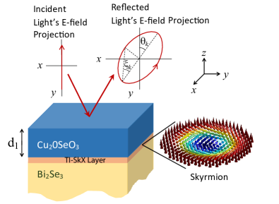
Skyrmions combined with other topological materials can lead to emergent functionalities. In this paper, we show that a skyrmion lattice at the interface of a thin-film B20 compound (such as Cu2OSeO3) and a semiinfinite TI (e.g. Bi2Se3) gives rise to a high FOM-MOKE (see Fig. 1). The large MOKE can be exploited for characterization of the spin texture, or application in a magneto–optic memory device.
Skyrmions can form on a TI’s surfaceYasuda et al. (2016) and can become chargedHurst et al. (2015). The B20–TI heterostructure provides electric field switching of the skyrmion spin texture and a large MOKE from the skyrmion phase. The large differential MOKE leads to fast and high fidelity magneto–optical bit readout. Electric field switching provides fast, low–power writing. The emergent properties of the B20–TI heterostructure provide the physical mechanisms for facile reading and writing of information bits in a topological magneto-optic memory.
For simplicity we consider a device geometry where a seminfinite TI is capped by a thin Cu2OSeO3 layer as shown in Fig. 1. We consider interfaces with a ferromagnetic (FM) texture along with Néel- and Bloch type skyrmions. This simple geometry allows us to best highlight the main MOKE spectral features manifesting from different physical effects. These are: the low energy topological MOKE, thin-film induced enhancement of MOKE and MOKE occurring at the high energy plasma frequency.
Model and Method: We begin by constructing a model where the surface of the TI is coupled to the background spin texture of a SkX. A low energy effective model describing the surface state of Bi2Se3 is used where the surface state consists of a single Dirac cone at the point Lu et al. (2010).
We consider the low energy effective HamiltonianXia et al. (2009) describing the decoupled top and bottom surface states of a TI To avoid the well known Fermion doubling problem on discrete tight-binding lattice, we have added a term to the Hamiltonian of TISusskind (1977); Hong et al. (2012)
| (1) |
where the Fermi velocity , is a material constant. This momentum space Hamiltonian can be transformed into the following real space tight binding Hamiltonian coupled to the Skx spin texture on a rectangular lattice
| (2) |
where is the localized spin of the skyrmion on site which couples to the TI through the Hund’s rule coupling constant . Here is the nearest neighbor hopping along the and directions, is the spin of the itinerant electron, and is the on site potential. Periodic boundary conditions are imposed along both the and directed edges of a square unit cell consisting of lattice sites. We define two dimensionless parameters and . Here, , , . For our numerical simulations we choose the discretization length , , ms and meV. Yasuda et al. (2016) The interplay between and dictates the anomalous Hall conductivity of the TI surface in this model.
The magnetization of a single skyrmion can be described by
| (3) |
where , and . Lado and Fernández-Rossier (2015) and where the helicity of the skyrmion is defined by the phase . Nagaosa and Tokura (2013) In this paper, we consider both Néel type and Bloch type skyrmions . The skyrmion is centered in the unit cell, and the magnetization is evaluated at each lattice site to obtain in Eq. (2).
The -component of acts on the electron like position dependent Dirac mass, while the in-plane components can give rise to an emergent gauge field. The total magnetic flux enclosed in a unit skyrmion cell is one flux quantum, , independent of the skyrmion radius, . Hamamoto et al. (2015) The effective magnetic field is . Kanazawa et al. (2015)
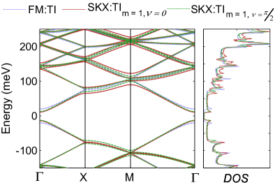
Electronic Structure: The numerically calculated band structure and the corresponding density of states (DOS) are shown in Fig. 2 for the magnetic textures proximity coupled to the TI. This includes the ferromagnetic case (FM:TI), the Néel type skyrmion (), and the Bloch type skyrmion () proximity coupled to the TI’s surface state. The energy gap at resulting from proximity coupling to the Néel and Bloch type skyrmions is less than the gap resulting from proximity coupling to the FM state. This can be understood from the fact that the skyrmion creates a hole in the background FM texture that reduces the total component of the magnetic moment. The presence of the skyrmions also breaks the degeneracy in other higher energy regions of the spectrum.
Dielectric Tensor Components: Observables such as magneto optic effects and quantum Hall type phenomenon manifest themselves through the dielectric tensor components which depend on the electronic structure and topological properties. In the case of normal optical incidence for an SkX on a TI, the magnetization is along , which is perpendicular to the surface and parallel to the direction of light propagation, similar to the polar Kerr effect. The and directions preserve in-plane symmetry. The complex dielectric tensor has diagonal terms and the off-diagonal terms which are topology dependent.
The matrix elements of the optical conductivity tensor can be obtained from the band structure calculations using the Kubo formula Thouless et al. (1982); Kohmoto (1985) as follows:
| (4) |
where is the velocity operator. Here , is a broadening parameter and , is the energy difference of an optical transition between an unoccupied band, and an occupied band, . , where is the Fermi filling factor.
Since we are using an effective Hamiltonian to obtain , we compensate for the missing higher band contributions in Eq. (4) by adding a ) term while relating the optical dielectric tensor to the conductivity tensor.
| (5) |
Here is adjusted so that the relative zero frequency dielectric constant matches the known experimental value. is the vacuum permittivity. For Bi2Se3, is given by Lorentz oscillator fits to experiment Eddrief et al. (2016), which in the low energy regime ( meV) is essentially a constant. In the effective surface model, the bulk band contributions to the momentum matrix elements in are not included. However, this does not change the qualitative behavior of the effects shown in this paper, since the calculated s are qualitatively similar to experimentEddrief et al. (2016). Therefore we argue that all the higher energy MOKE features disccused in this paper would still be seen in experiments, but at higher optical frequencies.
The dielectric function consists of Berry connection type terms, , which behave like a fictitious momentum space gauge potential or an equivalent magnetic field . The MOKE can therefore be viewed as an optical manifestation of the Berry curvature via the term. This is similar to charge transport, where the response is proportional to the Chern number Rößler et al. (2006); Jackson et al. (1985); Münzer et al. (2010); Yu et al. (2012), which is the integral of Berry curvature over the first Brillouin zone, . There are differences between MOKE and quantum Hall effect type topological manifestations due to conduction valance transitions and the frequency dependence in optics. depends on the topological charge across a gap. Usually is much smaller than the diagonal . In our case the three different magnetic textures result in the same Chern number across the fundamental gap of the proximity induced magnetic TI surface state, so that does not vary much when the Fermi energy is set to 0.
Magneto-Optics: The complex in-plane index of refraction is where, the signs represents right(left) circularly polarized (RCP(LCP)) light propagation. The complex MOKE effect is expressed as: where the Kerr rotation and ellipticity are, respectively
| (6) | |||||
| (7) |
Since the eigen-modes here are LCP and RCP, the Kerr rotation angle can be expressed as the phase difference between these two modes. The complex phase can be obtained from the Fresnel reflection coefficients .
The MOKE arising because of the thin-film structure can be significantly altered by internal reflection at various interfaces of the layers. A characteristic matrix method can be used to characterize the MOKE spectra of a multilayer structure at normal incidence, assuming that the materials are homogeneous and isotropic. The transfer matrices are in the LCP/RCP eigenmode basis, which for parallel layers is:
| (12) |
The Fresnel reflection and transmission coefficients at normal incidence for each interface are respectively given by: and The phase factor is given by , where is the thickness of the layer and is the optical wavelength. The complex reflection coefficient from the resultant characteristic transfer matrix is: where . The observed reflective intensity is .
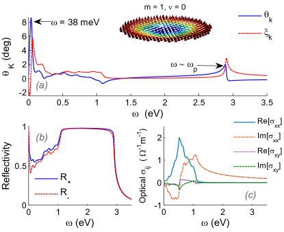
Discussion: We first consider only an ideal single interface for our initial analysis. The MOKE spectra and reflectivity and the optical dielectric function are shown for a Néel type skyrmion () on a TI in Fig. 3 for illustration. The corresponding spectra for FM:TI and Bloch type skyrmion () on a TI look very similar.
Two distinct resonance like features can be seen for the Kerr rotation and the elipticity. From the approximationArgyres (1955): , it is easy to see that MOKE resonances spectrally occurs whenever De and Puri (2002a). In Fig. 3, one MOKE resonance is in the low energy regime and occurs at 38 meV. This is close to the size of the fundamental gap that the magnetic texture (Néel type skyrmion in this case) induces in the TI. We will explore this regime, where the quantization effects occurs, in more detail later in this paper.
The high energy MOKE resonance features occur in the energy regime where free electron like behavior dominates. Hence this can be qualitatively understood from the semiclassical Drude model: , where is the plasma frequency and is the cyclotron frequency.
If Argyres (1955), an additional approximation can be made for the Kerr rotation, . From this most commonly used expression for calculating MOKE, it can be seen that MOKE resonances should occur when . This is also where goes to zero and the MOKE resonance occurs near Feil and Haas (1987); De and Puri (2002b); Abe and Suwa (2004). Note that similarly, magneto-plasmons in graphene give large magneto optic effectsFerreira et al. (2012); Tymchenko et al. (2013). Using the Drude model, one can derive a simple expression for the spectral occurrence of this MOKE resonanceDe and Puri (2002a)
| (13) |
In an attempt to explain the high energy spectral features using the Drude model, we extract the effective and effective using the optical sum rules:
| (14) | |||||
| (15) |
These values can be substituted into Eq. (13) to obtain , which is listed in Table 1 along with other parameters. The analytically obtained is in excellent agreement with – which is the frequency at which the high energy MOKE resonance occurs. In this high energy regime, the magnitude of as shown in Table 1. Overall if then the Kerr rotation resonance is at . Whereas if then a large MOKE resonance edge split occurs at frequencies determined by De and Puri (2002a). Note that these calculations are for a single interface (i.e. assuming both the Cu2OSeO3 and Bi2Se3 layers are semi-infinite).
| Spin Texture | (eV) | (eV) | (eV) | (eV) | |
|---|---|---|---|---|---|
| FM | 2.175 | 2.822 | 0.014 | 2.894 | 2.878 |
| 2.032 | 2.816 | 0.013 | 2.888 | 2.872 | |
| 2.029 | 2.816 | 0.013 | 2.889 | 2.872 |
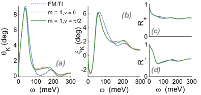
We next consider the MOKE features around 38 meV. The MOKE spectra is shown in Fig. 4 in the energy regime below 300 meV. The maximum Kerr rotation is about , which occurs when are the furthest apart as this increases . The Kerr rotation is sufficiently large for magneto-optic recording applications. In this case, there is not a clear distinguishing feature between the interface with the FM and the interface with the two different skyrmion spin textures. For these calculations, the Fermi Energy, . The MOKE spectral features in this energy regime are primarily dominated by the gap in the TI surface state, which is induced by the magnetic textures. The Chern number in the gap is the same for all three magnetic textures, and hence there is no clear distinction in the MOKE features for .
MOKE can also be enhanced by the resonance like effects that arise from adjusting the film thickness of different materials. In order to understand the effects of this for our system, we consider a thin-film structure as shown in Fig. 1 where a Cu2OSeO3 film of thickness sits on a semi-infinite Bi2Se3 layer. The dispersion relation for Cu2OSeO3 was obtained using experimentally fitted Lorentz oscillatorsMiller et al. (2010). As is typical with multiferroics, there are several low energy phonon modes present in the Cu2OSeO3 dielectric function which are also reproduced by the modelMiller et al. (2010). We assume that the SkX system exists in a 1 nm thin layer at the interface of the Cu2OSeO3 thin film and seminfinite Bi2Se3 layer. The SkX:TI effects manifest themselves via . The refractive index of air is used for the semi-infinite media above the Cu2OSeO3 layer as shown in Fig. 1.
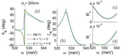
A comparison of the magneto optic Kerr rotation, ellipticity, LCP and RCP reflectivity spectra are shown in Fig. 5 for a Néel type skyrmion, the Bloch type skyrmion, and the FM:TI for a Cu2OSeO3 layer with film thickness . At this particular film thickness, , which causes a huge Kerr rotation resonance of as the phase difference between LCP and RCP is maximized. Also for a given film thicknesses for the Cu2OSeO3 layer, the MOKE spectra can be notably different between the different SkX textures and the FM state. In this example the maximum Kerr rotation arising from the FM:TI is deg and occurs at a different optical frequency.
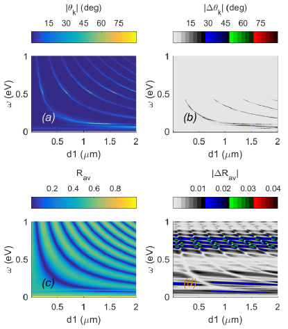
In order to achieve low error magneto-optic readouts, the different states should be maximally discernable. We therefore examine the phase diagram, as a function of and , for the differential MOKE effects,
| (16) | |||||
| (17) |
where is the average reflectivity. We take to avoid Kerr rotations greater than deg.
The phase diagram for both the Kerr rotation and the average reflectivity is shown in Fig. 6 (a) and (c) for the Néel type skyrmion. Both Néel- and Bloch-type skyrmions have identical phase diagrams where and vary periodically with and . There are several periodic parts of this phase diagram that are insensitive to errors in film-thickness or spectral tuning. By tuning a large Kerr rotation can be obtained for any frequency meV. The reflectivity would, however, be low in this case when is maximized. The differential and effects are shown in Fig. 6 (b) and (d), respectively. Generally is low. The FM:TI and SkX:TI have slightly different periodicity. Therefore the differential Kerr rotation can reach up to depending on . The phase diagram also suggests that either the Néel- or Bloch-type skyrmions could be used for such a magneto-optic recording device.
Typically, large Kerr rotations are accompanied by low reflectivities which reduces the effectiveness of a MO device. The overall useful MO signal can be quantified by the figure of merit (FOM)Mansuripur (1986); Challener (1995); Taussig et al. (2008) for the Kerr rotation configuration, defined here as,
| (18) |
This can be used to characterize MO memory and other MO devices such as modulators and isolators.
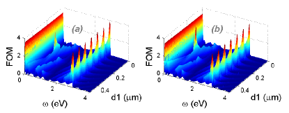
For our device, the FOM is shown in Fig. 7 as a function of and . At eV, the FOM peaks, arising from the free electron behavior, periodically as a function of . The FOM resonance at eV, and m is due to the features shown in Fig. 5. Even though , the FOM is not the highest due to low . The FOM peak here is higher for the Néel SkX:TI than it is for the FM:TI. Also note that the Néel and Bloch SkX:TI’s FOM are identical.
Finally, the most fascinating result is that the FOM at meV is independent of . This is an encouraging result for experiments and for devices as this implies that the MO-FOM is independent of any error in the Cu2OSeO3 film-thickness. Also, this FOM at the gap energy is also the highest in the entire FOM phase diagram.
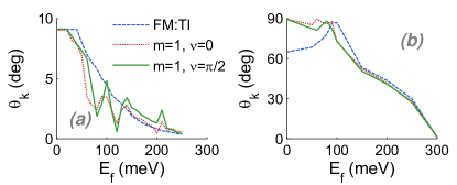
Finally, we study electro-optic switching effects as a function of Fermi energy. In Fig. 8(a), is shown as a function of Fermi energy . All values are shown at the at which occurs for in the low energy regime (see Fig. 4). Similarly Fig. 8(b), is shown as a function of in the intermediate energy regime. Here for each magnetic texture is where the resonances induced by the Cu2OSeO3 film thickness occur in Fig. 5(a).
In Fig. 8(a), all three textures show distinct behavior. While for the FM:TI shows a monotonic decrease with increasing , the Néel type and Bloch type SkXs show somewhat oscillatory non-monotonic behavior. This can be explained as follows. In the present model for the FM:TI all the states above the gap are degenerate and free electron like. Hence decreases monotonically with . Whereas in case of the SkX:TI, the states just above the gap are non-degenerate and the bands are split. This leads to additional peaks and valleys in the DOS, which causes the sudden jumps in Fig. 8(a) as moves up in energy. Lastly as a function of differs for the Néel type and Bloch type SkXs because their density of states is different above the gap as shown in Fig. 2. These effects can be numerically heightened if is increased tenfold. The band-splittings in Fig. 2 for the two SkXs, then evolve into energy gaps where the SkXs have different Chern numbers in the gaps. This will lead to very distinct MOKE signatures as a function of .
These dependent non-monotonic effects are not seen in Fig. 8(b), where the MOKE resonances are induced by the Cu2OSeO3 thin-film. Here, the Néel type and Bloch type SkXs are indistinguishable, but they both differ from the FM:TI. at is much smaller for the FM:TI because nm is not optimal in this case. The FM:TI and SkX:TI show distinct differences only for low .
In summary, the MOKE from SkX-hosting thin-film B20 type compounds interfaced with TI structures displays rich physics with important device applications. High FOM is obtained from the low energy topological MOKE, the thin-film induced enhancement of MOKE, and the MOKE occurring at the high energy plasma frequency. The MOKE-FOM phase diagram shows that the low energy peaks below the TI’s bulk energy gap are large and independent of . For the thin-film induced resonance, the differential MOKE can be large for the FM and SkX states, which is useful for device applications. As is swept above the exchange gap of the surface state, decreases monotonically for FM:TIs, and it is distinctly oscillatory and non-monotonic for SkX:TIs. These distinguishing features are not seen for the thin-film induced MOKE resonance. With a large FOM, optical readout can lead to high density and high fidelity MO memory devices and electro-optic devices such as modulators and optical-isolatorsBi et al. (2013); Onbasli et al. (2016).
Acknowledgement: This work was supported by the NSF ECCS-1408168 Physical Mechanisms and Limits of Skyrmions for Information Processing and Storage and as part of the Spins and Heat in Nanoscale Electronic Systems (SHINES) an Energy Frontier Research Center funded by the U.S. Department of Energy, Office of Science, Basic Energy Sciences under Award #DE-SC0012670.
References
- Kukushkin and Timofeev (1996) I. Kukushkin and V. Timofeev, Advances in Physics 45, 147 (1996).
- Tse and MacDonald (2010) W.-K. Tse and A. H. MacDonald, Phys. Rev. Lett. 105, 057401 (2010).
- Tse and MacDonald (2011) W.-K. Tse and A. H. MacDonald, Phys. Rev. B 84, 205327 (2011).
- Arima (2008) T. Arima, Journal of Physics: Condensed Matter 20, 434211 (2008).
- Atmatzakis et al. (2018) E. Atmatzakis, N. Papasimakis, V. Fedotov, G. Vienne, and N. I. Zheludev, Nanophotonics 7, 199 (2018).
- Sessoli et al. (2015) R. Sessoli, M.-E. Boulon, A. Caneschi, M. Mannini, L. Poggini, F. Wilhelm, and A. Rogalev, Nature physics 11, 69 (2015).
- Vomir et al. (2016) M. Vomir, R. Turnbull, I. Birced, P. Parreira, D. A. MacLaren, S. L. Lee, P. Andre´, and J.-Y. Bigot, Nano letters 16, 5291 (2016).
- Woo et al. (2018) S. Woo, K. M. Song, X. Zhang, Y. Zhou, M. Ezawa, X. Liu, S. Finizio, J. Raabe, N. J. Lee, S.-I. Kim, et al., Nature Communications 9, 959 (2018).
- Jiang et al. (2017) W. Jiang, X. Zhang, G. Yu, W. Zhang, X. Wang, M. B. Jungfleisch, J. E. Pearson, X. Cheng, O. Heinonen, K. L. Wang, et al., Nature Physics 13, 162 (2017).
- Hansen (1990) P. Hansen, Journal of Magnetism and Magnetic Materials 83, 6 (1990).
- Suzuki et al. (1992) Y. Suzuki, T. Katayama, S. Yoshida, K. Tanaka, and K. Sato, Phys. Rev. Lett. 68, 3355 (1992).
- MANSURIPUR (2000) M. MANSURIPUR, Opt. Photon. News 11, 34 (2000), URL http://www.osa-opn.org/abstract.cfm?URI=opn-11-10-34.
- Mansuripur (1986) M. Mansuripur, Applied physics letters 49, 19 (1986).
- Challener (1995) W. A. Challener, Journal of Physics and Chemistry of Solids 56, 1499 (1995), ISSN 0022-3697, proceedings of the 1994 Conference on Magneto-optic Materials.
- Taussig et al. (2008) A. R. Taussig, G. F. Dionne, and C. A. Ross, Phys. Rev. B 77, 012407 (2008).
- Lairson and Clemens (1993) B. Lairson and B. Clemens, Applied physics letters 63, 1438 (1993).
- Van Engen et al. (1983) P. Van Engen, K. Buschow, R. Jongebreur, and M. Erman, Applied Physics Letters 42, 202 (1983).
- Egashira and Yamada (1974) K. Egashira and T. Yamada, Journal of Applied Physics 45, 3643 (1974).
- Reim and Weller (1988) W. Reim and D. Weller, Applied physics letters 53, 2453 (1988).
- De and Puri (2002a) A. De and A. Puri, Journal of Applied Physics 92, 5401 (2002a).
- De and Puri (2003) A. De and A. Puri, Journal of Applied Physics 93, 1120 (2003).
- Gross et al. (2018) I. Gross, W. Akhtar, A. Hrabec, J. Sampaio, L. Martínez, S. Chouaieb, B. Shields, P. Maletinsky, A. Thiaville, S. Rohart, et al., Physical Review Materials 2, 024406 (2018).
- Li et al. (2014) J. Li, A. Tan, K. Moon, A. Doran, M. Marcus, A. Young, E. Arenholz, S. Ma, R. Yang, C. Hwang, et al., Nature communications 5, 4704 (2014).
- Tolley et al. (2018) R. Tolley, S. Montoya, and E. Fullerton, Physical Review Materials 2, 044404 (2018).
- Luo et al. (2018) S. Luo, M. Song, X. Li, Y. Zhang, J. Hong, X. Yang, X. Zou, N. Xu, and L. You, Nano letters (2018).
- Rößler et al. (2006) U. Rößler, A. Bogdanov, and C. Pfleiderer, Nature 442, 797 (2006).
- Mühlbauer et al. (2009) S. Mühlbauer, B. Binz, F. Jonietz, C. Pfleiderer, A. Rosch, A. Neubauer, R. Georgii, and P. Böni, Science 323, 915 (2009).
- Tonomura et al. (2012) A. Tonomura, X. Yu, K. Yanagisawa, T. Matsuda, Y. Onose, N. Kanazawa, H. S. Park, and Y. Tokura, Nano letters 12, 1673 (2012).
- Yu et al. (2013) X. Yu, J. P. DeGrave, Y. Hara, T. Hara, S. Jin, and Y. Tokura, Nano letters 13, 3755 (2013).
- Yu et al. (2010) X. Yu, Y. Onose, N. Kanazawa, J. Park, J. Han, Y. Matsui, N. Nagaosa, and Y. Tokura, Nature 465, 901 (2010).
- Huang and Chien (2012) S. Huang and C. Chien, Physical review letters 108, 267201 (2012).
- Seki et al. (2012) S. Seki, X. Yu, S. Ishiwata, and Y. Tokura, Science 336, 198 (2012).
- Zhu et al. (2018) D. Zhu, W. Kang, S. Li, Y. Huang, X. Zhang, Y. Zhou, and W. Zhao, IEEE Transactions on Electron Devices 65, 87 (2018).
- Yu et al. (2016) G. Yu, P. Upadhyaya, X. Li, W. Li, S. K. Kim, Y. Fan, K. L. Wong, Y. Tserkovnyak, P. K. Amiri, and K. L. Wang, Nano letters 16, 1981 (2016).
- Mochizuki (2012) M. Mochizuki, Phys. Rev. Lett. 108, 017601 (2012).
- Mochizuki and Watanabe (2015a) M. Mochizuki and Y. Watanabe, Applied Physics Letters 107, 082409 (2015a).
- Romming et al. (2013a) N. Romming, C. Hanneken, M. Menzel, J. E. Bickel, B. Wolter, K. von Bergmann, A. Kubetzka, and R. Wiesendanger, Science 341, 636 (2013a).
- Nakatani et al. (2016) Y. Nakatani, M. Hayashi, S. Kanai, S. Fukami, and H. Ohno, Applied Physics Letters 108, 152403 (2016).
- White et al. (2012) J. S. White, I. Levatić, A. Omrani, N. Egetenmeyer, K. Prša, I. Živković, J. Gavilano, J. Kohlbrecher, M. Bartkowiak, H. Berger, et al., Journal of Physics: Condensed Matter 24, 432201 (2012).
- Koshibae et al. (2015) W. Koshibae, Y. Kaneko, J. Iwasaki, M. Kawasaki, Y. Tokura, and N. Nagaosa, Japanese Journal of Applied Physics 54, 053001 (2015).
- Schott et al. (2017) M. Schott, A. Bernand-Mantel, L. Ranno, S. Pizzini, J. Vogel, H. Béa, C. Baraduc, S. Auffret, G. Gaudin, and D. Givord, Nano Letters 17, 3006 (2017).
- Okamura et al. (2016) Y. Okamura, F. Kagawa, S. Seki, and Y. Tokura, Nature communications 7, 12669 (2016).
- Mochizuki and Watanabe (2015b) M. Mochizuki and Y. Watanabe, Applied Physics Letters 107, 082409 (2015b).
- Romming et al. (2013b) N. Romming, C. Hanneken, M. Menzel, J. E. Bickel, B. Wolter, K. von Bergmann, A. Kubetzka, and R. Wiesendanger, Science 341, 636 (2013b).
- Everschor et al. (2011) K. Everschor, M. Garst, R. Duine, and A. Rosch, Physical Review B 84, 064401 (2011).
- Zang et al. (2011) J. Zang, M. Mostovoy, J. H. Han, and N. Nagaosa, Physical review letters 107, 136804 (2011).
- Koshibae and Nagaosa (2014) W. Koshibae and N. Nagaosa, Nature communications 5, ncomms6148 (2014).
- Hsu et al. (2016) P.-J. Hsu, A. Kubetzka, A. Finco, N. Romming, K. von Bergmann, and R. Wiesendanger, Nature Nanotechnology 12, 123 (2016).
- Yin et al. (2016) G. Yin, Y. Li, L. Kong, R. K. Lake, C.-L. Chien, and J. Zang, Physical Review B 93, 174403 (2016).
- Yasuda et al. (2016) K. Yasuda, R. Wakatsuki, T. Morimoto, R. Yoshimi, A. Tsukazaki, K. Takahashi, M. Ezawa, M. Kawasaki, N. Nagaosa, and Y. Tokura, Nature Physics 12, 555 (2016).
- Hurst et al. (2015) H. M. Hurst, D. K. Efimkin, J. Zang, and V. Galitski, Physical Review B 91, 060401 (2015).
- Lu et al. (2010) H.-Z. Lu, W.-Y. Shan, W. Yao, Q. Niu, and S.-Q. Shen, Physical review B 81, 115407 (2010).
- Xia et al. (2009) Y. Xia, D. Qian, D. Hsieh, L. Wray, A. Pal, H. Lin, A. Bansil, D. Grauer, Y. Hor, R. Cava, et al., Nature Physics 5, 398 (2009).
- Susskind (1977) L. Susskind, Physical Review D 16, 3031 (1977).
- Hong et al. (2012) S. Hong, V. Diep, S. Datta, and Y. P. Chen, Physical Review B 86, 085131 (2012).
- Lado and Fernández-Rossier (2015) J. L. Lado and J. Fernández-Rossier, Physical Review B 92, 115433 (2015).
- Nagaosa and Tokura (2013) N. Nagaosa and Y. Tokura, Nature nanotechnology 8, 899 (2013).
- Hamamoto et al. (2015) K. Hamamoto, M. Ezawa, and N. Nagaosa, Physical Review B 92, 115417 (2015).
- Kanazawa et al. (2015) N. Kanazawa, M. Kubota, A. Tsukazaki, Y. Kozuka, K. Takahashi, M. Kawasaki, M. Ichikawa, F. Kagawa, and Y. Tokura, Physical Review B 91, 041122 (2015).
- Thouless et al. (1982) D. Thouless, M. Kohmoto, M. Nightingale, and M. Den Nijs, Physical Review Letters 49, 405 (1982).
- Kohmoto (1985) M. Kohmoto, Annals of Physics 160, 343 (1985).
- Eddrief et al. (2016) M. Eddrief, F. Vidal, and B. Gallas, Journal of Physics D: Applied Physics 49, 505304 (2016).
- Jackson et al. (1985) A. Jackson, A. Jackson, and V. Pasquier, Nuclear Physics A 432, 567 (1985).
- Münzer et al. (2010) W. Münzer, A. Neubauer, T. Adams, S. Mühlbauer, C. Franz, F. Jonietz, R. Georgii, P. Böni, B. Pedersen, M. Schmidt, et al., Physical Review B 81, 041203 (2010).
- Yu et al. (2012) X. Yu, N. Kanazawa, W. Zhang, T. Nagai, T. Hara, K. Kimoto, Y. Matsui, Y. Onose, and Y. Tokura, Nature communications 3, 988 (2012).
- Argyres (1955) P. N. Argyres, Phys. Rev. 97, 334 (1955).
- Feil and Haas (1987) H. Feil and C. Haas, Phys. Rev. Lett. 58, 65 (1987).
- De and Puri (2002b) A. De and A. Puri, Journal of Applied Physics 91, 9777 (2002b).
- Abe and Suwa (2004) M. Abe and T. Suwa, Phys. Rev. B 70, 235103 (2004).
- Ferreira et al. (2012) A. Ferreira, N. M. R. Peres, and A. H. Castro Neto, Phys. Rev. B 85, 205426 (2012).
- Tymchenko et al. (2013) M. Tymchenko, A. Y. Nikitin, and L. Martín-Moreno, ACS nano 7, 9780 (2013).
- Miller et al. (2010) K. H. Miller, X. S. Xu., H. Berger, E. S. Knowles, D. J. Arenas, M. W. Meisel, and D. B. Tanner, Phys. Rev. B 82, 144107 (2010).
- Bi et al. (2013) L. Bi, J. Hu, P. Jiang, H. S. Kim, D. H. Kim, M. C. Onbasli, G. F. Dionne, and C. A. Ross, Materials 6, 5094 (2013), ISSN 1996-1944.
- Onbasli et al. (2016) M. C. Onbasli, L. Beran, M. Zahradník, M. Kučera, R. Antoš, J. Mistrík, G. F. Dionne, M. Veis, and C. A. Ross, Scientific reports 6, 23640 (2016).