Measurements and simulations of athermal phonon transmission from silicon absorbers to aluminium sensors
Abstract
Phonon reflection/transmission at the interfaces plays a fundamental role in cryogenic particle detectors, in which the optimization of the phonon signal at the sensor (in case of phonon-mediated detectors) or the minimization of the heat transmission (when the detection occurs in the sensor itself) is of primary importance to improve sensitivity. Nevertheless the mechanisms governing the phonon physics at the interfaces are still not completely understood. The two more successful models, Acoustic Mismatch Model (AMM) and Diffuse Mismatch Model (DMM) are not able to explain all the accumulated experimental data, and the measurement of the transmission coefficients between the materials remains a challenge. Here, we use measurements of the athermal phonon flux in aluminium Kinetic Inductance Detectors (KID) deposited on silicon substrates following a particle interaction to validate a Monte Carlo (MC) phonon simulation. We apply the Mattis-Bardeen theory to derive the phonon pulse energy and timing from the KID signal and compare the results with the MC for specular (AMM) and diffuse (DMM) reflection, finding a remarkable good agreement for specular, while diffuse reflection is clearly disfavoured. For an aluminum film of 60 nm and a silicon substrate of 380 m, we obtain transmission coefficients Si-Al in the range [0.3 - 0.55] and Si-Teflon in the range [0.1 - 0.15].
I Introduction
Phonon-mediated cryogenic detectors using massive absorbers are a mature technology extensively employed in rare event physics experiments, like neutrinoless double beta decay () searches 1 (see for example CUORE 2, CUPID-0 3, LUMINEU 4, AMoRE 5…) and dark matter direct detection experiments 6, 7 (EDELWEISS 8 , SuperCDMS 9, CRESST 10…). Generally the working temperature is 100 mK and the most common phonon sensors are Neutron Transmutation Doped (NTD) Ge or ion-implanted Si thermistors 11, which are glued or bonded to the detector surface and depending on the gluing characteristics are more or less sensitive to the ballistic component, or Transition Edge Sensors (TES) 12, which usually are sensitive to the ballistic phonons. Recently other kinds of sensor are being developed, as Metallic Magnetic Calorimeters (MMC) 13 or Kinetic Inductance Detectors (KIDs, the ones used in this work) 14. In all cases, low-threshold detection and/or an identification of the event topology (multi-site event, bulk vs surface…) and nature of the interacting particle (, , nuclear recoil…) are mandatory, and hence a good understanding of the phonon transport mechanism and heat losses in the interfaces is fundamental. On the other hand, a good understanding of these processes could also be useful to mitigate the effects of unwanted phonon-mediated signals. This is the case of cryogenic bolometers employed for CMB measurements in space, which are severely affected by cosmic rays 15, 16, and superconducting qubits, where phonons generated by cosmic rays and natural radioactivity can modify the qubit state 17, 18.
Monte Carlo (MC) simulation of particles transport and interactions in matter is one of the basic ingredients for the design of a particle detector and the detection efficiency calculation. In particular the GEANT4 package 19, initially developed for high energy Physics, now is used by a much wider community, including astroparticle, space and medical Physics. Nevertheless, at the level of phonon physics, despite the fundamental role they play in the energy collection in cryogenic bolometers, there is no generalized use of this analysis tool. Recently GEANT4 has incorporated condensed matter physics elements as phonon and electron-hole pairs, essential for a more complete understanding of a cryogenic detector. The code was first developed by the CDMS cryogenic Dark Matter experiment 20 and subsequently integrated into GEANT4 as a general open-source package called G4CMP (GEANT4 Condensed Matter Physics) 21, 22. It has been validated for germanium, reproducing quite accurately the results of some experiments using heat pulses (produced for example by a focused laser beam ) to excite ballistic phonons 23, and also giving a good description of the CDMS detectors: Ge cylinders with interleaved ionization and grounded phonon electrodes coupled to tungsten TES to read the phonon signal. The MC simulation reproduces the arrival time of the ballistic phonons into the TES and the energy partition between the phonon and charge 24, 25.
A correct treatment of the phonon scattering/transmission at the interfaces is a main ingredient of the simulation when the sensitive area is a small fraction of the total detector surface. Nevertheless, phonon scattering at the interfaces is still an open question, and there is no general agreement about the model to describe the experimental data, being the most well established ones the acoustic mismatch model (AMM) and the diffuse mismatch model (DMM) 26. AMM, which proposes specular reflection on the interface in analogy with the Snell’s law for light, has been very successful at low temperatures 27, while DMM, in which phonons undergo diffuse reflection, is sensitive to surface roughness and preferred at temperatures above 1 K 28. G4CMP include a basic implementation of the phonon reflection mechanism based on these models in which a phonon in the boundary undergoes a reflection (specular for the AMM model or diffuse (Lambertian) for the DMM model), or is transmitted through the boundary with a certain probability given by a transmission coefficient, but the experimental determination of the phonon transmission coefficients at the interfaces is a hard task, and currently large uncertainties exist.
In this work we apply the G4CMP package to model two prototypes of the CALDER project 29, that is part of the R&D activities under development for the future upgrade of CUORE (the first ton-scale cryogenic detector in operation looking for 2). The CALDER goal is to develop large-area high-sensitivity light detectors able to measure the very weak Cherenkov light that follows a event and allow to distinguish it from other backgrounds. The light is detected by superconducting KIDs of few mm2 of active area deposited on a substrate of several cm2 that acts as a light absorber and generates phonons that will be absorbed in the superconductor and produce the signal. The main advantage of using KIDs for this study is that their response can be modeled as a function of measurable parameters of the Mattis-Bardeen theory, so we are able to estimate the total energy transformed into quasi-particles, and make a direct comparison with the MC results. In addition, the small fractional area covered by the sensors with respect to the total absorber one enhances the influence of the phonon reflection/transmission model in the final results.
We apply the G4CMP package to a silicon wafer read by one or several KIDs. Comparing the simulation results with our data we found a notable agreement for the AMM model, and we are able to estimate the transmission coefficients at the interfaces Si-Al () and Si-Teflon. The results that we present here can be extended to other kind of detectors based on thin Al sensors.
The structure of the paper is as follows: Section II presents a brief description of the main physics ingredients included in the MC code and the parameters used in our implementation. Section III describes the general aspects of our detectors, experimental setup, data analysis, and the specific experimental configurations simulated. The details of the MC simulation are outlined in Section IV, while in Section V we compare the MC results with the experimental data and make an estimation of the relevant parameters. Finally, we present the summary in Section VI.
II Phonon physics
In this section we describe the basic phonon physics mechanisms implemented in the MC simulation, referring to 21, 30 for a more complete description. Table 1 reports the numerical parameters used in our simulation, whose meaning is given in the following.
In a phonon-mediated cryogenic detector, particles (optical photons in our case) hitting the absorber produce optical phonons that decay promptly to the acoustic branch, producing an athermal population of high energy. The interaction length of these energetic phonons is very short, so they propagate quasidiffusively, with numerous changes in direction and polarization mode as they decay to lower energy states. When the phonon energy drops sufficiently, its mean free path becomes larger than the dimensions of the crystal and it propagates following almost straight lines at the speed of sound in the material, a state that we call ballistic. If the dimensions of the sensor are small compared to the absorber size, as for CALDER detectors, ballistic phonons can undergo a large number of reflections at the substrate faces before reaching the KID, where they have a certain probability of being absorbed, or escaping detection (i.e., they are thermalized in the substrate or absorbed at the supports or the feedline).
| Symbol | Parameter description | Value | Ref |
|---|---|---|---|
| d | density | 2.33 g/cm3 | 31 |
| elastic constant | 165.6 GPa | 32 | |
| elastic constant | 63.9 GPa | 32 | |
| elastic constant | 79.5 GPa | 32 | |
| 2nd order elastic constant | -42.9 GPa | 31 | |
| 2nd order elastic constant | -94.5 GPa | 31 | |
| Lamé constant | 52.4 GPa | 31 | |
| Lamé constant | 68.0 GPa | 31 | |
| DOS(L) | density of states L | 0.093 | 33 |
| DOS(FT) | density of states FT | 0.376 | 33 |
| DOS(ST) | density of states ST | 0.531 | 33 |
| anharmonic decay rate | 7.41s4 | 34 | |
| isotopic scattering rate | 2.43s3 | 34 | |
| Debye frequency | 15 THz | 32 | |
| pair-breaking efficiency | 0.57 | 35 | |
| fraction of phonons tracked | 0.02 | ||
| maximum number of reflections | 1000 | ||
| Si-Al transmission coefficient | [0.1 - 1] | ||
| Si-Teflon transmission coefficient | [0.1 - 1] |
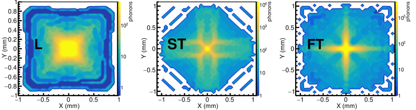
Phonon tracking in crystalline structures strongly differs from the usual particle propagation in GEANT code because (1) an acoustic phonon can be in three different polarization states, one longitudinal (L) and two transversal, fast (FT) and slow (ST), with different velocities for every state; (2) the direction of energy propagation, that occurs along the group velocity vector, , where is the phonon frequency, does not flow in general parallel to the wavevector direction k. This fact, that depends on the crystal lattice symmetry and physical properties (mainly the elastic constants), causes the phonons to travel in preferred directions along the crystal, a phenomenon known as “phonon focusing” 36, 37. Silicon has a face centered cubic crystal structure for which we expect quasi isotropic transport for longitudinal phonons, but highly anisotropic one for the transversal modes. To check that the caustics are correctly generated in our code we perform a simulation starting with low energy phonons of around 0.1 THz produced in a small spot at the surface of the Si wafer. Phonons of this frequency are ballistic in Si, so they propagate along an almost unchanged trajectory and polarization state until they reach the opposite face, forming the characteristic phonon focusing structures observed in Si by laser-beam experiments 38 (see Fig. 1).
The phonon propagation in the crystal is mainly governed by two processes:
-
1.
isotopic scattering: when the substrate is composed of different isotopes, as it is usually the case, there is a disruption in the propagation path that causes the phonon to scatter off and change direction with no energy loss. The energy-dependent rate is modeled as , where depends on the material (see Table 1) and is the phonon frequency. The single scattering process depends on the inner product of the polarization vectors of the initial and final phonons, but the total expected rate is isotropic. Thus, the isotropic approximation in which the scattered phonon has random direction and polarization distribution according to the density of states (DOS) is pretty accurate after several scatters and much less time consuming;
-
2.
anharmonic decay: due to nonlinear terms in the elastic coupling between adjacent lattice ions, a phonon spontaneously splits into two (or more) lower frequency ones, with a rate that depends on the phonon frequency as , where is a material-dependent constant (see Table 1). A complete treatment of the scattering process is computationally too expensive, so usually the isotropic approximation, in which only L phonons can decay via LL+T and LT+T processes, is adopted.
As said before, there is not yet a complete understanding of the mechanisms that govern the phonon physics at the interfaces. Ideally phonons reflect and transmit conserving the energy and the component of k parallel to the interface, but polarization conversion can occur, being in general three reflected waves (trirefringence) and at most two transmitted ones (birefringence) 39. The AMM and DMM models are the most extended but none of them is sufficient to entirely explain the experimental data.
III Phonon-mediated kinetic inductance detectors
KIDs operation principle is based on the properties of a superconducting film biased with AC (microwave) current. The inertia of Cooper pairs to momentum change produces an additional inductance, called kinetic inductance (LKI), which depends on the density of Cooper pairs, and that can be measured embedding the superconductor in a resonant RLC circuit with resonant frequency . An energy release larger than twice the superconductor gap (about 200 eV for thin Al films) breaks Cooper pairs into quasiparticles, modifying both the residual resistance due to quasiparticles (the only dissipative term in the RLC resonant circuit) and the inductance due to Cooper pairs and changing the amplitude and phase of a microwave signal transmitted past the circuit. Slightly modifying the capacitance of every resonator we can make them resonate at close but different frequencies, and in that way many of them can be read with the same line.
The detector used in this work follows a Lumped Element KID (LEKID) design 40 that uses a separate meander section (inductor) and an interdigital capacitor to form a resonator coupled (inductively or capacitively) to a Coplanar Waveguide (CPW) for excitation and readout. They are fabricated at Istituto di Fotonica e Nanotecnologie of CNR (Rome). They are pattered by electron beam lithography in a 60 nm Al film deposited by electron-gun evaporator on a thin (300 m) high-resistivity Si (100) substrate 41, 42. In order to reduce the thermal quasiparticles population we operate the detector well below the Al critical temperature. The Si wafer is fixed to a copper holder by small Teflon supports that act as thermal link to the heat sink while the holder is anchored to the coldest point of a dilution refrigeration, at a base temperature of about 20 mK.
KIDs are excited with a fixed-frequency signal typically in the few GHz range. After transmission through the device, the signal is amplified by a CITLF4 SiGe cryogenic low noise amplifier (with noise temperature T7 K) operated at 4 K and the rest of the electronics are at room temperature 29.
The signal transmitted through the feedline can be written as a function of the frequency as follows:
| (1) |
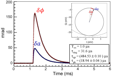
where is the forward scattering amplitude in the standard scattering matrix representation, I and Q indicate real and imaginary part of and is the quality factor of the resonant circuit, which is given by the addition in parallel of the coupling quality factor (that account for losses through the coupling) and the internal quality factor (dissipation due to quasiparticles and all other losses), so that . When sweeps around the resonance, the signal traces out a circle in the IQ plane of diameter equal to (see inset of Fig. 2). We determine the circle center and radius, taking into account distortions introduced by the power stored in the resonator and possible impedance mismatches 43, to translate the I(t) and Q(t) components into phase (t) and amplitude (t) variations relative to the center of the resonance loop (calibration).
Once the resonance is calibrated we choose the most sensitive frequency (or frequencies, in the case of reading several KIDs through the same line) and excite the resonators at an adequate power level 44. We run an amplitude threshold trigger algorithm on the continuously acquired signals to capture particle passages through the detector, and register a window of configurable length around the position of each trigger. Fig. 2 shows a typical response to a 36 keV energy deposit in the Si substrate. The component usually features much better signal-to-noise ratio (SNR) than (t), so in the following we use only this signal.
III.1 Phonon time constant
Athermal phonons arrive to the KIDs with a characteristic time distribution that depends on the detector material and geometry. In general it can be modeled by two time constants, accounting for the pulse rise () and decay (), so the number of phonons at the KID can be written as:
| (2) |
When , as in the case of the detectors analyzed in this work, the expression 2 can be approximated by a single exponential with constant .
In order to infer from the KID signal, we have to disentangle the contribution of other temporal constants: (1) at the KID phonons break Cooper pairs and generate quasiparticles with a probability given by the pair-breaking efficiency (see Tab. 1), which recombine again into Cooper pairs with lifetime . The recombination rate depends not only on superconductor properties, but also on the quasiparticle density, and consequently also on temperature and microwave power ()45; (2) the factor determines the time constant at which the power dissipation decays as , hence high- resonators are more sensitive but are also slower. The temporal evolution of the signal is a convolution of these effects:
| (3) |
where is the pulse integral and its expression is derived in the next section.
As we explain in next section, we excite the substrate by a LED pulse whose duration is of the order of few s, so the final waveform results from the convolution of Eq. 3 with a rectangular function of length .
For every acquired signal we fit the pulse evolution to the pulse shape described above, fixing to the value corresponding to the measured factor. In this way we obtain that we compare with the MC results. Superimposed to the pulses of Fig. 2 we show the results form the fit for the and signals.
III.2 Response to energy absorption
We can relate the energy release in the substrate to the energy absorbed at every resonator through an efficiency factor , so that . The efficiency can be factorized as , where depends on the geometry of the detector and the transmission coefficients at the interface, and it is the parameter that we shall extract from the MC simulation, and is the pair-breaking efficiency in Al, which we take as 0.57 35. Now, in Eq. 3 represents the overall change in corresponding to an increment in the quasi-particle population =/, that can be calculated from the Mattis-Bardeen theory in the thin film limit. After some analytical approximations 46 we can write:
| (4) |
where is the single spin density of states at the Fermi level (1.72 eV-1 m-3 for Al 14) multiplied by the active volume of the resonator, is the fraction of kinetic inductance , is the effective temperature of the quasiparticle system, larger than the sink temperature due to , and is a dimensionless factor given by the Mattis-Bardeen theory. The parameters , , and are measurable quantities for a given , therefore from the pulse fit we can obtain and determine through Eq. 4 the efficiency of every pixel in order to compare with the MC results.
III.3 Experimental configurations
We study two different detector configurations with different KID characteristics and layout.
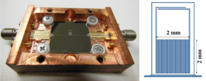
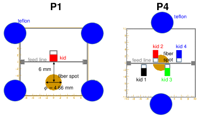
The first prototype (P1 in the following) consists of a single KID lithographed on a thick Si substrate with a size of 22 cm2. Fig. 3 shows a picture of the detector mounted in the copper holder (left panel) and a schematic design of the single KID (right panel). The inductor section is a meander of 30 strips of 62.5 m2 mm, with gap of 5 m between them, and the capacitor is composed of only two fingers. The total active area is 4.0 mm2, excluding the gaps and including the active region that connects the inductor to the capacitor. The feedline is a 72 m width CPW that cuts across the Si substrate from side to side. The pixel and feedline are made of 60 nm thick Al. Four cylindrical Teflon supports, one at every corner of the substrate, fix the detector to a copper holder that is anchored to the cryostat. The contact area between Si and Teflon is lower than 3 mm2 at every support. For detailed results of this prototype, see 44.
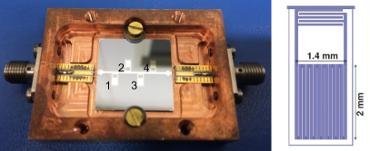
In the second prototype, that we label as P4 (see Fig. 4), the wafer is thick and there are four Al KIDs with an inductive meander made of 14 connected strips of 80 m2 mm closed by a capacitor made of 5 interdigitated fingers of 1.4 mm50 m. The active area of the single pixel is mm2. The feedline is a 420 m width and 60 nm thick CPW.
Compared to P1, P4 has smaller contact area between Si and Teflon, as it is held by only two supports at opposite edges in the middle of the substrate. The contact area at every support is about 3 mm2, so the total interface Si-Teflon is halved with respect to P1. In turn, the feedline is 6 times wider.
| Prototype | coupling | Tc | KID | Source | |||||||||
| [K] | [V] | [%] | [dBm] | [k] | [k] | [k] | [s] | pos [mm] | [mm] | [s] | |||
| P1 | inductive | 1.1800.020 | 1793 | 2.54 0.90.26syst | -76.8 | 1 | 149 | 2301 | 159 | 18.2 | (0,-6) | 4.66 | 10 |
| P4 | capacitive | 1.3000.025 | 1974 | 2.140.040.27syst | -79.1 | 1 | 18.6 | 69.7 | 25.4 | 2.23 | (0,0) | 4.66 | 1 |
| 2 | 38.4 | 99.6 | 62.4 | 4.59 | |||||||||
| 3 | 138 | 899 | 162 | 16.4 | |||||||||
| 4 | 266 | 407 | 772 | 31.6 | |||||||||
We operate both prototypes as described at the beginning of this section. The first step is to select the excitation power . High powers feature in general a better SNR, as the noise in our setup is dominated by the amplifier and goes with , but as we raise the resonances show an increasing distortion and the relationship of Eq. 4 is not longer valid 44. Therefore we perform a power scan and select the largest before distortion.
For every prototype we measure the parameters that enter in Eq. 4 and report their values at the selected in Table 2. The , and factors are computed by fitting the resonance circle as described in 43. We determine the critical temperature (that for thin films depends on thickness and other parameters, as the quality of the deposition) during the cooling-down and infer from BCS theory. Then, we compute from the resonant frequency shift as we increase the thermal quasiparticle density by increasing the base temperature of the system. We fit the resulting curve to the Mattis-Bardeen theory prediction 47, keeping fixed in the fit. For the P4 prototype we average the results of the four resonators.
The detectors are illuminated on the back of the substrate by an optical fiber coupled to a fast warm LED (400 nm). The LED equivalent energy is calibrated with a photomultiplier, and the calibration is checked at very low intensity by photon counting Poisson statistics 48. In Table 2 we report also the source position with respect to the center of the substrate, the diameter of the illuminated spot () and the optical pulse duration.
We take LED pulses for every configuration. In order to improve the SNR we apply a software low-pass filter with 100 kHz cut-off whose effect is included in the pulse fitting. Finally, we average the pulses and perform a fit as described in Sec. III.1 to obtain and . We report the results for each KID in Table 3.
| Prototype | KID | [%] | [s] |
|---|---|---|---|
| P1 | 1 | 13.31.1 | |
| P4 | 1 | 2.90.3 | |
| 2 | 6.70.7 | ||
| 3 | 6.20.7 | ||
| 4 | 2.70.4 |
The error in is dominated by the systematic error in and . For , in addition to the statistical error of the fit, we estimate a systematic one by starting from different sets of initial fit parameters and by taking pulses with different ranging from 1 to 10 s. The /NDF of the fits range between 1 and 3.5 for all the KIDs except for KID3, for which we obtain values between 4 and 6.8. In P4 prototype there is a very small (200 m) rightwards shift of the kids layout with respect to the center of the substrate. It is not appreciable in Fig. 4, but it is responsible for the slight (7%) larger efficiency of KIDs 1 and 2 with respect to KIDs 3 and 4, as they are slightly closer to the source. The simulation also includes the shift, so we expect to observe this small effect in the MC results as well.
IV G4CMP MC implementation
The G4CMP package simulates: (1) the generation of acoustic phonons and electron-hole pairs in a material after an energy deposition; (2) their propagation in the media, anisotropic according to the material elastic constants for phonons and driven by an electric field for the charge; (3) the two principal phonon scattering processes described in Sec. II with isotropic approximation; and (4) a simplified implementation of the reflection and transmission mechanisms at interfaces, in which the multirefringence is not considered: the phonon is transmitted through the boundary with a probability given by the transmission coefficient, or it is reflected back, following a specular reflection for the AMM model or a Lambertian one for DMM. So, in the current implementation no mode conversion occurs.
In our simulation, as no electric field is applied to the detector, the charge is not taken into account and all the energy of the interaction goes to the phonon channel. Following a photon absorption in the Si substrate, acoustic phonons are generated isotropically along the incident particle track. The energy distribution of the primordial phonons is unknown, nevertheless their effects are wiped out after the quasidiffusion stage, so we take the Debye energy (62 meV in Si) as starting point and select the polarization L, FT or ST randomly according to the DOS in the material. The history of every phonon is followed recording its polarization, and k until one of the following conditions is verified: (1) it is absorbed in Al (KIDs or feedline) or Teflon; (2) its energy drops below ; (3) a predefined number of reflections is reached.
We simulate a simplified geometry of the detector with four main components: Si wafer, Teflon supports, the feedline and the KIDs, both made of Al (see Fig. 5). For the sake of keeping the simulation computing time at a reasonable level, only a certain fraction of the phonons are tracked (see Tab. 1) and the final results are scaled with this value.
In order to determine the effect of the reflection model and transmission coefficients we generate a batch of simulations spanning and from 0.1 to 1, for both models. It is worth mentioning that the code does not implement phonon propagation in Al, so a phonon absorbed in the KIDs generates a signal with probability or is killed. Hence, (1-) include the probability of a phonon to enter the Al and to be reflected back to the Si substrate.
A single simulation event starts with the generation of about 104 optical photons (=400 nm), uniformly distributed at the 4.66 mm diameter fiber spot, that are stopped in the first micron of the Si substrate at the opposite face to the KIDs. The spot is centered in the middle of the substrate in P4 simulation, while for P1 it is shifted 6 mm far from the KID in vertical direction, and the photons are distributed in time according to a square pulse of duration (see Table 2). For every configuration we generate between 20 and 50 single events. The outputs of the simulation are the time, energy, position and polarization of every phonon absorbed in the Teflon, the feedline or the KIDs.
V Results and discussion
For each fiber event in the wafer we construct the phonon pulse evolution for every time and integrate it to obtain the total energy absorbed in the simulation at every KID, that we denote as Eph. Then, we scale with the number of tracked phonons and the pair-breaking efficiency to calculate the absorbed energy, and divide by E to obtain the efficiency in a single KID as
| (5) |
Fig 6 displays one of such events for AMM model, =0.36 and =0.4 for both prototypes. The simulation does not include resonator-related time constants (, ), so the pulse shape is described by Eq. 2. The rise time of the phonon pulses is around one order of magnitude smaller than the decay time, so we consider only one time constant calculated as /2.2, where is the 90th minus the 10th percentile of the phonon distribution.
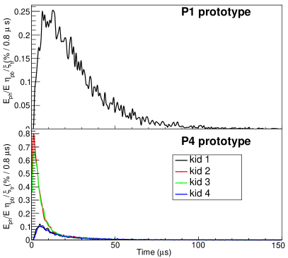
We observe no substantial variations in arrival time among the three polarizations, despite their different velocity (9000 m/s longitudinal, 5400 m/s for the transversal modes) since modes are highly mixed as a consequence of the scattering processes. For example, for the P1 pulse in Fig. 6 we obtain =(21.3, 21.3, 21.0) s for (L, FT, ST) components separately and =21.2 s for the three modes together.
The choice for the parameter is not of great importance in the final results: for the configurations with low values of the transmission coefficients (0.2, 0.1), only 1-3% (0.1-0.4%) phonons undergo more than 200 (500) reflections. For values of and around 0.4, the percentages are 0.5-1% (0.05-0.1%).
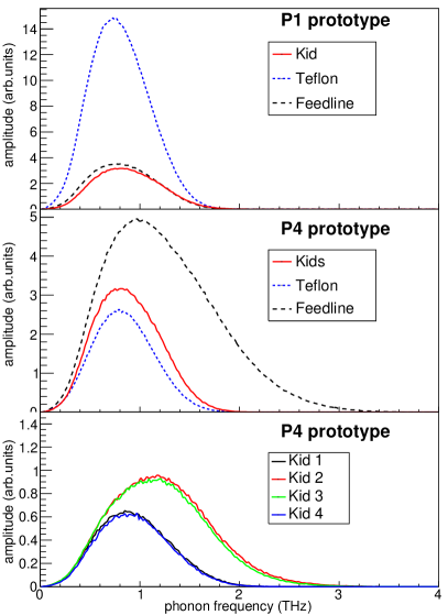
We also study the amount of phonon absorption at every material as a function of phonon frequency and show the results in Fig. 7 for the same configuration as Fig. 6. The geometric differences among the two prototypes described in Sec. III.3 (more Teflon in P1, 6 times wider feedline in P4) are clearly reflected in the simulation: while for P1 most of the phonons are absorbed in Teflon (about 60% of the total), in P4 the element that is taking the major part is the feedline (55%), followed by the KIDs (28%) and then the Teflon (%). The maximum of the distributions are at phonon frequencies between 0.7 and 0.9 THz and they are slightly asymmetric, with positive skewness. When the origin of the phonon pulse is close to the absorbing element, as for the feedline and KIDs 2 and 3 in P4, the asymmetry is more pronounced with a longer tail to higher frequencies.
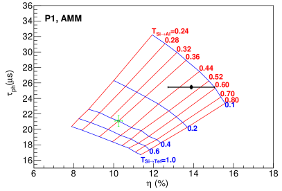
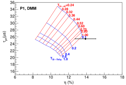
Finally, in Figs. 8 and 9 we compare the MC results with the experimental data. The red (blue) lines correspond to simulations with constant values of the () coefficient, while the points are taken from Table 3. In order to estimate a systematic error associated to the simulation we have identified the most sensitive parameters of the model to be the decay constants and and the elastic constants , and . We have considered a variation of 5% for the elastic constants 49, 50, 51 and 20% for the decay constants and calculated the variation in and for some simulated configurations. The result for AMM model, =0.36, =0.4 is 3% in and 2% in (green lines in Fig. 8). Similar results are obtained for other configurations. As regards the fraction of tracked phonons , increasing it from 2% up to 20% produces an error below 0.2%.
For P1, with one single KID, phonon pulses are faster and more energetic for larger values. When we increase instead, they are also faster, but less energy is collected, as phonons are lost in Teflon. This rule no longer holds true when more than one KID is competing for the same energy deposition, as it is the case of P4: the sensors far from the source (KID1 and KID4 in Fig. 9) reverse behavior, and the collected energy is lower for larger values of because it is being more quickly absorbed in the near KIDs and the feedline. The small shift in the KIDs position towards the right side of the wafer in P4 is also noticeable in the simulation and results in larger energy depositions in KID1 and KID2 compared to those of KID3 and KID4.
.
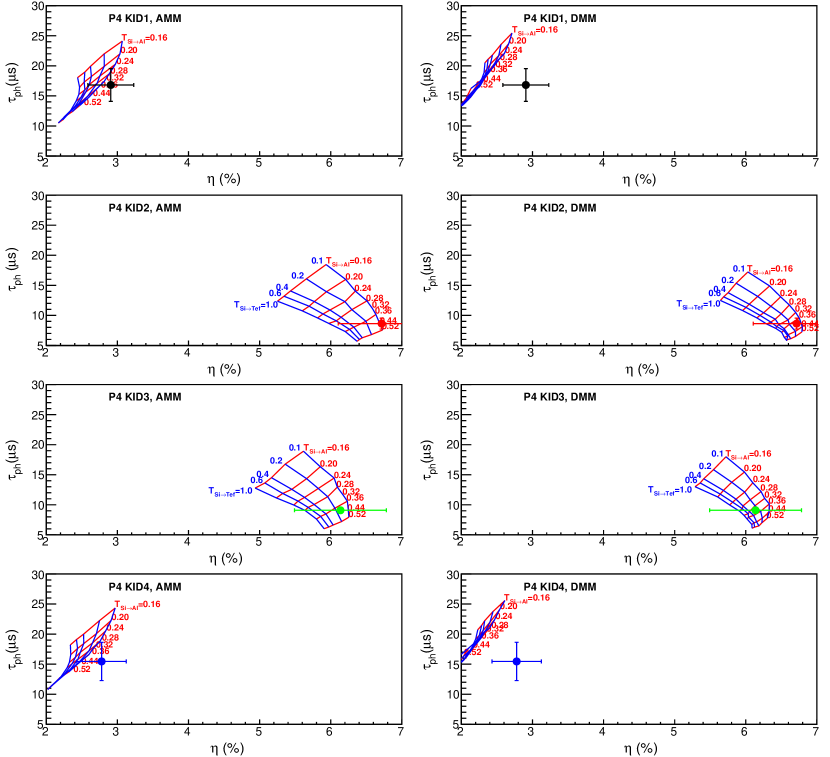
In general, simulations with DMM model produce slower and less energetic phonon pulses than those with AMM, except when KIDs are very close to the phonon source, as it is the case of KIDs 2 and 3 in P4. An explanation for this behaviour can be found in the very different propagation patterns that phonons follow once they enter the ballistic regime for specular or diffusive reflection. In our geometry we observe a much larger density of phonon tracks in the central part of the wafer for the AMM simulation rather than for DMM. The origin of this different distribution could be, as pointed out by some authors 52, that phonon caustics survive up to some degree with the specular reflection while a more homogeneous distribution of phonons is expected for a Lambertian reflection For our geometry, the larger concentration of phonons in the central part of the wafer results in a more effective energy collection at the KIDs than in Teflon.
We obtain a consistent picture between data and simulation for both prototypes for AMM model, while our experimental data cannot be modelled considering only diffuse reflection, unless extreme values of the transmission coefficients are introduced. In the case of P1 (the most sensitive probe for the reflection model, as the energy deposition is far away from the KID), for the same transmission coefficients, the DMM model produce phonon pulses between 2 and 4 s slower. This corresponds to between 10 and 20 times our experimental uncertainty. Our simulation with DMM model is not able to produce so fast an energetic phonon pulses as the ones we have measured for this setup, unless a transmission coefficient of almost 1 is considered for .
The range of values of that best describe the experimental data is [0.30-0.55]. In the case of , P1 data points to the region [0.1-0.15], nevertheless the P4 simulations do not impose a large constraint, as in general the whole range agrees with the experimental point at 1 error as a result of the reduced Si-Teflon interface. At a closer look, the AMM P4 simulation could be affected by a systematic bias: in the MC less energy is collected at the KIDs far from the source (KID1 and KID4) with respect to the measurement. This distance-dependent bias could suggest a deficiency of the model that appears when the number of phonon reflections is large. This could be due to the simplification of the reflection mechanisms in the simulation, that currently do not include mode conversion, or other phenomena non considered in the present implementation. For example, a slight dependence of the transmission coefficients with phonon frequency would result in distinct absorption for far and near KIDs, as the phonon frequency distribution is different (see Fig. 7). A larger substrate and/or a different KID layout would be necessary to test this conjecture.
It is worth noting that in general we expect the phonon transmission coefficient to be dependent on the thickness for thin films. The experimental data presented here correspond to an Al thickness of 60 nm, and so does the transmission coefficient that we have determined. Future measurements with different films will allow us to study this dependency.
VI conclusion
We have implemented a phonon MC simulation based on the G4CMP extension of the GEANT4 code and applied it to model phonon-mediated cryogenic detectors with thin Si absorbers and Al KID readout, clamped by Teflon supports to a dilution unit at about 20 mK. We have performed two different experiments with different geometries and KID layouts and we have compared the results with those of the MC simulations, considering two different reflection mechanisms at the interfaces (a specular reflection based on the AMM model and a diffuse one for the DMM model) and transmission coefficients spanning form [0.1-1] for the Si-Teflon and Si-Al interfaces. We found a good agreement for transmission coefficients Si-Al in the range [0.3-0.55] and Si-Tef in the range [0.1-0.15] for AMM model, while the simulation with diffuse reflection based on the DMM model does not provide a realistic description of our data. The Si-Al result is valid for an Al film with a thickness of 60 nm. We observe also a hint of a systematic bias in our simulation when the number of phonon reflections is large: simulated phonon pulses are less energetic than data. In the future we will further investigate this issue with larger detectors. The results that we have presented are applicable to other cryogenic detectors with thin Al sensors.
Acknowledgments
This work was supported by the European Research Council (FP7/2007-2013) under Contract No. CALDER No. 335359 and by the Italian Ministry of Research under the FIRB Contract No. RBFR1269SL. The authors thanks the personnel of INFN Sezione di Roma for the technical support, in particular M. Iannone.
References
- Dell’Oro et al. [2016] S. Dell’Oro, S. Marcocci, M. Viel, and F. Vissani, Neutrinoless double beta decay: 2015 review, Adv. High Energy Phys. 2016, 2162659 (2016), eprint arXiv:1601.07512.
- Alduino et al. [2018] C. Alduino et al., First Results from CUORE: A Search for Lepton Number Violation via 0 Decay of 130Te, Phys. Rev. Lett. 120, 132501 (2018).
- Azzolini et al. [2018] O. Azzolini et al., First Result on the Neutrinoless Double- Decay of 82Se with CUPID-0, Physical Review Letters 120, 232502 (2018), eprint arXiv:1802.07791.
- Armengaud et al. [2015] E. Armengaud et al., Development and underground test of radiopure ZnMoO4 scintillating bolometers for the LUMINEU 02 project, J. Instr. 10, P05007 (2015).
- Lee et al. [2016] J. Y. Lee et al., A Study of Radioactive Contamination of Crystals for the AMoRE Experiment, IEEE Trans. Nucl. Sci. 63, 543 (2016).
- Goodman and Witten [1985] M. W. Goodman and E. Witten, Detectability of Certain Dark Matter Candidates, Phys. Rev. D31, 3059 (1985).
- Strigari [2013] L. E. Strigari, Galactic Searches for Dark Matter, Phys. Rept. 531, 1 (2013), eprint arXiv:1211.7090.
- Hehn et al. [2016] L. Hehn et al., Improved EDELWEISS-III sensitivity for low-mass WIMPs using a profile likelihood approach, Eur. Phys. J. C 76, 548 (2016).
- Agnese et al. [2018] R. Agnese et al., Results from the super cryogenic dark matter search experiment at soudan., Phys. Rev. Lett. 120, 061802 (2018).
- Angloher et al. [2016] G. Angloher et al., Results on light dark matter particles with a low-threshold CRESST-II detector, Eur. Phys. J. C 76, 25 (2016), eprint arXiv:1509.01515.
- McCammon [2005] D. McCammon, in Cryogenic particle detection, edited by C. Enss (Springer, Berlin, Germany, 2005).
- Irwin and Hilton [2005] K. D. Irwin and G. C. Hilton, in Cryogenic particle detection, edited by C. Enss (Springer, Berlin, Germany, 2005).
- Fleischmann et al. [2005] A. Fleischmann, C. Enss, and G. M. Seidel, in Cryogenic particle detection, edited by C. Enss (Springer, Berlin, Germany, 2005).
- Day et al. [2003] P. K. Day, H. G. LeDuc, B. A. Mazin, A. Vayonakis, and J. Zmuidzinas, A broadband superconducting detector suitable for use in large arrays, Nature 425, 817 (2003).
- Catalano et al. [2014] A. Catalano et al., Impact of particles on the Planck HFI detectors: Ground-based measurements and physical interpretation, A&A 569, A88 (2014), eprint arXiv:1403.6592.
- Catalano et al. [2016] A. Catalano, A. Benoit, O. Bourrion, M. Calvo, G. Coiffard, A. D’Addabbo, J. Goupy, H. Le Sueur, J. Macías-Pérez, and A. Monfardini, Maturity of lumped element kinetic inductance detectors for space-borne instruments in the range between 80 and 180 GHz, A&A 592, A26 (2016), eprint arXiv:1511.02652.
- Serniak et al. [2018] K. Serniak, M. Hays, G. de Lange, S. Diamond, S. Shankar, L. D. Burkhart, L. Frunzio, M. Houzet, and M. H. Devoret, Hot Nonequilibrium Quasiparticles in Transmon Qubits, Physical Review Letters 121, 157701 (2018), eprint 1803.00476.
- Grünhaupt et al. [2018] L. Grünhaupt, N. Maleeva, S. T. Skacel, M. Calvo, F. Levy-Bertrand, A. V. Ustinov, H. Rotzinger, A. Monfardini, G. Catelani, and I. M. Pop, Loss Mechanisms and Quasiparticle Dynamics in Superconducting Microwave Resonators Made of Thin-Film Granular Aluminum, Phys. Rev. Lett. 121, 117001 (2018), eprint arXiv:1802.01858.
- Agostinelli et al. [2003] S. Agostinelli et al., GEANT4 - simulation toolkit, Nucl. Instr. Meth. A 506, 250 (2003).
- Agnese et al. [2015] R. Agnese et al., Improved WIMP-search reach of the CDMS II germanium data, Phys. Rev. D92, 072003 (2015), eprint arXiv:1504.05871.
- Brandt et al. [2014] D. Brandt, R. Agnese, P. Redl, K. Schneck, M. Asai, M. Kelsey, D. Faiez, E. Bagli, B. Cabrera, R. Partridge, T. Saab, and B. Sadoulet, Semiconductor phonon and charge transport Monte Carlo simulation using Geant4 (2014), eprint arXiv:1403.4984.
- [22] R. Agnese, D. Brandt, M. Kelsey, and P. Redl, G4CMP - Geant4 add-on framework for phonon and charge-carrier physics, URL https://github.com/kelseymh/G4CMP.
- Brandt et al. [2012] D. Brandt, M. Asai, P. L. Brink, B. Cabrera, E. Couto e Silva, M. Kelsey, S. W. Leman, K. McArthy, R. Resch, D. Wright, and E. Figueroa-Feliciano, Monte Carlo Simulation of Massive Absorbers for Cryogenic Calorimeters, J. Low. Temp. Phys. 167, 485 (2012).
- Leman et al. [2011] S. W. Leman, K. A. McCarthy, P. L. Brink, B. Cabrera, M. Cherry, E. S. E. Do Couto, E. Figueroa-Feliciano, P. Kim, N. Mirabolfathi, M. Pyle, R. Resch, B. Sadoulet, B. Serfass, K. M. Sundqvist, A. Tomada, et al., Monte Carlo Comparisons to a Cryogenic Dark Matter Search Detector with low Transition-Edge-Sensor Transition Temperature, J. Appl. Phys. 110, 094515 (2011), eprint arXiv:1109.1198.
- McCarthy et al. [2012] K. A. McCarthy, S. W. Leman, A. Anderson, D. Brandt, P. L. Brink, B. Cabrera, M. Cherry, E. Do Couto E Silva, P. Cushman, T. Doughty, E. Figueroa-Feliciano, P. Kim, N. Mirabolfathi, L. Novak, R. Partridge, et al., Validation of Phonon Physics in the CDMS Detector Monte Carlo, J. Low. Temp. Phys. 167, 1160 (2012), eprint arXiv:1109.0551.
- Swartz and Pohl [1989] E. T. Swartz and R. O. Pohl, Thermal boundary resistance, Rev. Mod. Phys. 61, 605 (1989).
- Swartz and Pohl [1987] E. T. Swartz and R. O. Pohl, Thermal resistance at interfaces, App. Phys. Lett. 51, 2200 (1987).
- Hua et al. [2017] C. Hua, X. Chen, N. K. Ravichandran, and A. J. Minnich, Experimental metrology to obtain thermal phonon transmission coefficients at solid interfaces, Phys. Rev. B 95, 205423 (2017), eprint arXiv:1612.08401.
- Battistelli et al. [2015] E. S. Battistelli, F. Bellini, C. Bucci, M. Calvo, L. Cardani, N. Casali, M. G. Castellano, I. Colantoni, A. Coppolecchia, C. Cosmelli, A. Cruciani, P. de Bernardis, S. Di Domizio, A. D’Addabbo, M. Martinez, et al., CALDER - Neutrinoless double-beta decay identification in TeO2 bolometers with kinetic inductance detectors, Eur. Phys. J. C75, 353 (2015), eprint arXiv:1505.01318.
- Leman [2012] S. W. Leman, Review Article: Physics and Monte Carlo Techniques as Relevant to Cryogenic, Phonon and Ionization Readout of CDMS Radiation-Detectors, Rev. Sci. Instrum. 83, 091101 (2012), eprint arXiv:1109.1193.
- Tamura [1985] S.-I. Tamura, Spontaneous decay rates of LA phonons in quasi-isotropic solids, Phys. Rev. B 31, 2574 (1985).
- Ashcroft and Mermin [1976] N. W. Ashcroft and N. D. Mermin, Solid State Physics (Harcourt, 1976).
- Tamura et al. [1991] S. Tamura, J. A. Shields, and J. P. Wolfe, Lattice dynamics and elastic phonon scattering in silicon, Phys. Rev. B 44, 3001 (1991).
- Tamura [1993] S.-I. Tamura, Quasidiffusive propagation of phonons in silicon: Monte Carlo calculations, Phys. Rev. B 48, 13502 (1993).
- Kozorezov et al. [2000] A. G. Kozorezov, A. F. Volkov, J. K. Wigmore, A. Peacock, A. Poelaert, and R. den Hartog, Quasiparticle-phonon downconversion in nonequilibrium superconductors, Phys. Rev. B 61, 11807 (2000).
- Taylor et al. [1969] B. Taylor, H. J. Maris, and C. Elbaum, Phonon Focusing in Solids, Phys. Rev. Lett. 23, 416 (1969).
- Northrop and Wolfe [1979] G. A. Northrop and J. P. Wolfe, Ballistic Phonon Imaging in Solids-A New Look at Phonon Focusing, Phys. Rev. Lett. 43, 1424 (1979).
- Hurley and Wolfe [1985] D. C. Hurley and J. P. Wolfe, Phonon focusing in cubic crystals, Phys. Rev. B 32, 2568 (1985).
- Wolfe [2005] J. P. Wolfe, Imaging Phonons (Cambridge University Press, 2005).
- Doyle et al. [2008] S. Doyle, P. Mauskopf, J. Naylon, A. Porch, and C. Duncombe, Lumped Element Kinetic Inductance Detectors, J. Low Temp. Phys. 151, 530 (2008).
- Colantoni et al. [2016a] I. Colantoni, F. Bellini, L. Cardani, N. Casali, M. G. Castellano, A. Coppolecchia, C. Cosmelli, A. Cruciani, A. D’Addabbo, S. Di Domizio, M. Martinez, C. Tomei, and M. Vignati, Fabrication of the CALDER light detectors, Nuclear Instruments and Methods in Physics Research A 824, 177 (2016a).
- Colantoni et al. [2016b] I. Colantoni, F. Bellini, L. Cardani, N. Casali, M. G. Castellano, A. Coppolecchia, C. Cosmelli, A. Cruciani, A. D’Addabbo, S. Di Domizio, M. Martinez, C. Tomei, and M. Vignati, Design and Fabrication of the KID-Based Light Detectors of CALDER, Journal of Low Temperature Physics 184, 131 (2016b).
- Casali et al. [2016] N. Casali, F. Bellini, L. Cardani, M. G. Castellano, I. Colantoni, A. Coppolecchia, C. Cosmelli, A. Cruciani, A. D’Addabbo, S. Di Domizio, M. Martinez, C. Tomei, and M. Vignati, Characterization of the KID-Based Light Detectors of CALDER, Journal of Low Temperature Physics 184, 142 (2016), eprint 1511.05038.
- Cardani et al. [2017] L. Cardani, N. Casali, I. Colantoni, A. Cruciani, F. Bellini, M. G. Castellano, C. Cosmelli, A. D’Addabbo, S. Di Domizio, M. Martinez, C. Tomei, and M. Vignati, High sensitivity phonon-mediated kinetic inductance detector with combined amplitude and phase read-out, Applied Physics Letters 110, 033504 (2017), eprint 1606.04565.
- de Visser et al. [2014] P. J. de Visser, D. J. Goldie, P. Diener, S. Withington, J. J. A. Baselmans, and T. M. Klapwijk, Evidence of a Nonequilibrium Distribution of Quasiparticles in the Microwave Response of a Superconducting Aluminum Resonator, Phys. Rev. Lett. 112, 047004 (2014), eprint arXiv:1306.4992.
- Mazin [2004] B. A. Mazin, Ph.D. thesis, Caltech (2004).
- Gao et al. [2006] J. Gao, J. Zmuidzinas, B. A. Mazin, P. K. Day, and H. G. Leduc, Experimental study of the kinetic inductance fraction of superconducting coplanar waveguide, Nucl. Instr. Meth. pp. 585–587 (2006).
- Cardani et al. [2018] L. Cardani, N. Casali, A. Cruciani, H. le Sueur, M. Martinez, F. Bellini, M. Calvo, M. G. Castellano, I. Colantoni, C. Cosmelli, A. D’Addabbo, S. Di Domizio, J. Goupy, L. Minutolo, A. Monfardini, et al., Al/Ti/Al phonon-mediated KIDs for UV-vis light detection over large areas, Superconductor Science Technology 31, 075002 (2018), eprint 1801.08403.
- McSkimin and Andreatch [1964] H. J. McSkimin and P. Andreatch, Jr., Measurement of Third-Order Moduli of Silicon and Germanium, J. App. Phys. 35, 3312 (1964).
- Nielsen and Martin [1985] O. H. Nielsen and R. M. Martin, Stresses in semiconductors: Ab initio calculations on Si, Ge, and GaAs, Phys. Rev. B 32, 3792 (1985).
- Chen et al. [1992] A.-B. Chen, A. Sher, and W. Yost, in The Mechanical Properties of Semiconductors, edited by K. T. Faber and K. J. Malloy (Elsevier, 1992), vol. 37 of Semiconductors and Semimetals, pp. 1 – 77.
- Northrop and Wolfe [1984] G. A. Northrop and J. P. Wolfe, Phonon Reflection Imaging: A Determination of Specular versus Diffuse Boundary Scattering, Phys. Rev. Lett. 52, 2156 (1984).