Present address: ]Institute for Materials Research, Tohoku University, Sendai 980-8577, Japan. Present address: ]Laboratoire de Physique des Solides, Universite Paris-Sud, 91400, Orsay, France.
Detection of the interfacial exchange field at a ferromagnetic insulator-nonmagnetic metal interface with pure spin currents.
Abstract
At the interface between a nonmagnetic metal (NM) and a ferromagnetic insulator (FI) spin current can interact with the magnetization, leading to a modulation of the spin current. The interfacial exchange field at these FI-NM interfaces can be probed by placing the interface in contact with the spin transport channel of a lateral spin valve (LSV) device and observing additional spin relaxation processes. We study interfacial exchange field in lateral spin valve devices where Cu spin transport channel is in proximity with ferromagnetic insulator EuS (EuS-LSV) and yttrium iron garnet Y3Fe5O12 (YIG-LSV). The spin signals were compared with reference lateral spin valve devices fabricated on nonmagnetic Si/SiO2 substrate with MgO or AlOx capping. The nonlocal spin valve signal is about 4 and 6 times lower in the EuS-LSV and YIG-LSV, respectively. The suppression in the spin signal has been attributed to enhanced surface spin-flip probability at the Cu-EuS (or Cu-YIG) interface due to interfacial spin-orbit field. Besides spin signal suppression we also found widely observed low temperature peak in the spin signal at 30 K is shifted to higher temperature in the case of devices in contact with EuS or YIG. Temperature dependence of spin signal for different injector-detector distances reveal fluctuating exchange field at these interfaces cause additional spin decoherence which limit spin relaxation time in addition to conventional sources of spin relaxation. Our results show that temperature dependent measurement with pure spin current can be used to probe interfacial exchange field at the ferromagnetic insulator-nonmagnetic metal interface.
pacs:
72.25.Ba, 72.15.Qm, 72.25.Rb, 75.76.+j, 72.25.Hg,72.25.Mk,75.47.LxI Introduction
A strong Rashba-type interfacial spin-orbit field is a common feature at the interface between different materials due to the inversion symmetry breaking. Following the discovery of spin-to-charge conversion at the interface via the inverse Rashba-Edelstein effect (IREE), currently there is a great deal of interest to study different kind of metal-insulator interface with Rashba spin-orbit interactionotani ; Soumyanarayanan ; Hellman ; edelstein ; rojasan . In particular, an understanding of the interfacial spin-orbit and exchange field at the interface between a nonmagnetic metal (NM) and a ferromagnetic insulator (FI) is of crucial importance for many spintronic phenomena such as spin pumpingTserkovnyak , spin-transfer torqueRalph , spin Seebeck effectUchida , spin Peltier effectFlipse , spin Hall magnetoresistance (SMR)Nakayama , and magnon-mediated magnetoresistance (MMR)Goennenwein . These effects rely on the transfer of spin angular momentum from the conduction-electron spins in the nonmagnetic metal to the magnetization of ferromagnetic insulator at the FI/NM interface. Therefore, the relative orientation between the magnetization of the FI and the spin polarization of spin current dictates the interfacial spin transmission. In conventional spin pumping theory these interfacial spin transfer effects is usually described by a complex quantity called spin mixing conductance Tserkovnyak . The effect of interfacial exchange field is a priori included in the imaginary part of spin mixing conductance . However, is usually ignored as it is an order of magnitude smaller compared to the real part . In spite of pronounced progress in these studies several aspects of the spin-transfer mechanism at the FI/NM interface remains unanswered. So far, most of the experiments on spin-angular-momentum transfer via the interfacial exchange interaction have been focused on the spin transfer to adjacent nonmagnetic heavy metals with strong spin-orbit coupling (SOC). Here, the SOC transforms the spin current into a measurable electric voltage via the inverse spin Hall effect (ISHE). However, in this kind of studies the influence of the interface cannot be disentangled from spurious bulk effects resulting from sample-to-sample variation of spin Hall angle and spin diffusion length of the heavy metal. Interfacial exchange field can be studied more appropriately in a FI/NM combination with weak spin-orbit NM like Cu, Ag and Al. Due to large spin diffusion length of these metals, the conduction electrons traveling near the FI/NM interface experience exchange interaction from the localized magnetic moments of the ferromagnetic insulator and become spin decoherent. This spin information loss at the FI/NM interface caused by the interfacial spin-orbit and exchange fields can be measured with a lateral spin valve device.
Lateral spin valve (LSV) is a rudimentary spintronics device that offer straight forward method to study spin transport due to it’s unique ability to separate charge and spin currents. It is one of the most unambiguous techniques for probing the spin transport in nonmagnetic materials with weak spin-orbit coupling. In lateral spin valve experiments non-equilibrium spin distribution is generated inside a nonmagnetic material by passing current through a ferromagnet. This spin distribution is transported between two ferromagnetic electrodes in a material with weak SOC, such as Cu, Ag or Al. In nonmagnetic metals the spin relaxation of conduction electrons is usually described by Elliott-Yafet (EY) mechanismElliott ; Yafet . According to this theory, spin relaxes by momentum scattering events from phonons, impurities, boundaries and interfaces. These relaxation processes can be quantified using the spin-flip time . At high temperature the spin relaxation is predominantly caused by phonons, while at low temperatures spin-flip processes due to the impurity and surface scattering dominate. Therefore, spin relaxation time measurement at low temperature in LSVs provide unique opportunity to study interfacial spin-orbit and exchange fields. Although these fields are readily resolved in graphene and other 2D materials, in thick metallic nanowires they have been ignored so far. Recently magnetically controlled modulation of the spin current was observed in Cu and Al spin transport channel in contact with ferrimagnetic yttrium iron garnet Y3Fe5O12 (YIG) substrateVillamor-yig ; Dejene . This finding has renewed the search for an effective way to regulate spin current in metallic nanowires in contact with ferromagnetic insulators.
So far most of the study on FI-NM interface has been conducted on YIG-NM interfaces, where the exchange interactions dominate at the interfaceMaekawa-rev . Better understanding of FI-NM interface can emerge if similar study is done with fundamentally different kind of FI-NM interface. The magnetism in EuS is determined by indirect exchange interactionsMiao-rev , which makes the EuS-NM interface fundamentally different to YIG-NM interface. Experimentally, EuS is among the most popular magnetic insulators which has shown to provide exceptional value of interfacial exchange field. Large magnetic moment of Eu2+ ( 7) along with large exchange coupling constant ( = 10 meV) leads to a huge interfacial exchange field ( ). Magnetic proximity effect of EuS on superconductors has been demonstrated experimentally by many groupsStrambini ; moodera ; hao . Proximity-induced ferromagnetism in graphene and topological insulators in contact with EuS has also been reportedpwei ; wei ; zhao ; Katmis . More recently, considerably large interfacial exchange field up to 14 T has been estimated to exist at graphene-EuS interfacewei . In contrast, a smaller exchange field of the order of 0.2 T has been observed experimentally in the graphene-YIG interfaceLeutenantsmeyer . Therefore EuS-NM interface provides a good system to study interfacial exchange field. Furthermore, EuS thin films can be grown ultra-thin down to 1 nm and still retain magnetic property. Which makes it a very promising substitute for YIG in nanoscale devices.
In this paper, we systematically investigated the spin transport properties of lateral spin valve devices in which spin transport channel is in contact with ferromagnetic insulators EuS and YIG. Spin current was created in a Cu bridge between two Ni80Fe20 (Py) electrodes by non-local method. Temperature evolution of spin signal of these LSV devices were examined in order to distinguish effects arising from interfacial spin-orbit and exchange fields. This spin signal was compared with identical measurements on reference lateral spin valves in contact with nonmagnetic insulators like MgO and AlOx. We provide plausible explanation for anomalous temperature evolution of spin signal in the EuS-LSV and YIG-LSV devices incorporating fluctuating exchange field at the ferromagnetic insulator-nonmagnetic metal interface which can cause additional temperature-dependent spin relaxation.
II Experimental details
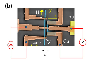
Ultrathin EuS films were deposited by e-beam evaporation with slow growth rate 0.13 /s under a base pressure of 2 10-8 torr. Magnetic property of EuS thin films in the thickness range 2-10 nm were characterized with Quantum Design MPMS magnetometer. Lateral spin valves were fabricated by multi-step e-beam lithography and lift-off process. First 30 nm thick two Permalloy (Ni80Fe20) electrodes were deposited followed by 3 nm MgO in-situ by e-beam evaporation. Then 100 nm thick Cu spin transport channel was deposited in another UHV chamber by a Joule heating evaporator using 99.9999 purity Cu source. Prior to Cu deposition samples were Ar+-ion milled for 40 sec to remove resist left-over. After Cu deposition devices were transferred to another UHV chamber and 5 nm EuS capping layer was deposited following 40 sec in-situ Ar+-ion milling. After Cu lift-off the EuS capped samples were further capped with 2 nm AlOx by rf-sputtering to protect it against oxidation. EuS capped sample without subsequent AlOx capping showed rapid degradation with time. In all other spin valve devices AlOx or MgO capping was done ex-situ after Cu lift-off without any Ar+-ion cleaning process. Therefore presence of native oxide layer on Cu nanowire cannot be ruled out. Another series of lateral spin valves were also fabricated on Si/SiO2/EuS(10 nm) thin film (labeled as EuS substrate) and 2 micrometer YIG film grown on gadolinium gallium garnet (GGG) substrate (labeled as YIG substrate) following similar procedure and capped with AlOx at the end. The YIG thin film grown on GGG substrate was obtained from Innovent e. V. (Jena, Germany). A typical lateral spin valve device with nonlocal measurement configuration is shown in Fig. 1(b). To have different switching fields in two Py nanowires ends of the first Py wire are connected to two large pads which enable the nucleation of domain wall at lower magnetic fields than the thin long Py nanowire. The nonlocal measurements were performed in a continuous flow cryostat using a phase sensitive lock-in technique (modulation frequency = 173 Hz). All the temperature dependent measurements were done in a single heating cycle from 2 to 300 K. For accurate calculation of resistivity dimensions of Cu and Py electrodes were measured by Scanning Electron Microscope (SEM) for each device.
 |
 |
 |
 |
III Results
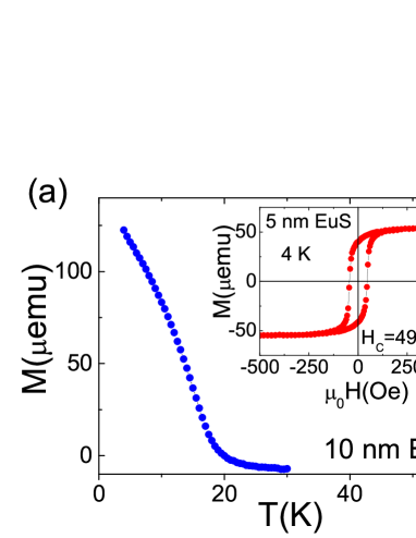
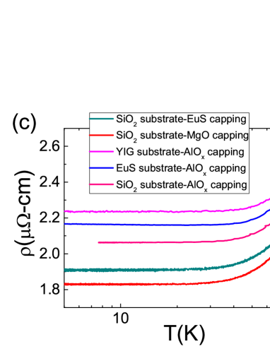
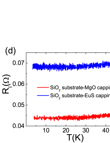
Fig. 1(a) shows temperature dependence of magnetization of a 10 nm thick EuS film deposited by e-beam evaporation. Bulk EuS is known to be an ideal Heisenberg ferromagnetic semiconductor with Curie temperature () of about 16.6 K and band gap of 1.65 eV at room temperaturezinn . A broad ferromagnetic transition with Curie temperature TC 15 K can be seen in Fig. 1(a). This is comparable to values reported for EuS thin films by different groupsmoodera ; Idzuchi-EuS ; wolf . Inset shows magnetization (M-H) loop of a 5 nm thick EuS film measured at 4 K with the magnetic field applied in the film plane. A small coercive field 49 Oe with an almost rectangular loop was found supporting the ferromagnetic properties of the EuS film. We found EuS thin films are magnetic even down to 2 nm. Films were also found to be very smooth with rms roughness 0.54 nm over an area of 1m 1m. The resistivity of EuS films were found to be 0.5 -cm at room temperature. Fig. 1(c) shows temperature dependence of resistivity of Cu spin transport channel in the temperature range 4-200 K with different substrate and capping. The resistivity of Cu nanowire was measured using a 4-point configuration in which current is sent through the Py electrodes and voltage is measured along Cu channel. Temperature axis is plotted in log-scale to identify resistivity minimum considered as an evidence of Kondo effect. No resistivity minimum was observed indicating negligible role of Kondo effect and magnetic impurities. Temperature independent residual resistivity suggest electrical transport in these Cu nanowires arise primarily from scattering with defects, grain boundaries and surface. In these lateral spin valve devices 3 nm MgO layer was inserted between Py and Cu to increase spin injection efficiency. This rules out possibility of ferromagnetic species diffusing into the Cu nanowire which creates magnetic scattering sites. In addition, Py and Cu were deposited in two separate UHV chambers which limit possible interdiffusion of magnetic elements at the interface. Fig. 1(d) shows temperature dependence of Cu/MgO/Py interface resistance for LSVs with MgO and EuS capping. No resistivity upturn was observed suggesting limited interfacial interdiffusion. We found LSV devices fabricated following similar process with no MgO tunnel barrier also showed similar temperature dependence as in Fig. 1(b) (see Supplementary SFig. 1supp ).
 |
 |
 |
 |
 |
 |
 |
 |
In order to create pure spin current in the spin transport channel nonlocal configuration was used as shown in Fig. 1(b). When a spin-polarized current is injected from the Py to Cu electrode through a MgO tunnel barrier, a spin accumulation is built at the interface between the Cu channel and the Py. This induced spin accumulation at Py-MgO-Cu interface is expressed as, , with electrochemical potentials and for up and down spin electrons, respectively. This spin accumulation diffuses away from the interface, creating a pure spin current in the Cu nanowire which is detected as a voltage by the second Py electrode. The nonlocal resistance is defined from the normalization of the detected voltage to the injected current as, . The value of changes sign when the relative magnetization of the Py electrodes is switched from parallel to antiparallel while sweeping applied magnetic field along the long axis of Py. The change from positive to negative is defined as the spin signal, , which is proportional to the spin accumulation at the detector. Therefore magnitude of the spin signal is a measure of total spin relaxation time inside the spin transport channel.
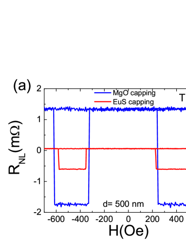
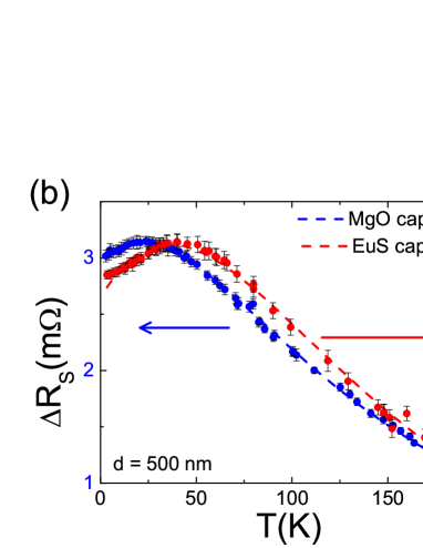
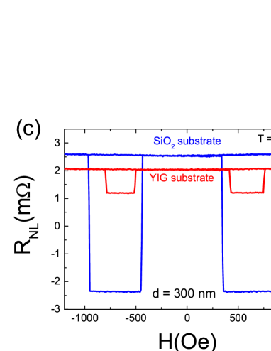
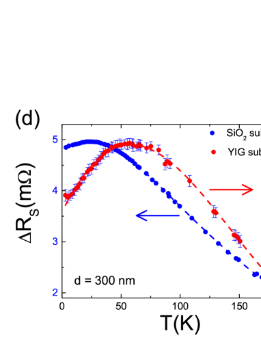
Fig. 2(a) compares spin signal for two LSVs fabricated on Si/SiO2 substrate with EuS and MgO capping layer and same electrode spacing =500 nm. Nonmagnetic MgO capping layer could largely reduce the surface scattering providing ideal reference devices for comparison with EuS capped devicesizuchi . The nonlocal spin valve signal was measured at 5 K below TCurie 15 K of EuS. The spin signal 0.67 m was observed for EuS capped devices which is 4.5 times less than spin signal 3.06 m with MgO capping. A clear suppression of the nonlocal spin valve signal can be observed. The amplitude of the spin signal also depends on thickness of the tunnel barrier and therefore on the Cu/MgO/Py interface resistancefukuma . We found almost similar areal interface resistance = 1.9 and = 0.6 for the EuS and MgO capped device at 10 K(Fig. 1(d)). These areal resistance values are slightly higher than (0.3 ) for spin valve devices with no MgO tunnel barrier and correspond to a semi-transparent tunnel barrierfukuma ; lwang . Fig. 2(c) shows similar nonlocal resistance measurements to the one shown in Fig. 2(a) comparing spin valves fabricated on YIG and SiO2 substrate. For both devices, the same AlOx capping and distance between two Py electrodes = 300 nm were used. The spin signal for the spin valve on YIG substrate was found to be 6 times smaller compared to the reference device fabricated on a non-magnetic SiO2 substrate. Similar suppression of the spin signal on YIG substrates has been observed by other research groups as wellDejene . Fig. 2(b) and (d) shows temperature dependence of spin signal for the same non-local spin valves shown in Fig. 2(a) and (c), respectively. A uniform suppression of the spin signal can be observed at all the temperatures. Furthermore all devices exhibit a clear non-monotonous temperature-dependent behavior, with a peak of the spin signal at low temperatures. In both the reference spin valves either with MgO or AlOx capping the peak in the spin signal was observed around 22 K. This low-temperature peak shifts to higher temperatures if the spin-transport channel is in contact with either EuS ( = 40 K) or YIG ( = 60 K). As both EuS and YIG are insulators no charge current will flow through them. We believe this peak shift originates from interfacial effects as will be discussed later on.
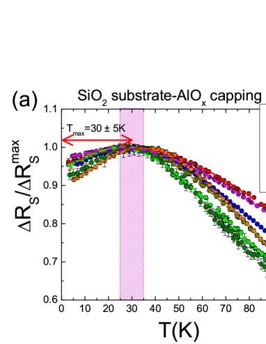
We further investigated the peak shift of the spin signal by comparative temperature dependent measurements on lateral spin valves with varying injector - detector distance . Fig. 3(a) shows temperature dependence of spin signal normalized to their maximum value for several lateral spin valves on Si/SiO2 substrate and AlOx capping. Irrespective of injector to detector distance low temperature peak can be seen to appear at T =30 5 K. Also spin signal drops only 10 from the maximum value at low temperature. The relationship between the injector-detector distance and the spin signal can be described by a scaling lawsupp ;
| (1) |
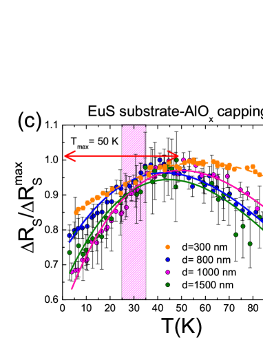
where is the injector-detector spacing and is a multiplication factor. This scaling law suggest that irrespective of the reduction of the magnitude of spin signal with increased electrode spacing by , temperature dependence of spin signal for all the spacing can be superimposed onto each other with a constant multiplication factor . Fig. 3(b) shows temperature-dependent spin signal measurements on EuS capped LSV devices with varying injector-detector distance . Here a wide dispersion of the temperatures corresponding to the peak maximum can be observed. In particular, for the LSV device with =300 nm the peak position is as high as 50 K. Besides relative drop of the spin signal is quite high 25 from its maximum value. It is obvious, that the curves in Fig. 3(b) cannot be superimposed using Eq. (1), and the deviation from this scaling suggest that additional temperature-dependent spin sinking effects are present in the EuS capped LSV devices.
To further understand the anomalous low temperature behavior in the nonlocal spin valves in contact with EuS, we investigated another set of LSVs fabricated on Si/SiO2/EuS(10 nm) thin film and capped with AlOx. In this set of samples, the spin-transport channel might be in more uniform contact with the smooth EuS film, as compared to the EuS-capped devices, which might have non-uniform coverage. Fig. 3(c) shows normalized temperature dependent spin signal of devices fabricated on EuS substrate for different . The peak positions are found at temperatures T 50 K and a huge drop of the spin signal up to 30 compared to maximum value can be seen at low temperatures. In comparison with EuS capped LSV devices, the devices grown on top of a EuS substrate show no significant dependence in the low temperature regime. A possible explanation for the observed peak shifts to higher temperatures might originate from effects like spin back flow into Py and anisotropic spin absorption at the Py/Cu interfaces particularly when injector - detector distance is comparable or shorter than spin diffusion length of CuObrien-prb ; izuchi-prb ; izuchi-rev . We believe the anomalous low temperature behavior observed in our case does not originate from these effects, as the shift would show a pronounced dependence of the injector-detector distance .
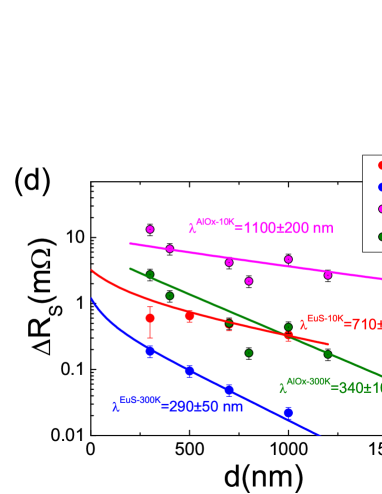
The variation of the spin signal amplitudes for devices having different injector-detector gaps summarized for EuS and AlOx-capped devices is shown in Fig. 3(d). Based on the one-dimensional spin diffusion model spin signal for a in-plane magnetic field can be written asTakahashi ;
| (2) |
where , , and are the spin resistances of Cu, Py and MgO interface, respectively. Here is the resistivity, is the spin polarization, is spin diffusion length, is thickness, and is the width of wire (= Cu, Py or MgO). Here stands for Py/MgO/Cu areal interface resistance which was measured separately for each devices and an average = 1.9 and = 27.9 was used for fitting purposes. Furthermore, the following values for Py at 10 K (300 K) were assumedSagasta : =32 -cm(44 -cm), = 3 nm(2.3 nm), and = 0.39 (0.31). Fitting the data points shown in Fig. 3(d) to Eq. (2) we extracted spin diffusion length of Cu at 10 K (300 K) on SiO2 substrate with AlOx capping as 1100200 nm (340 100 nm). These values are in good agreement with reported values for Cu/Py lateral spin valvesJedema ; villamor-nlsv ; taro . A set of device properties obtained from experiments and fitting Eq. (2) is summarized in Table 1. From the spin diffusion length the spin relaxation time can be calculated via, , where is the diffusion constant. The diffusion constant was calculated from Einstein relation, with the resistivity and (=1.8 states/eVm3Jedema ) is the density of state at Fermi energy of Cu. The momentum relaxation time due to defects was calculated using . Here (= m/s) is the Fermi velocity of CuJedema .
| LSV | (-cm) | (nm) | (fs) | (ps) | () | () | ||||||
|---|---|---|---|---|---|---|---|---|---|---|---|---|
| AlOx capping | 2.06 | 1100200 | 20.5 | 71.8 | 0.285 | 2.85 | ||||||
| EuS capping | 1.91 | 710100 | 22.1 | 27.7 | 0.799 | 7.98 |
The spin-flip probability at the surface can be defined as, , where = / denotes the interfacial spin-flip parameterbass . From the values given in Table. 1, it is obvious that EuS capped spin valves have higher spin flip probability compared to AlOx capping. We believe this enhanced spin-flip probability in the EuS capped LSV devices originates from spin-flip scattering caused by the spin-orbit and exchange fields at the Cu-EuS interface. Due to due to high atomic number of Eu ( = 63) the spin-orbit field at the Cu-EuS interface is larger than at Cu-AlOx interface ( = 13). The suppression of spin signal in EuS capped devices as compared to the reference devices in full temperature range therefore point to the spin-orbit field as the major cause of spin signal suppression. However, anomalous scaling of the spin signal with the injector-detector distance in the EuS capped LSV devices cannot be explained with only spin-orbit fields. Therefore, in order to explain total drop in the spin signal one must also consider spin relaxation caused by interfacial exchange field and spin sinking due to thermal magnons. Thus the spin diffusion length in these LSV devices can be calculated considering spin-mixing effects at the Cu-EuS interface. Following the approach developed by Dejene et. al.Dejene effective spin-relaxation length () of Cu in the EuS capped devices can be written assupp ,
| (3) |
where is the spin-diffusion length of Cu on SiO2 substrate and denotes a length scale which takes interfacial spin sinking effects into account. From the value of the effective spin-mixing conductance per area can be determined using the equation , with Cu nanowire thickness = 100 nm and the Cu resistivity = 1.91 -cm. We found an effective spin mixing conductance 3.03 1012 for the EuS capped LSV, 1.2 1013 for the LSV on EuS substrate, and 2.67 1013 for LSV on YIG substrates. These values are comparable to spin-mixing conductance 1013 found for Al/YIG interfacesDejene . Therefore, using interface engineering, it might be possible to improve values of for Cu-EuS interface leading to an effective spin current gating for spintronic devices.
IV Discussion
One of the main findings of our work is the observation of a low-temperature peak in the spin signal of all fabricated non-local spin valves, and furthermore the subsequent shift of the peak to higher temperatures for devices in contact with a magnetic insulator substrate or capping layer. The low-temperature peak in the spin signal of lateral spin valves fabricated from high-purity Cu has been observed by many research groups, but its physical origin is still under debate, as its existence is not described by the EY-mechanism used to explain spin relaxation in lateral spin valve devices Elliott ; Yafet . Within the framework of the EY-mechanism, the spin diffusion length is predicted to increase monotonically with decreasing temperature. This prediction stands in contrast to experimental observations where the spin signal of lateral spin valves is usually found to decrease below 30 K, even though the Cu resistivity, and thus the momentum relaxation time, remain constant at low temperature (as demonstrated in Fig. 1(c)). To explain the peak in the spin signal around 30 K, different mechanism including surface scattering Erekhinsky ; Kimura ; villamor-nlsv ; mihajlovic , magnetic impurities in bulk Cu or the vicinity of the Py/Cu interfacezhou ; obrien ; batley ; watts ; hamaya ; Villamor-prb-nlsv ; kim , or changes in spin polarization of Cu/Py interfaceObrien-natcomm have been proposed. The existence of a small fraction (parts per million) of magnetic impurities in bulk Cu is believed to cause spin-flip scattering associated with the Kondo effect, which leads to a suppression of the spin-diffusion length at low temperatures. This effect has been extensively investigated using different magnetic impurities inside a host nonmagnetic metalhamaya ; obrien ; batley . One of the observations from these experiments is that peak in the spin signal appears at much higher temperature than the Kondo temperature ()Obrien-natcomm ; batley ; hamaya . Alternatively, surface spin-flip scattering has been shown to contribute to an anomalous drop of the spin signal at low temperaturesKimura ; villamor-nlsv . Interestingly, experimental results indicate that the surface spin-flip rate increases with the atomic number of the atomic species at the surface, suggesting that the spin-orbit field at the surface plays a crucial role in the spin relaxationkarube . In the pioneering work of Fert et. al.fert , it was demonstrated that the spin relaxation due to spin-orbit scattering is temperature-independent, in contrast to the temperature-dependent exchange scattering. The fingerprints of spin relaxation due to the interfacial exchange field can be seen only at low temperature, where other temperature-dependent spin relaxation processes are less prominent. Therefore, temperature-dependent spin transport measurements on LSV devices provide an unique way to extract information about the intrinsic interfacial exchange field present at the FI/NM interface.
Recently, spin transport behavior of LSV in contact with a ferromagnetic insulator has been theoretically modeledVillamor-yig ; Dejene . When LSV is in proximity with a ferromagnetic insulator spin angular momentum transfer occurs at the interface and one has to consider additional boundary condition for spin current density, which can be expressed asDejene ; supp ; Matthias
| (4) |
Here is the unit vector parallel to in-plane magnetization of EuS or YIG, and are real and imaginary part of spin-mixing conductance per unit area, and is additional spin sinking term independent of magnetization direction. According to this boundary condition when the spin polarization of spin current in the metallic channel is perpendicular to the magnetization, spin angular momentum can be transferred to the magnetization of FI through spin transfer torques. On the contrary when the polarization of the spin current is aligned along the magnetization, the spin current cannot penetrate into the insulator and is reflected back into the NM. Successful observation of spin current modulation in LSVs on YIG substrate has been attributed to a larger value of the real part of spin mixing conductance at the NM/YIG interfaceVillamor-yig ; Dejene . However, in these experiments role of interfacial exchange field were not addressed. One can notice that in our measurements magnetization of EuS and both injector-detector Py are all collinear, therefore, observed spin memory loss cannot be explained by spin transfer torque. In collinear case only the effective spin sink conductance becomes relevant. Temperature dependence of spin signal can be explained considering temperature dependence of Matthias . However, the effective spin sink conductance is not clearly defined near and above the Curie temperatureCornelissen . Therefore, model based on Eq. (7) may not be sufficient to explain temperature dependent spin signal of LSVs in contact with EuS.
Recently, anomalous temperature dependent spin signal was also observed in graphene spin valves in contact with YIGSimranjeet . Alternative approach was developed considering randomly fluctuating exchange fields. In our experiments anomalous low temperature behavior most likely appears due to spin relaxation caused by interfacial exchange field at the Cu-EuS (or Cu-YIG) interface. At finite temperatures, the Eu moments (Fe-moment in case of YIG) fluctuate around the local equilibrium state producing fluctuating exchange field () at the interface. Although the Curie temperature of EuS is 15 K thermal fluctuation of Eu moments can survive at temperatures above as seen in some ferromagnetsQin . These fluctuating exchange field exponentially decay with time as, , where is the fluctuation correlation time. According to Matthiessen’s rule total spin-flip time after considering contribution from fluctating exchange field can be written as,
| (5) |
Here , and represents spin-flip scattering time due to non-magnetic impurities or defects, phonons and interfacial exchange field, respectively. According to Elliott-Yafet theory spin relaxation () from nonmagnetic defects are temperature independentElliott ; Yafet . Also at low temperature phonon contribution to the spin relaxation rate vanishes. This leaves the fluctuating exchange field as the only temperature-dependent contribution to the spin relaxation. Based on the exchange-field model developed by McCreary et. al.McCreary , the spin-relaxation rate due to the fluctuating exchange field can be written as,
| (6) |
where is the rms value of exchange field fluctuation amplitude in the transverse direction, is applied magnetic field, is the magnitude of exchange field and is the fluctuation correlation time. The spin-relaxation rate in Eq. [6] is temperature dependent as interfacial exchange field which is determined by magnetization is temperature dependent. Recent measurements of our group on metallic spin glass like CuMnBi further showed that the spin Hall angle decreases at temperatures well above the materials spin-glass temperature nimmi-jpsj . This unusual temperature dependence has been understood considering magnetic fluctuations of Mn moment which can be detected more sensitively by spin Hall effectziman . All these experiment suggest temperature dependent measurement involving spin current can be used to study fluctuating interfacial exchange field in a more precise manner than charge transport methods.
V Conclusions
In summary, we presented a detailed study of temperature-dependent spin signal of non-local spin valves in contact with magnetic EuS or YIG, and compared these to reference devices adjacent to nonmagnetic MgO or AlOx. We found that the spin signal is suppressed for devices in contact with a magnetic EuS or YIG layer, and attribute this suppressed signal to an enhanced surface scattering originating from the spin-orbit fields at the interface to the magnetic capping layer or substrate. Besides spin signal suppression we found widely observed low temperature peak in the spin signal was shifted to much higher temperature compared to control LSV devices. Furthermore, the spin signal was found to scale in an anomalous way with the injector-detector distance of these LSV devices. We believe these additional temperature dependent spin sinking effects arise due to fluctuating exchange field at the Cu-EuS or Cu-YIG interfaces. The strength of this exchange field can be determined in the future using Hanle spin-precession experiments. Moreover anomalous temperature dependence observed in our spin valve devices provide an unambiguous evidence for the presence of exchange field at the EuS-Cu interface. With careful engineering of the interface quality it might be possible to demonstrate magnetically controlled modulation of the spin current in these devices. The ongoing development and miniaturization in the field of spintronics demands ultrathin magnetic films which are stable under ambient conditions and easy integrability into nanoscale metallic devices. Our experimental results suggest ferromagnetic insulator EuS can be a handy material for nanoscale spintronics devices.
Acknowledgments
This work was supported by a Grant-in-Aid for Scientific Research
on Innovative Area, Nano Spin Conversion Science (Grant No.
26103002). SPD thanks Swedish Research Council project grant (No.
2016-03658). We would like to thank Dr T. Nakamura and Prof S.
Katsumoto for the use of the lithography facilities. We also thank
Dr Naëmi Riccarda Leo for proofreading the manuscript.
References
- (1) Y. Otani, M. Shiraishi, A. Oiwa, E. Saitoh and S. Murakami, Nature Physics 13, 829 (2017).
- (2) A. Soumyanarayanan, N. Reyren, A. Fert, C. Panagopoulos, Nature 539, 509 (2016).
- (3) F. Hellman, A. Hoffmann, Y. Tserkovnyak, G. S. Beach, E. E. Fullerton, C. Leighton, A. H. MacDonald, D. C. Ralph, D. A. Arena, H. A. D rr, P. Fischer, J. Grollier, J. P. Heremans, T. Jungwirth, A. V. Kimel, B. Koopmans, I. N. Krivorotov, S. J. May, A. K. Petford-Long, J. M. Rondinelli, N. Samarth, I. K. Schuller, A. N. Slavin, M. D. Stiles, O. Tchernyshyov, A. Thiaville, and B. L. Zink, Rev. Mod. Phys. 89, 025006 (2017).
- (4) V. M. Edelstein, Solid State Commun. 73, 233 (1990).
- (5) J. C. Rojas S nchez, L. Vila, G. Desfonds, S. Gambarelli, J. P. Attan , J. M. De Teresa, C. Mag n and A. Fert, Nature Communications 4, 2944 (2013).
- (6) Y. Tserkovnyak, A. Brataas, G. E. W. Bauer, and B. I. Halperin, Rev. Mod. Phys. 77, 1375 (2005).
- (7) D. C. Ralph and M. D. Stiles, J. Magn. Magn. Mater. 320, 1190 (2008).
- (8) K. Uchida, J. Xiao, H. Adachi, J. Ohe, S. Takahashi, J. Ieda, T. Ota, Y. Kajiwara, H. Umezawa, H. Kawai, G. E. W. Bauer, S. Maekawa, and E. Saitoh, Nat. Mater. 9, 894 (2010).
- (9) J. Flipse, F. K. Dejene, D. Wagenaar, G. E. W. Bauer, J. Ben Youssef, and B. J. van Wees, Phys. Rev. Lett. 113, 027601 (2014).
- (10) H. Nakayama, M. Althammer, Y.-T. Chen, K. Uchida, Y. Kajiwara, D. Kikuchi, T. Ohtani, S. Gepr gs, M. Opel, S. Takahashi, R. Gross, G. E. W. Bauer, S. T. B. Goennenwein, and E. Saitoh, Physical Review Letters 110, 206601 (2013).
- (11) S. T. B. Goennenwein, R. Schlitz, M. Pernpeintner, K. Ganzhorn, M. Althammer, R. Gross, and H. Huebl, Appl. Phys. Lett. 107, 172405 (2015).
- (12) R. J. Elliott, Phys. Rev. 96, 266 (1954).
- (13) Y. Yafet, Solid State Phys. 14, 1 (1963).
- (14) E. Villamor, M. Isasa, S. V lez, A. Bedoya-Pinto, P. Vavassori, L. E. Hueso, F. S. Bergeret, and F. Casanova, Phys. Rev. B 91, 020403 (2015).
- (15) F. K. Dejene, N. Vlietstra, D. Luc, X. Waintal, J. Ben Youssef, and B. J. van Wees, Phys. Rev. B 91, 100404(R)(2015).
- (16) S. Maekawa, H. A. Adachi, K. Uchida, J. Ieda, and E. Saitoh, J. Phys. Soc. Jpn. 82, 102002 (2013).
- (17) G.X. Miao, J.S. Moodera, Phys. Chem. Chem. Phys. 17, 751 (2015).
- (18) E. Strambini, V. N. Golovach, G. De Simoni, J. S. Moodera, F. S. Bergeret, and F. Giazotto,Phys. Rev. Materials 1, 054402 (2017).
- (19) J. S. Moodera, T. S. Santos, and T. Nagahama, J. Phys.: Condens. Matter 19, 165202 (2007).
- (20) X.Hao, J.S.Moodera, and R. Meservey, Phys. Rev. B 42,8235 (1990).
- (21) P. Wei, F. Katmis, B. A. Assaf, H. Steinberg, P. Jarillo-Herrero, D. Heiman, and J. S. Moodera, Phys. Rev. Lett. 110, 186807 (2013).
- (22) P. Wei, S. Lee, F. Lemaitre, L. Pinel, D. Cutaia, W. Cha, F. Katmis, Y. Zhu, D. Heiman, J. Hone, J. S. Moodera, and C.-T. Chen, Nat. Mater. 15, 711 (2016).
- (23) C. Zhao, T. Norden, P. Zhang, P. Zhao, Y. Cheng, F. Sun, J. P. Parry, P. Taheri, J. Wang, Y. Yang, T. Scrace, K. Kang, S. Yang, G.-x. Miao, R. Sabirianov, G. Kioseoglou, W. Huang, A. Petrou, and H. Zeng, Nat. Nanotechnol. 12, 757 (2017).
- (24) F. Katmis, V. Lauter, F. S. Nogueira, B. A. Assaf, M. E. Jamer, P. Wei, B. Satpati, J. W. Freeland, I. Eremin, D. Heiman, P. Jarillo-Herrero, and J. S. Moodera, Nature (London) 533, 513 (2016).
- (25) C. Leutenantsmeyer, A. A. Kaverzin, M. Wojtaszek, and B. J. van Wees, 2D Materials 4, 014001 (2017).
- (26) W. Zinn, J. Magn. Magn. Mater.3, 23(1976).
- (27) H. Idzuchi, Y. Fukuma, H. S. Park, T. Matsuda, T. Tanigaki, S. Aizawa, M. Shirai, D. Shindo, and Y. Otani, Appl. Phys. Exp. 7, 113002 (2014).
- (28) M. J. Wolf, C. Surgers, G. Fischer, T. Scherer, D. Beckmann, J.Magn. Magn. Mater. 368,499 (2014).
- (29) See Supplemental Material at http://link.aps.org/ supplemental/ for LSV with no MgO tunnel barrier, Energy-dispersive X-ray(EDX) spectra to validate presence of EuS on the EuS capped device, Note on scaling Eq. [1], and Calculation of effective spin relaxation length of Cu in LSV in contact with FI (EuS or YIG).
- (30) H. Idzuchi, Y. Fukuma, L. Wang, and Y. Otani, Appl. Phys. Lett. 101, 022415 (2012).
- (31) Y. Fukuma, L. Wang, H. Idzuchi, S. Takahashi, S. Maekawa, and Y. Otani, Nature Materials 10, 527 (2011).
- (32) L. Wang, Y. Fukuma, H. Idzuchi, and Y. Otani, J. Appl. Phys. 109, 07C506 (2011).
- (33) L. O Brien, D. Spivak, N. Krueger, T. A. Peterson, M. J. Erickson, B. Bolon, C. C. Geppert, C. Leighton, and P. A. Crowell, Phys. Rev. B 94, 094431 (2016).
- (34) H. Idzuchi, Y. Fukuma, S. Takahashi, S. Maekawa, and Y. Otani Phys. Rev. B 89, 081308(R) (2014).
- (35) H. Idzuchi, Y. Fukuma, Y. Otani, Physica E 68, 239 (2015).
- (36) S. Takahashi and S. Maekawa, Sci. Technol. Adv. Mater.9, 014105 (2008).
- (37) E. Sagasta, Y. Omori, M. Isasa, Y. Otani, L. E. Hueso, and F. Casanova, Appl. Phys. Lett. 111, 082407 (2017).
- (38) F. J. Jedema, M. S. Nijboer, A. T. Filip, and B. J. van Wees, Phys. Rev. B 67, 085319 (2003).
- (39) E. Villamor, M. Isasa, L. E. Hueso, and F. Casanova, Phys. Rev. B 87, 094417 (2013).
- (40) T. Wakamura, K. Ohnishi, Y. Niimi, and Y. Otani, Applied Physics Express 4, 063002(2011).
- (41) J. Bass and W. P. Pratt Jr., J. Phys. Condens. Matter 19, 183201 (2007).
- (42) M. Erekhinsky, A. Sharoni, F. Casanova, and I. K. Schuller, Appl. Phys. Lett. 96, 022513 (2010).
- (43) T. Kimura, T. Sato, and Y. Otani,Phys. Rev. Lett. 100, 066602 (2008).
- (44) G. Mihajlovic, J. E. Pearson, S. D. Bader, and A. Hoffmann, Phys. Rev. Lett. 104, 237202 (2010).
- (45) H. Zhou and Y. Ji, Appl. Phys. Lett. 101, 082401 (2012).
- (46) L. ÓBrien, D. Spivak, J. S. Jeong, K. A. Mkhoyan, P. A. Crowell, and C. Leighton, Phys. Rev. B 93, 014413 (2016).
- (47) J. T. Batley, M. C. Rosamond, M. Ali, E. H. Linfield, G. Burnell, and B. J. Hickey, Phys. Rev. B 92, 220420(R) (2015).
- (48) J. D. Watts, J. S. Jeong, L. O fBrien, K. A. Mkhoyan, P. A. Crowell, and C. Leighton, Appl. Phys. Lett. 110, 222407 (2017).
- (49) K. Hamaya, T. Kurokawa, S. Oki, S. Yamada, T. Kanashima, and T. Taniyama, Phys. Rev. B 94, 140401(R) (2016).
- (50) E. Villamor, M. Isasa, L. E. Hueso, and F. Casanova, Phys. Rev. B 88, 184411 (2013).
- (51) K.-W. Kim, L. O’Brien, P. A. Crowell, C. Leighton, and M. D. Stiles, Phys. Rev. B 95, 104404 (2017).
- (52) L. O Brien, M. J. Erickson, D. Spivak, H. Ambaye, R. J. Goyette, V. Lauter, P. A. Crowell, and C. Leighton, Nat. Commun. 5, 3927 (2014).
- (53) S. Karube, H. Idzuchi, K. Kondou, Y. Fukuma, and Y. Otani, Appl. Phys. Lett. 107, 122406 (2015).
- (54) A. Fert, J.-L. Duvail, and T. Valet, Phys. Rev. B 52, 6513 (1995).
- (55) Matthias Althammer, arXiv:1802.08479
- (56) L. J. Cornelissen, K. J. H. Peters, G. E. W. Bauer, R. A. Duine, and B. J. van Wees, Phys. Rev. B 94, 014412 (2016).
- (57) S. Singh, J. Katoch, T. Zhu, K.-Y. Meng, T. Liu, J. T. Brangham, F. Yang, M. E. Flatt , and R. K. Kawakami, Phys. Rev. Lett. 118, 187201 (2017).
- (58) H. J. Qin, Kh. Zakeri, A. Ernst, and J. Kirschner, Phys. Rev. Lett. 118, 127203 (2017).
- (59) K. M. McCreary, A. G. Swartz, W. Han, J. Fabian, and R. K. Kawakami, Phys. Rev. Lett. 109, 186604 (2012).
- (60) Y. Niimi, D. Wei, and Y. Otani, J. Phys. Soc. Jpn. 86, 011004 (2017).
- (61) T. Ziman, B. Gu, and S. Maekawa, J. Phys. Soc. Jpn. 86, 011005 (2017).