Quantum transport by spin-polarized edge states in graphene nanoribbons in the quantum spin Hall and quantum anomalous Hall regimes
Abstract
Using the non-equilibrium Green’s function method and the Keldysh formalism, we study the effects of spin-orbit interactions and time-reversal symmetry breaking exchange fields on non-equilibrium quantum transport in graphene armchair nanoribbons. We identify signatures of the quantum spin Hall (QSH) and the quantum anomalous Hall (QAH) phases in non-equilibrium edge transport by calculating the spin-resolved real space charge density and local currents at the nanoribbon edges. We find that the QSH phase, which is realized in a system with intrinsic spin-orbit coupling, is characterized by chiral counter-propagating local spin currents summing up to a net charge flow with opposite spin polarization at the edges. In the QAH phase, emerging in the presence of Rashba spin-orbit coupling and a ferromagnetic exchange field, two chiral edge channels with opposite spins propagate in the same direction at each edge, generating an unpolarized charge current and a quantized Hall conductance . Increasing the intrinsic spin-orbit coupling causes a transition from the QAH to the QSH phase, evinced by characteristic changes in the non-equilibrium edge transport. In contrast, an antiferromagnetic exchange field can coexist with a QSH phase, but can never induce a QAH phase due to a symmetry that combines time-reversal and sublattice translational symmetry.
pacs:
73.21.HB, 85.75.Hh.I INTRODUCTION
Two-dimensional (2D) topological insulators (TIs) in the presence of time-reversal symmetry (TRS) can display the quantum spin Hall (QSH) effect, and therefore are also known as QSH insulators Qi and Zhang (2010). In the QSH state the electronic system is characterized by a non-trivial topological bulk gap, opened by spin-orbit interaction (SOI), separating the valence and conduction bands. In a Hall bar geometry, a QSH insulator hosts at each edge a pair of gapless one-dimensional (1D) channels, with opposite spin and moving in opposite directions, whose linear dispersions cross inside the bulk gap. The charge current carried by these edge states is dissipationless in the absence of magnetic scattering, and the longitudinal conductance is quantized in units of . At the same time a QSH state displays spin accumulation at the edges, leading to a spin Hall resistance, which typically is not quantized, since in general spin is not conserved.
The first theoretical prediction of the QSH effect was made by Kane and Mele in 2005 (Kane and Mele, 2005a, b) on the basis of 2D models describing graphene nanoribbons. In bulk graphene, the conduction and valence bands meet at two inequivalent Dirac points (DPs). Intrinsic SOI opens a small topological gap at these DPs, inside which 1D edge states can appear, causing the QSH effect. Since the intrinsic SOI in pure graphene is very weak, the resulting gap is too small for the QSH effect to be observed (the SOI induced gap is estimated to be a fraction of meV in graphene Min et al. (2006); Boettger and Trickey (2007)). On the other hand, the QSH effect has been verified experimentally in mercury tellurride (HgTe) quantum wells, another 2D TI König et al. (2007). Nevertheless, since graphene is such a remarkable opto-electronic 2D material, intensive efforts to realize experimentally the QSH state have continued in recent years, focusing on the artificial enhancement of the intrinsic SOI, e.g. by embedding heavy atoms into the graphene lattice Klimovskikh et al. (2017).
From a fundamental point of view, graphene is the ideal model system to investigate the fate of the QSH effect in 2D TIs when TRS is broken, e.g. by the proximity of a magnetic substrate inducing an exchange interaction on the graphene electrons. A theoretical study Yang et al. (2011) based on the Kane and Mele graphene model in the presence of Rashba SOI and a ferromagnetic (FM) exchange field shows that the exchange interaction can drive the system from the QSH regime into a new topological phase known as the quantum anomalous Hall (QAH) regime. Like the ordinary quantum Hall effect, the QAH effect refers to the quantization of the Hall conductance in a 2D electron system where TRS is broken. In contrast to the quantum Hall effect, the QAH effect occurs in the absence of an external magnetic field. The possibility of this effect was first proposed by Haldane based on studies of a tight-binding toy model on the same honeycomb lattice in the presence of a periodic magnetic field with zero net flux Haldane (1988).
In Ref. Yang et al., 2011 and in other theoretical work based either on similar lattice models (Qiao et al., 2010) or on ab initio studies of a graphene sheet on magnetic insulator substrates (Qiao et al., 2014), the emergence of the QAH effect in graphene is typically established by computing the Berry curvature and the Chern number for the valence bands of the 2D bulk system. A non-zero Chern number corresponds to a quantized Hall conductance.
The purpose of the present paper is to investigate the effect of TRS-breaking exchange fields on the QSH phase in graphene directly from the point of view of out-of-equilibrium quantum transport in a nanoribbon. Specifically, we carry out a computational study of the non-equilibrium spin-polarized charge density and local current at the edges of an armchair graphene nanoribbon, which characterize the 1D conducting states responsible for both the QSH and the QAH effect. Typically, transport properties are experimentally determined via conductance measurements obtained using four-probe techniques. However, the spatial details of the current can be measured using scanning probe microscopy Topinka et al. (2003), optical Kerr rotation microscopy Crooker et al. (2005), or indirectly by nuclear magnetic resonance techniques Walz et al. (2014). A FM exchange field drives the system into a QAH phase when only a Rashba SOI is present. However, when both Rashba and intrinsic SOI are present, we show that there is a regime, controlled by their relative strength, where the QSH phase survives even in the presence of the FM exchange field. In contrast, an antiferromagnetic (AFM) exchange field can never induce a transition from a QSH to a QAH phase, due to a combination of TRS and sublattice translational symmetry.
The paper is organized as follows. In Sec. II, we introduce the tight-binding model and the formalism for quantum transport in graphene nanoribbons. In particular, the calculation of non-equilibrium spin-polarized density and the local current is discussed. The results of our calculations are presented in Sec. III. In Sec. III.1, we describe spin-polarized transport in the QSH regime. The effect of an exchange field on transport and the transition to the QAH state are studied in Sec. III.2.
II MODEL AND METHOD
In order to calculate transport properties of a graphene nanoribbon, we use the non-equilibrium Green’s function (NEGF) technique in a two-terminal system consisting of a central channel attached to two semi-infinite leads. The Hamiltonian of the central region can be written in the second quantized form (Konschuh et al., 2010)
| (1) | |||||
Here, is the electron creation (annihilation) operator with spin at site on the honeycomb lattice and is the vector of Pauli matrices. The first term in Eq. 1 is the usual nearest-neighbor (NN) hopping term with eV. The second term represents an exchange field of strength , ferromagnetic when and antiferromagnetic when , with the sign being opposite on the two sublattices. The third term, involving the next nearest-neighbor (NNN) sites and , is the intrinsic SOI with strength . The constant , depending on whether the NNN hopping is clockwise or counter clockwise with respect to the positive axis. Finally, the fourth and last term is a spin-dependent NN hopping representing a Rashba SOI, where is the unit vector in real space connecting site to site .
Here, we will consider values of the SOI parameters that are large enough to produce significant effects. This model is therefore supposed to represent graphene nanoribbons where the SOI has been artificially enhanced, or other 2D atomic monolayers on a honeycomb lattice such as stanene andFeng-feng Zhu et al. (2015); Xiong et al. (2016); Wang et al. (2016), where intrinsic SOI is considerably larger than in graphene and is expected to produce a large-gap 2D QSH effect. Given the Hamiltonian of the central channel, the spin-dependent retarded () and advanced () Green’s functions are given by (Datta, 1997), where and is an identity matrix. In this equation, is the self-energy due to the connection of the left (right) semi-infinite electrode to the central channel. is the surface Green’s function of the left(right) lead; is calculated iteratively by adding one unit cell from the central region at a time using the method of Ref. Lopez Sancho et al., 1984. Therefore, the Green’s functions of a central region consisting of unit cells each containing atoms can be efficiently calculated using matrices, where 2 comes from the spin-degree of freedom. is the tunneling Hamiltonian between the central region and the left(right) lead. The Hamiltonian of the leads, as well as the tunneling Hamiltonian, is identical to that of the central region, namely it is given by Eq. 1, except that it does not include the exchange field. Now that we have the Green’s functions, the conductance can be calculated as , where is the broadening due to the electrode contacts and the trace is taken over the sites in the sub-matrix.
In order to calculate the steady-state local transport properties in the full NEGF formalism, we need both the retarded and lesser Green’s functions, which contain information about the density of available states and how electrons occupy these states, respectively. In the phase-coherent regime where interaction self-energy functionals are zero, by using the Keldysh formalism we can simply write the lesser Green’s function in terms of the retarded Green’s function and the broadening matrices as (Cresti et al., 2003)
| (2) |
Once the lesser Green’s function are known, we calculate the out-of-equilibrium, spin-resolved, local charge density, . Instead of the full non-equilibrium local charge density Mahfouzi and Nikolić (2013), we use the non-equilibrium definition (Nikolić et al., 2006; Zârbo and Nikolić, 2007; Chen et al., 2010)
| (3) |
as this quantity sensitively depends on the contribution from the edge states appearing in the bulk gap and therefore is useful for investigating the QSH and QAH phases in the transport regime.
To address the transport properties of the nanoribbon, it is appropriate to use the notion of bond currents Todorov (2002). This concept arises naturally from the time derivative of the electron number operator at site , . The equation of motion leads to a continuity equation for the charge given by Nikolić et al. (2006), where is the bond charge current operator describing the charge current flowing from site to the neighboring site via a bundle of flow lines connecting the two sites Todorov (2002). The bond charge current can be seen as the sum over spin-resolved bond charge currents, , where the spin-dependent bond charge current operator is
| (4) |
and includes all the hopping parameters connecting the two different sites as specified by the Hamiltonian 1. I.e., incorporates the spin-dependent and spin-independent Rashba NN hopping as well as the NNN hopping. Taking the quantum-statistical average of Eq. 4, the spin-resolved charge current, , can be expressed in terms of non-equilibrium Keldysh Green’s functions Caroli et al. (1971). Neglecting the SOI contributions in because , the NN spin-resolved bond charge current is diagonal in spin space such that , and can be written as Nikolić et al. (2006)
| (5) |
However, note that still depends on the intrinsic and Rashba SOI via the Green’s functions.
III RESULTS AND DISCUSSION
The electronic states of graphene nanoribbons, and therefore their transport properties, strongly depend on their edge structure. There are two different types of graphene nanoribbons, zigzag graphene nanoribbons (ZGNRs) and armchair graphene nanoribbons (AGNRs). In the absence of SOI, ZGNRs are always metallic; AGNRs, which are the ones considered here, can be either metallic or semiconducting depending on their width. An AGNR is metallic for widths such that the number of dimers along the transverse direction in a unit cell consisting of atoms satisfies the relation , with being an integer. (See Fig. 2 for an AGNR with .)
III.1 Intrinsic spin-orbit coupling: the QSH effect
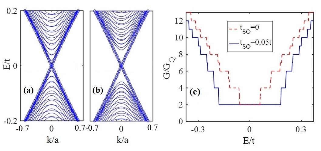
We start with the case where only intrinsic SOI is included in the model, leading to the QSH regime. Figs. 1(a) and (b) show the band structure for an nanoribbon without and with intrinsic SOI, respectively. In both cases two linearly dispersing bands, crossing at at energy , traverse an energy gap separating all other positive- and negative-energy 1D energy subbands with ordinary quadratic dispersion. When the energy gap shrinks with increasing width, and bulk 1D bands start to pile up toward . In contrast, when the gap remains finite and converges to the SOI-induced gap of 2D bulk graphene. This feature of the bandstructure has implications for the transport properties: while in the absence of SOI the energy region where ( being the conductance quantum) vanishes for large-width nanoribbons, in the presence of SOI this region remains finite and is controlled by the SOI strength. The two branches with linear dispersion are spin-degenerate “edge states,” in the sense that they emerge in a graphene system with edges, such as a nanoribbon. However, their nature is quite different, depending on whether SOI is present or not. In the first case, for a given , the two states with opposite spin components are entirely space localized at the opposite edges of the nanoribbon. Therefore, in the presence of SOI, each edge has a right-moving () state of a given spin and a left-moving () state with opposite spin, both of energy . In contrast, when SOI is absent, the two states with the same and opposite spin have the same space wave function, which is distributed throughout the nanoribbon.
These linearly-dispersed edge states completely determine the conductance of the nanoribbon when the Fermi energy is located within the energy gap . As shown in Fig. 1(c), the topologically trivial () and nontrivial () state display the same transport behavior: the total conductance is quantized, i.e. . This result is expected, since in this disorder-free nanoribbon for both cases there are two perfectly conducting edge states.
The onset of the QSH effect in transport becomes evident if we look at the out-of-equilibrium, spin-resolved charge density in a device made by an AGNR (see Fig. 2(a)), plotted as a function of lattice sites shown in Fig. 2(b). Here, the charge density is computed using Eq. 3 with and . As can be seen in Fig. 2(b), in the steady-state regime, states with energy contributing to the out-of-equilibrium density are predominately localized at the edges of the nanoribbons. Their net occupancy at a given position is not the same for spin-up and spin-down states, generating a spin accumulation of opposite sign at the edges of the nanoribbon. This non-trivial spin dependence is totally absent when (see the green line in Fig. 2(b)).
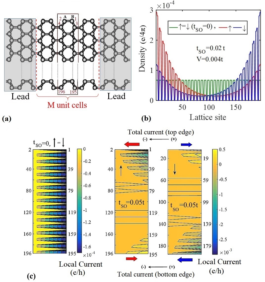
Further evidence of the QSH regime in transport is provided by the local spin-resolved charge current, shown in Fig. 2(c). More precisely, here we plot the bond current (calculated with Eq. 5) flowing through the horizontal dimers in the nanoribbon unit cell. The color scale is used to indicate both the direction and the intensity of the bond currents through the horizontal dimers of one unit cell (see Fig. 2(a) for the labeling of the dimer atoms). The apparent horizontal variation is related to the way we plot the intensity of this bond current for a given dimer, by inserting the total value of the current at one atom and going smoothly to zero to the other one. The unit cell is then repeated unchanged throughout the central part of the device. The potential drop of induces a net charge current from right to left. In the absence of SOI (left panel in Fig. 2(c)), the bond current is the same for spin-up and spin-down electrons and is rather homogeneously distributed throughout the nanoribbon. In contrast, when SOI is present, the bond current is mainly concentrated at the edges, where spin-up and spin-down electrons move in opposite directions. For example, at the top edge spin-up electrons (middle panel) move from right to left. At the same edge spin-down electrons (right panel) move from left to right, but their bond current is smaller than the bond current of the spin-up states, resulting in a net spin(-up)-polarized charge current from right to left. Similarly at the bottom edge we have a net spin(-down)-polarized charge current also flowing from right to left. Thus, we have a net bond charge current, localized at the two edges of the nanoribbon, where it is spin-polarized in opposite directions. Together with the quantization of the conductance and the spin accumulation at the edges, these properties of the spin-resolved current completely characterize the QSH state in this two-terminal geometry. As long as we remain in the QSH regime. For , the topological gap in bulk graphene vanishes and the system is no longer a QSH insulator.
III.2 Magnetic exchange fields: the QAH effect
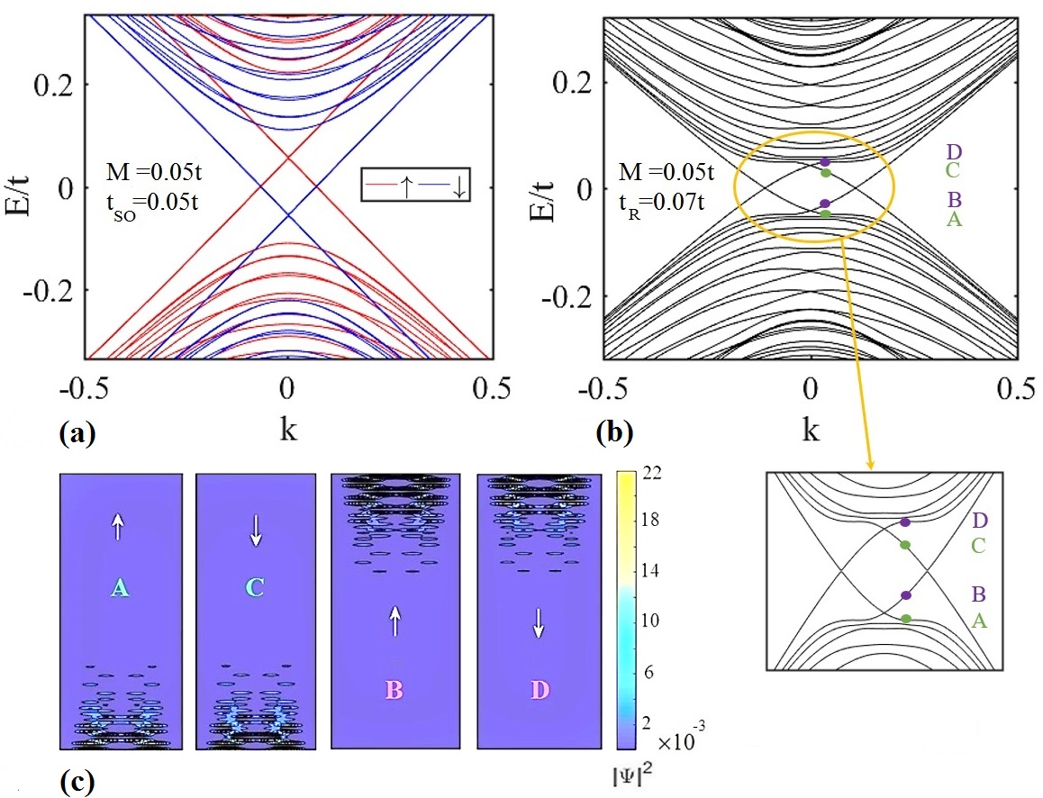
We now investigate the effect of adding a FM field that breaks TRS and can trigger a topological phase transition from the QSH to the QAH phase. In the absence of SOI (intrinsic and Rashba) a FM splits the two spin-degenerate Dirac cones and Dirac points with respect to each other. As a result of this splitting, the valence band of the spin-up states crosses the conduction band of the spin-down state at wave vectors . Suppose that only an intrinsic SOI is now switched on. Since this SOI does not couple opposite-spin states, it leaves these crossing points unaffected, but it opens a gap at the two Dirac points. In the resulting energy gap around , two pairs of linearly-dispersed helical edge states now appear. These are precisely the four helical states of Fig. 1(b) except that now the spin degeneracy is lifted by the FM exchange field, see Fig. 3(a). As for the case of zero exchange field, these four helical states give rise to the QSH effect, which therefore occurs even in the absence of TRS, when the only SOI present is of the spin-conserving intrinsic type 111According to Ref. Yang et al., 2011, there should be a transition to a QAH state for a critical value of a FM exchange field, even when . We don’t see this transition, since, when only intrinsic SOI is present, the FM field does not mix the spins and does not change the eigenstates..
The situation is different when a Rashba SOI is switched on. Let us consider first the case where this is the only SOI present (). Now the SOI couples opposite spin states, and therefore the level crossings between valence and conduction states, brought about by the FM exchange field, are replaced by avoided level crossings. The resulting bulk energy gap opening around has a topological nature very different from the one of the QSH phase, and so is also the case for the four linearly-dispersed edge states appearing in this gap, shown in Fig. 3(b) for a 196-AGNR. An analysis of these four branches reveals that they are 1D chiral edge states: the two branches localized at the same edge move in the same direction. This is shown in Fig. 3(c) where we plot the wavefunction space distribution inside the unit cell for four states with the same , belonging to the four edge channels. States A and C (B and D) belong to the two left(right)-mover branches and are localized at the bottom(tiop) edge. The two chiral states localized at the same edge have predominantly opposite spins, though the quantization is not perfect since spin is not conserved when Rashba SOI is present.
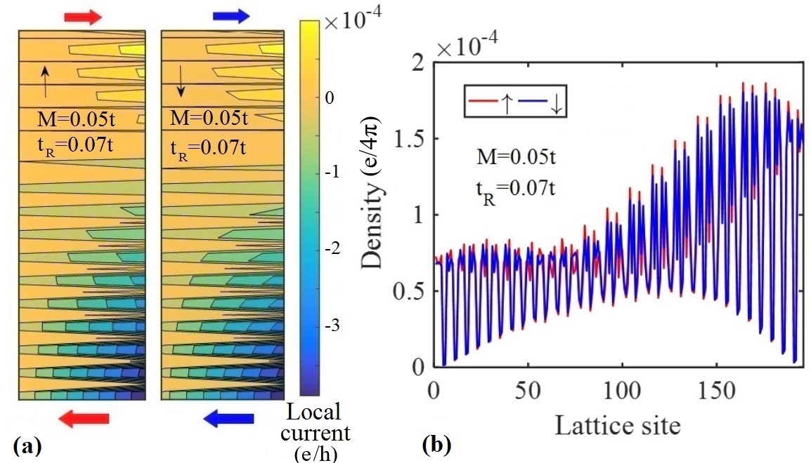
Based on the original edge-state approach to the quantum Hall effect introduced by Büttiker Büttiker (1988), the presence of two pairs of conducting chiral states at the edges signals the onset of a QAH phase, characterized in this case by a Chern number , leading to a quantized Hall conductance Yang et al. (2011). This occurrence is directly visible in the non-equilibrium two-terminal transport calculations. In Fig. 4(a), we plot the spin-resolved bond (charge) current in the nanoribbon unit cell, calculated using Eq. 5, for [Fig. 3(b)]. We can clearly see that the net current, going in this case from right to left, is due to the two spin-polarized conducting chiral edge states localized at the bottom edge, each contributing a quantized value to the Hall conductance. These bottom (left-mover) edge states, being injected from the ”source” electrode, will be at a higher chemical potential than the top edge states, and therefore will carry more current. The additional current is proportional to the increase of the 1D electron density at the top edge, as shown in Fig. 4(b), where we plot the non-equilibrium spin-resolved density inside the nanoribbon unit cell.
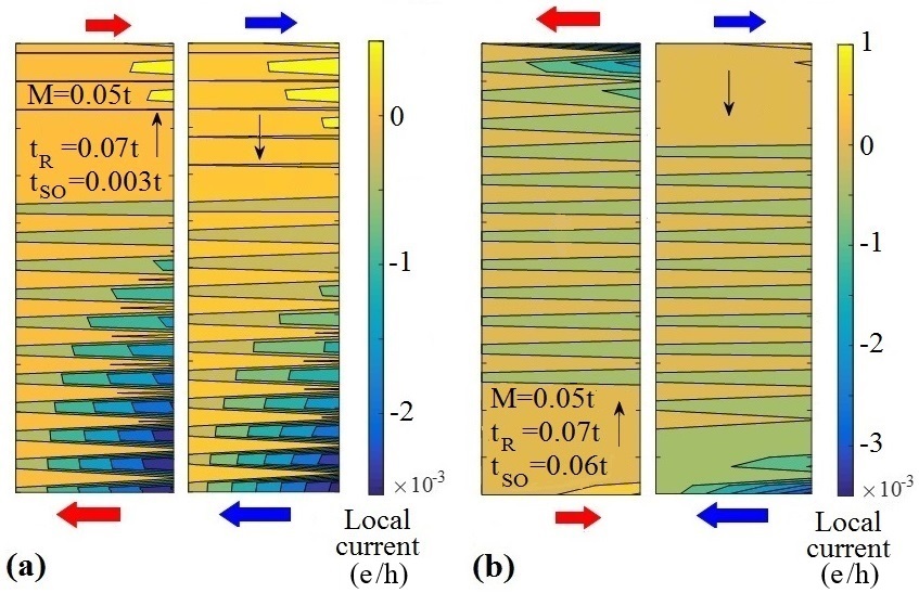
When in addition an intrinsic SOI is added, the two topological phases, QAH and QSH, start to compete. According to the Chern number analysis of Ref. Yang et al., 2011, when the ratio becomes larger than a magnetization-dependent critical value, the system undergoes a topological phase transition from a QAH phase to a QSH phase. This theoretical prediction is essentially consistent with our transport calculations, with an important caveat. In Fig. 5 we plot the local spin-resolved bond current for two values of for . As shown in Fig. 5(a) when , the system remains in the QAH phase. For (not shown), we find that a transition to a QSH phase has taken place. However, in the intermediate regime [Fig. 5(b)] although transport via helical edge states characteristic of the QSH phase is dominant, a non-zero bond current is present also in the middle of the nanoribbon, possibly due to states that are neither chiral non helical. This result might indicate that, for a finite-width nanoribbon, the transition between the QAH and QSH phases as function of occurs via a crossover regime rather than at a critical value .
We conclude by briefly discussing the effect of an AFM exchange field, which when added to the Hamiltonian of Eq. 1, breaks both TRS and inversion symmetry , but preserves the combination of the two. In particular, the AFM field preserves the symmetry , where is the lattice translational symmetry swapping the two graphene sublattices. This occurrence is similar but not identical to the one considered in Ref. Mong et al., 2010, where the combined symmetry involved the product of and , the lattice translational symmetry of the ”primitive” structural lattice broken by the AFM order. For this case the system is a topological phase called AFM TI, which shares some properties of the ”strong” topological insulators. On the other hand, our calculations for an AGNR in the presence of AFM exchange and Rashba SOI show that for the spectrum has a bulk energy gap centered at , and the system is a trivial insulator. At the gap closes with flat bands at and opens again for . However, no topological chiral edge states ever emerge in such a gap and the system remains a trivial insulator. Thus, in the presence of an AFM TRS-breaking field, the system can only display a QSH phase, which happens when .
IV CONCLUSIONS
We have carried out non-equilibrium quantum transport calculations on armchair graphene nanoribbons in a two-terminal geometry in the presence of spin-orbit interactions (SOIs) and TRS-breaking exchange fields. Depending on the relative strength of these interactions, the system can sustain both a quantum spin Hall (QSH) and a quantum anomalous Hall (QAH) regime. Both phases are completely characterized by the nature of their conductive topological edge states, which control the electronic transport and display specific features in the spin-resolved local current and out-of-equilibrium charge density. In the presence of a FM exchange field, it is possible to trigger a topological phase transition from a QAH phase to a QSH phase by changing the relative strength of the intrinsic and Rashba SOI. Therefore the QSH phase can survive even in the absence of TRS.
V Acknowledgments
This work was supported by the Faculty of Technology and by the Department of Physics and Electrical Engineering at Linnaeus University (Sweden). We acknowledge financial support from the Swedish Research Council (VR) through Grant No. 621-2014-4785, and by the Carl Tryggers Stiftelse through Grant No. CTS 14:178. Computational resources have been provided by the Lunarc Center for Scientific and Technical Computing at Lund University. CMC acknowledges valuable interactions with A.H. MacDonald.
References
- Qi and Zhang (2010) X. L. Qi and S. C. Zhang, Phys. Today 63, 33 (2010).
- Kane and Mele (2005a) C. L. Kane and E. J. Mele, Phys. Rev. Lett. 95, 226801 (2005a).
- Kane and Mele (2005b) C. L. Kane and E. J. Mele, Phys. Rev. Lett. 95, 146802 (2005b).
- Min et al. (2006) H. Min, J. E. Hill, N. A. Sinitsyn, B. R. Sahu, L. Kleinman, and A. H. MacDonald, Phys. Rev. B 74, 165310 (2006).
- Boettger and Trickey (2007) J. C. Boettger and S. B. Trickey, Phys. Rev. B 75, 121402 (2007).
- König et al. (2007) M. König, S. Wiedmann, C. Brune, A. Roth, H. Buhmann, L. W. Molenkamp, X. L. Qi, and S. C. Zhang, Science 318, 766 (2007).
- Klimovskikh et al. (2017) I. I. Klimovskikh, M. M. Otrokov, V. Y. Voroshnin, D. Sostina, L. Petaccia, G. D. Santo, S. Thakur, E. V. Chulkov, and A. M. Shikin, ACS Nano 11, 368 (2017).
- Yang et al. (2011) Y. Yang, Z. Xu, L. Sheng, B. Wang, D. Y. Xing, and D. N. Sheng, Phys. Rev. Lett. 107, 066602 (2011).
- Haldane (1988) F. D. M. Haldane, Phys. Rev. Lett. 61, 2015 (1988).
- Qiao et al. (2010) Z. Qiao, S. A. Yang, W. Feng, W.-K. Tse, J. Ding, Y. Yao, J. Wang, and Q. Niu, Phys. Rev. B 82, 161414 (2010).
- Qiao et al. (2014) Z. Qiao, W. Ren, H. Chen, L. Bellaiche, Z. Zhang, A. MacDonald, and Q. Niu, Phys. Rev. Lett. 112, 116404 (2014).
- Topinka et al. (2003) M. A. Topinka, R. M. Westervelt, and E. J. Heller, Phys. Today 56, 47 (2003).
- Crooker et al. (2005) S. A. Crooker, M. Furis, X. Lou, C. Adelmann, D. L. Smith, C. J. Palstrom, and P. A. Crowell, Science 309, 2191 (2005).
- Walz et al. (2014) M. Walz, J. Wilhelm, and F. Evers, Phys. Rev. Lett. 113, 136602 (2014).
- Konschuh et al. (2010) S. Konschuh, M. Gmitra, and J. Fabian, Phys. Rev. B 82, 245412 (2010).
- andFeng-feng Zhu et al. (2015) F. Z. andFeng-feng Zhu, W. jiong Chen, Y. Xu, C. lei Gao, D. dan Guan, C. Liu, D. Qian, S.-C. Zhang, and J. feng Jia, Nat. Mat. 14, 1020 (2015).
- Xiong et al. (2016) W. Xiong, J. D. T. W. J. Z. Congxin Xia, Yuting Peng, and Y. Jiac, Phys. Chem. Chem. Phys. 18, 6534 (2016).
- Wang et al. (2016) T.-C. Wang, F.-C. C. W.-S. S. Chia-Hsiu Hsu, Zhi-Quan Huang, and G.-Y. Guo, Sci. Rep. 6, 39083 (2016).
- Datta (1997) S. Datta, Electronic Transport in Mesoscopic Systems (Cambridge Studies in Semiconductor Physics and Microelectronic Engineering) (Cambridge University Press, 1997).
- Lopez Sancho et al. (1984) M. P. Lopez Sancho, J. M. L. Sancho, and J. Rubio, Jour. of Phys. F: Met. Phys. 14, 1205 (1984).
- Cresti et al. (2003) A. Cresti, R. Farchioni, G. Grosso, and G. P. Parravicini, Phys. Rev. B 68, 075306 (2003).
- Mahfouzi and Nikolić (2013) F. Mahfouzi and B. K. Nikolić, SPIN 3, 1330002 (2013).
- Nikolić et al. (2006) B. K. Nikolić, L. P. Zârbo, and S. Souma, Phys. Rev. B. 73, 075303 (2006).
- Zârbo and Nikolić (2007) L. P. Zârbo and B. K. Nikolić, EPL 80, 47001 (2007).
- Chen et al. (2010) S.-H. Chen, B. K. Nikolić, and C.-R. Chang, Phys. Rev. B. 81, 035428 (2010).
- Todorov (2002) T. N. Todorov, J. Phys.: Condens. Matter 14, 3049 (2002).
- Caroli et al. (1971) C. Caroli, R. Combescot, P. Nozieres, and D. Saint-James, J. Phys. C: Solid State Phys. 4, 916 (1971).
- Note (1) According to Ref. \rev@citealpYang2011, there should be a transition to a QAH state for a critical value of a FM exchange field, even when . We don’t see this transition, since, when only intrinsic SOI is present, the FM field does not mix the spins and does not change the eigenstates.
- Büttiker (1988) M. Büttiker, Phys. Rev. B 38, 9375 (1988).
- Mong et al. (2010) R. S. K. Mong, , A. M. Essin, and J. E. Moore, Phys. Rev. B 81, 245209 (2010).