Weakly Trapped, Charged, and Free Excitons in Single-Layer MoS2 in Presence of Defects, Strain, and Charged Impurities
Abstract
Few- and single-layer MoS2 host substantial densities of defects. They are thought to influence the doping level, the crystal structure, and the binding of electron-hole pairs. We disentangle the concomitant spectroscopic expression of all three effects, and identify to which extent they are intrinsic to the material or extrinsic to it, i.e. related to its local environment. We do so by using different sources of MoS2 — a natural one and one prepared at high pressure and high temperature — and different substrates bringing varying amounts of charged impurities, and by separating the contributions of internal strain and doping in Raman spectra. Photoluminescence unveils various optically-active excitonic complexes. We discover a defect-bound state having a low binding energy of 20 meV, that does not appear sensitive to strain and doping, unlike charged excitons. Conversely, the defect does not significantly dope or strain MoS2. Scanning tunneling microscopy and density functional theory simulations point to substitutional atoms, presumably individual nitrogen atoms at the sulfur site. Our work shows the way to a systematic understanding of the effect of external and internal fields on the optical properties of two-dimensional materials.
keywords:
MoS2, 2D materials, Raman spectroscopy, photoluminescence, electronic transport, scanning tunneling microscopy, defects, doping, optical contrastUniv. Grenoble Alpes] Univ. Grenoble Alpes, CNRS, Institut Néel, 38000 Grenoble, France \altaffiliationThese authors contributed equally to this work Univ. Grenoble Alpes] Univ. Grenoble Alpes, CNRS, Institut Néel, 38000 Grenoble, France \altaffiliationThese authors contributed equally to this work Univ. Grenoble Alpes] Univ. Grenoble Alpes, CNRS, Institut Néel, 38000 Grenoble, France \altaffiliationThese authors contributed equally to this work Univ. Grenoble Alpes] Univ. Grenoble Alpes, CNRS, Institut Néel, 38000 Grenoble, France Univ. Grenoble Alpes] Univ. Grenoble Alpes, CNRS, Institut Néel, 38000 Grenoble, France Univ. Grenoble Alpes] Univ. Grenoble Alpes, CNRS, Institut Néel, 38000 Grenoble, France Univ. Grenoble Alpes] Univ. Grenoble Alpes, CNRS, Institut Néel, 38000 Grenoble, France CEA SPEC] SPEC, CEA, CNRS, Université Paris-Saclay, CEA Saclay, 91191 Gif-sur-Yvette Cedex, France \altaffiliationDepartamento de Física Teórica de la Materia Condensada and Condensed Matter Physics Center (IFIMAC), Facultad de Ciencias. Universidad Autonoma de Madrid, E-28049 Madrid, Spain CEA SPEC] SPEC, CEA, CNRS, Université Paris-Saclay, CEA Saclay 91191 Gif-sur-Yvette Cedex, France NIMS] National Institute for Materials Science, Tsukuba, 305-0044, Japan NIMS] National Institute for Materials Science, Tsukuba, 305-0044, Japan Univ. Grenoble Alpes] Univ. Grenoble Alpes, CNRS, Institut Néel, 38000 Grenoble, France Univ. Grenoble Alpes] Univ. Grenoble Alpes, CNRS, Institut Néel, 38000 Grenoble, France Univ. Grenoble Alpes] Univ. Grenoble Alpes, CNRS, Institut Néel, 38000 Grenoble, France LMA] Laboratorio de Microscopías Avanzadas, Instituto de Nanociencia de Aragón, Universidad de Zaragoza, 50018 Zaragoza, Spain \altaffiliationARAID Foundation, 50018 Zaragoza, Spain Univ. Grenoble Alpes] Univ. Grenoble Alpes, CNRS, Institut Néel, 38000 Grenoble, France Univ. Grenoble Alpes] Univ. Grenoble Alpes, CNRS, Institut Néel, 38000 Grenoble, France Univ. Grenoble Alpes] Univ. Grenoble Alpes, CNRS, Institut Néel, 38000 Grenoble, France Univ. Grenoble Alpes] Univ. Grenoble Alpes, CNRS, Institut Néel, 38000 Grenoble, France Univ. Grenoble Alpes] Univ. Grenoble Alpes, CNRS, Institut Néel, 38000 Grenoble, France
Main text
Single-layer molybdenum disulphide (MoS2) is a widely-studied candidate for future optoelectronics, where energy conversion is achieved with much lesser amounts of matter than with traditional three-dimensional materials, and a wealth of functionalities emerge from flexibility and transparency.1 The direct band-gap in the electronic band structure2 is the key to light emission3, 4 and conversion5 in single-layer MoS2. Due to the reduced dimensionality, Coulomb interactions play a key role in this system and lead to a large exciton binding energy. More generally this system is a playground for testing many-body Coulomb interaction theories that should be able to describe excitonic complexes.6, 7, 8 The current understanding is that the excitons in monolayer transition metal dichalcogenides have fast radiative lifetimes9, 10, 11 (sub-picosecond) and that the interlayer excitons in type-II junctions are long lived12, 13 (in the nanosecond range at low temperature). Such excitons could be used for light-emission or light-harvesting devices, respectively. In both cases the presence of defects will induce non-radiative decay, reducing device efficiency, and/or modify the exciton emission energy. A chemical treatment eliminating defects allowed to demonstrate a photoluminescence quantum yield close to unity, and long lifetimes.14 Nevertheless the nature of defects in non-treated samples and their role in radiative and non-radiative recombination remain as open questions. To bring clearcut answers to this pressing question, well-characterised defects need to be investigated and their influence on the physical properties need to be understood. They could be intrinsic to the single-layer, e.g. sulfur vacancies and substitutional atoms,15, 16, 17, 18, 19, 20, 21, 22, 23, 24 or extrinsic to it, in the form of charged impurities, either trapped in the MoS2 substrate19 or adsorbed on it.25, 26, 27, 28 The latter is thought to limit the electronic mobility of MoS2-based transistors below the phonon-limited value.29
Here, we report on point defects that induce defect-bound excitons in single-layers of MoS2. The MoS2 is obtained from two different sources of bulk crystals. We use a natural crystal and a synthetic crystal, prepared at high pressure and high temperature (denoted HP/HT in the following). We find that the latter kind of bulk MoS2 hosts specific defects, and holds promise for improved control of the structure of MoS2 in the future. We discriminate the electronic doping, mechanical strain, and defect-induced exciton localisation by combining Raman spectroscopy, photoluminescence mapping, scanning tunneling microscopy (STM), and density functional theory (DFT) calculations. We also discriminate the influence of extrinsic and intrinsic effects by addressing samples transfered on silica and on hexagonal boron nitride (h-BN).
Preparation of MoS2 few- and single-layers. The natural MoS2 bulk crystals (typical size, 2 mm) used in this study are provided by SPI-supplies. The second kind of bulk MoS2 we used are prepared at NIMS, Tsukuba, following a slow cooling process from a molten state attained under high pressure. Here, MoS2 (99.9% pure), supplied by Kojund Chemical Laboratory Co. Ltd., is encapsulated in a h-BN capsule and brought to 5 GPa and 1800∘C for 20 min by using a belt-type high pressure apparatus. The sample is then cooled down to room temperature at a rate of 0.8∘C/min. After releasing the pressure, the MoS2 crystal is recovered by crushing the h-BN capsule. The crystal size after this process is typically 1 mm.
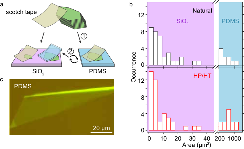
Mechanical exfoliation of MoS2 was achieved with two processes (Figure 1a). In the first one, a macroscopic MoS2 grain attached onto scotch-tape is thinned down with repeated scotch-tape exfoliation. Next the surface of the MoS2-covered tape is stamped onto a SiO2 wafer.30 Irrespective of the source of MoS2, the typical area is of the order of few 1 to 10 m2 (Figure 1b). The other process, using a polydimethylsiloxane (PDMS) host support31 instead of SiO2, substantially increases the area of the exfoliated flakes, in the few 100 to 1,000 m2 range (Figure 1b). Figure 1c displays a photograph of one of the largest flakes (a bi-layer one) that we exfoliated, among the several tens we have prepared. We note that the transfer processes that we used are dry-process that are not expected to alter the atomic structure of the individual MoS2 layers. The use of PDMS limits the amount of contaminants left on MoS2,31 as observed by atomic force microscopy and electron energy loss spectroscopy performed in a scanning transmission electron microscope (see Supporting Information, Figures S1,S2).
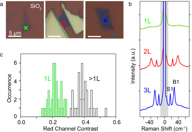
As a preliminary step, we present the way we determine the thickness of the flakes. Our approach is to establish the correspondence between optical contrast, which varies with the number of layers and optical wavelength in a rather complex manner32, 33 (Figure S3), and an unambiguous independent determination of the number of layers with Raman spectroscopy. We track the occurrence and position of the shear (S1) and breathing (B1) interlayer vibrational modes.34, 35 Figure 2a shows three MoS2 flakes exfoliated with scotch-tape onto SiO2. Their Raman spectra are different, with the single-layer MoS2 readily identified by the absence of the B1 and S1 modes, while these two modes are found in bi- and tri-layers, and are stiffer in the latter case (Figure 2b). We find that in the red-channel of the digital optical images, the contrast is the lowest, of 0.220.08 for a single-layer (Figure 2c). This characteristic contrast value is used as a criterion for fast identification of single-layers. The remaining of the paper is focused on single-layers.
Using PDMS stamps where single-layers are first identified, we then transferred MoS2 onto two kinds of substrates. The first one is SiO2, and the second one is h-BN, which has been exfoliated onto SiO2 beforehand. In both processes, the interface between MoS2 and the substrate has not been exposed to the polymer (PDMS), hence pristine MoS2/support interfaces are formed.
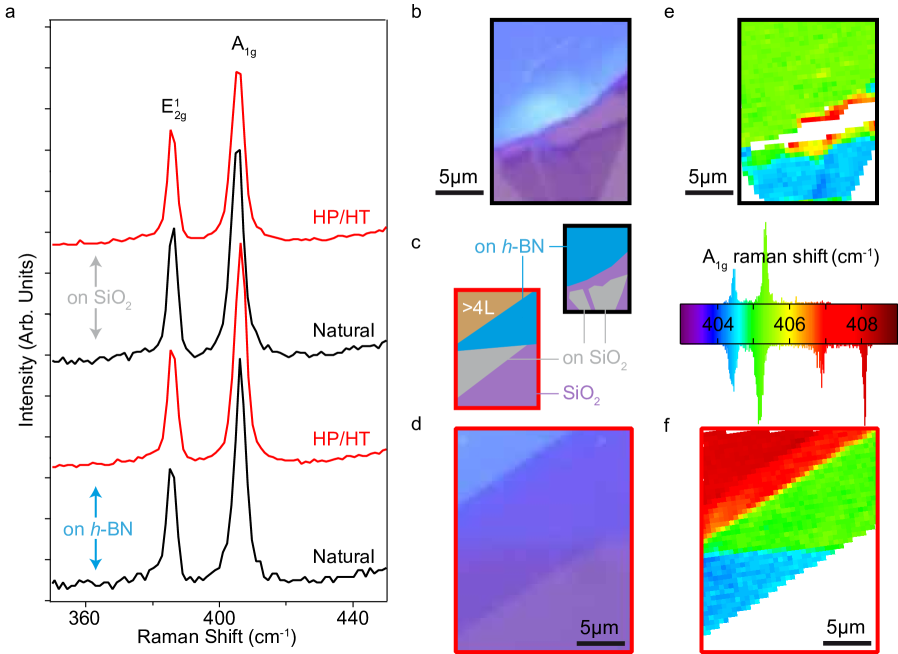
Strain and electronic doping from vibrational spectroscopy. Figure 3a shows characteristic Raman spectra zoomed in the low wavenumber region, featuring intralayer shear (E) and breathing (A1g) modes (which are stiffer than the interlayer modes addressed above, for which the bond strength is much lower), for the two sources of MoS2 on the two substrates. To better highlight the differences between the four possible stacks (on the two substrates, for each of the two sources), we mapped the position of the A1g mode (determined by Lorentzian fits of the corresponding peak), which is especially sensitive to electron-phonon coupling effects,36 across an area corresponding to the optical micrographs shown in Figures 3b-d. The result is shown in Figures 3e,f. The most obvious difference is the correlation between the position of the A1g mode and the nature of the substrate: a blue-shift, of 1.00.1 and 0.80.1 cm-1 from the SiO2 to the h-BN substrate, is observed for the natural and HP/HT sources respectively.
These blue shifts may be caused by mechanical strain37, 38, 39 and/or by electron doping,36 translating the anharmonicity of the interatomic potentials and the effect of the electron-phonon interaction respectively. The energy of the A1g and E modes have characteristic variations with each of the effect. A strain vs doping graph can hence be extracted from the maps of the A1g (Figures 3e,f) and E Raman shifts — a two-dimensional space is constructed with the positions of the A1g and E modes as principal axis.40 Figure 4 shows such a graph for the two samples. Disregarding at this stage the colours of the points (which will be discussed later in the light of the photoluminescence measurements), for both samples we find two groups of points, each corresponding to MoS2 on h-BN (greater A1g positions) and on SiO2. The trend is similar for both sources of MoS2, suggesting that the observations mostly point to an extrinsic effect, namely the nature of the substrate. The electron doping level is larger by 2.5 and 2.0 electrons/cm-2 on SiO2, for the natural and HP/HT sources respectively. Substrate-induced doping is a known phenomena, which was ascribed, in other two-dimensional materials,41, 42, 43 to charged impurities in SiO2 that are absent in h-BN. These charged impurities effectively dope MoS2 with electrons, and the observed doping level is consistent with a previous observation44 — they hence represent extrinsic defects.
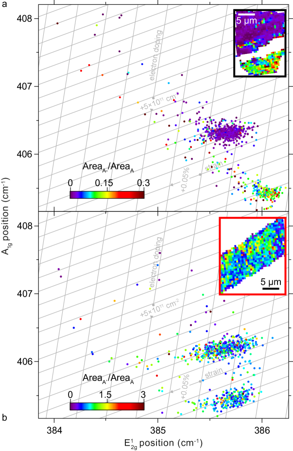
Figures 4a,b also reveal that the transfer process can generate non-uniform strains to small extent. The two clusters of points from both images are scattered within typically 0.05 to 0.1%. Besides, in the case of Figure 4a (natural source of MoS2), a strain difference of 0.05 to 0.1% is found between the two clusters of points, corresponding to the top and bottom part of the optical image (on h-BN and SiO2 respectively). We do not find such a difference in Figure 4b (HP/HT-MoS2). The observed differences are not systematic, and we believe that they point to slightly different mechanical efforts exerted during the preparation and/or different h-BN thicknesses for the two samples, rather than from, e.g., internal strain induced by defects.39
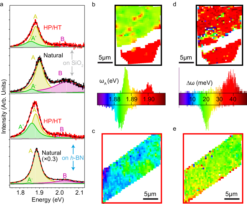
Excitonic complexes in presence of strain, electronic doping, and defects. Both electronic doping level and strain influence the excitonic properties of MoS2.45, 46, 47, 48, 37 To address these effects we performed photoluminescence measurements at room temperature with a 532 nm laser excitation and low power (see Materials and Methods) for both sources of MoS2 and both substrates. Figure 5a displays characteristic spectra corrected from optical interference effects (special care needs to be paid to these corrections, see Supporting Information, Figures S3,S4). As expected with an excitation wavelength of 532 nm, two main excitonic peaks are observed, each corresponding to a different transition involving one or the other spin-polarized valence band.49 In the following, we will focus on the lowest energy peak, and to start with, we address the natural source of MoS2. This peak actually comprises two components. They are separated by typically 40 meV and have a full-width at half maximum of several 10 meV dominated by electron-phonon coupling effects.50 They correspond to a neutral (A) exciton and a charged (A-) exciton — a trion.45, 51 The latter is more prominent when the electronic doping is higher.45
As discussed in Ref. 45, the ratios of areas of the two peaks as inferred from photoluminescence (Figure 4a) characterise the level of electron doping; we estimate it to be typically of the order of several 1012 electrons/cm-2. The inset of Figure 4a reveals a distinctive trion vs exciton population whether MoS2 lies on SiO2 or h-BN. The ratios of A- to A areas, typically 0.01-0.02 and 0.1 respectively on these two substrates, are consistent with changes of electronic doping levels, due to charged impurities in SiO2, found in the analysis of the Raman data (of the order of a few cm-2).
The position of the two peaks (Figures 5b,S5) is changing by 12 meV whether MoS2 lies on SiO2 or h-BN. As Raman spectroscopy suggests, this is a result of the preparation process causing a spatial strain variation, a compression on SiO2 relative to the case on h-BN, by about 0.1%. The magnitude of the strain-induced energy shift fits with that corresponding to previously reported strain-induced electronic band-gap change.37
Let us now turn to the photoluminescence signatures in case of HP/HT-MoS2. In this case also, we find that the main excitonic feature does not consist of a single component. While the above-discussed energy difference between the two componenents was about 40 meV for natural MoS2, consistent with the expected trion binding energy corresponding to electron doping levels of the order of few electrons/cm-2,45 here the two components are separated by a substantially lower energy difference (20 meV), regardless of the substrate (Figure 5c). Such an energy difference cannot correspond to a trion under the influence of strain or electronic doping: the variations of strain and electronic doping in our samples are in the range of few 0.1% and 1012 cm-2 respectively, which have only marginal influence on the binding energy of the trion (few 1 meV or below).52, 45 What is then the nature of this low-energy emission?53 Its spectral weight is globally high and strikingly, unlike the A- feature for natural MoS2, does not corelate with the kind of substrate, and corresponding doping level revealed by Raman spectroscopy (Figure 4b). This is at variance to the behaviour expected for trions.
A rational explanation for this low-energy feature (in the case of HP/HT MoS2) is that it relates to a defect-bound exciton. Defect-bound excitons were previously invoked in MoS2 and attributed to sulfur vacancies, di-vacancies, and metal vacancies.17, 54 While they were found to be associated with a binding energy of the order of 100 meV, here we find a binding energy of 20 meV. The limited variations of strain or electronic doping in our samples do not allow us to reveal a possibly different influence of these effects on the A’, A- and A features. As we will see, samples from the HP/HT source comprise a larger amount of defects. In the following, we devise on the nature and density of these defects using additional probes.
The nature of the point defects. A large variety of defects has been considered in MoS2, including sulfur vacancies,16, 17, 18, 23 substitutional atoms replacing either the metal or the sulfur atom,15, 16, 17, 18, 22, 23 and individual atoms (the electrodonor alkali atoms) adsorbed onto the surface.15 Only the latter kind has been reported to be associated to shallow donor levels, that could account for usually reported -doping in single-layer MoS2 at room temperature. The chemical analysis of the starting material in the HP/HT process does not seem compatible with the presence of alkali atoms, though. On the contrary, based on this analysis, potential candidates as impurities are iron and carbon prominently, or boron and nitrogen from the capsule used to seal the MoS2 during the HP/HT treatment.
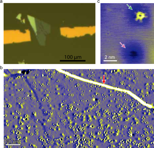
The impurity levels in MoS2 are too low to be reliably assessed with standard macroscopic chemically-sensitive probes such as X-ray photoelectron spectroscopy.21 High resolution microscopy circumvents this issue, by addressing the defects individually. We used STM for this purpose, as implemented in a ultra-high vacuum environments that limits spurious interactions of the defects with e.g. small molecules. Very few reports in the literature have in fact been devoted to STM measurements on single- or few-layer flakes. Mostly, this is due to the small size (few 1 to 10 m2) of the exfoliated flakes, which if deposited on a non-conductive substrate, must be electrically contacted with finely designed electrodes. The observation of such small features with a short-field-of-view-technique as STM is obviously very laborious. This is probably why most reports since 20 years rely on cleaved bulk MoS2.55, 56, 57, 21, 58, 20, 19 Two workarounds have been recently implemented: one, taking benefit of large-area growth of MoS2 on graphite,59, 60 and the other the strong adhesion of MoS2 exfoliated on a gold surface.61 As far as we are concerned, we chose an alternative strategy and once more exploited PDMS exfoliation (Figure 1a) which yields large flakes of sizes approaching 100 m, using as a host substrate a (conductive) graphene-covered silicon carbide surface. To ease the localisation of the (few-layer) flake we further deposited micrometer-sized gold markers (Figure 6a, see Methods and Materials).
This rather advanced sample preparation allows to image single defects with STM (yet it should be noted that the measurements are in no way straightforward). A high density of defect is observed (Figure 6b), of the order of 11012 cm-2, varying from 0.6 to 41012 cm-2 from one place to the other. A spatially inhomogeneous distribution of defects was already quoted in previous STM analysis from MoS2 samples.58, 21, 62 The density we find on the HP/HT sample is larger than the one observed on samples prepared by exfoliation of natural molybdenite, which is in the few 1011 cm-2 range58, 21 or less19 (3.51010 cm-2). Conversely, a much larger density of defects (from 51012 cm-2 to 51013 cm-2) has been reported for MoS2 prepared by exfoliating synthetic crystals.62
In the HP/HT MoS2 we find two prominent populations of point defects, which appear as a bright feature and a depression respectively (Figure 6c). Depression-like defects of the same extension (1-2 nm) or slightly larger (in the few nanometer-scale) have been reported previously.63, 55, 21, 58, 19. Among them, one appears as a depression at negative tip-sample bias as in our observations, and is a characteristic defect in natural MoS2 that is ascribed to missing S-Mo-S fragments located either in the top or in a buried MoS2 layer.58 The second kind of defect (the bright one) has not been observed in natural MoS2 samples, and is hence generated during the preparation of the HP/HT sample. It has a characteristic shape resolved with sharp STM tips, consisting in a ring with three pairs of radial legs. The size of the ring is typically 0.7 nm. Defects featuring a ring shape in STM have also been reported previously55, 56 and were ascribed to alkali atoms adsorbed on the surface. Nor the HP/HT process neither the ultra-high vacuum chamber where the STM measurements were performed seem to yield such adsorbates, though.
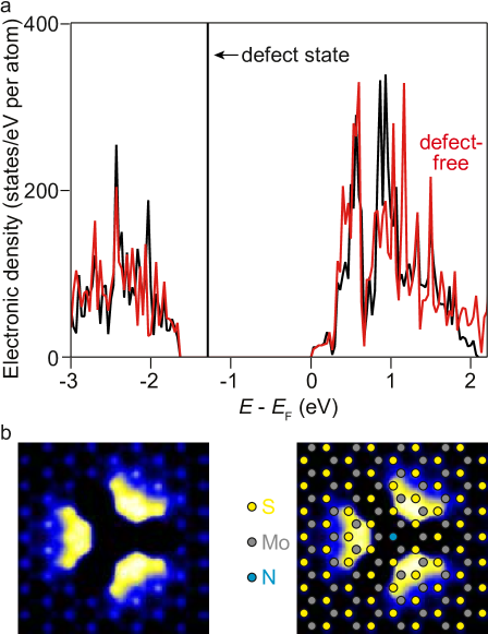
Both electronic and structural information contribute to STM images. To devise on the nature of the defects, DFT simulations provide key insights to interpret the observed STM contrasts. The comparison of experimental STM images with spatially-resolved information provided by DFT is a well-established approach to study defects. To our knowledge such comparison has not been made in the case of defects in MoS2 beyond the case of lattice vacancies.63, 62 We computed the stable configurations of five defects corresponding to the impurities that are detected in the chemical analysis of the raw MoS2 or present in the h-BN capsule used in the HP/HT process. This includes a sulfur vacancy, a molybdenum atom substituted by an iron atom, an a sulfur atom substituted by a carbon, a nitrogen, and a boron atom. Each of these defects are associated with electronic states inside the bandgap of MoS2 (here expectedly close to the bulk value of 1.3 eV) or close to the bandgap edges (see Figures 7a,S7). The sample bias of -2.0 V corresponds to electrons tunneling from the sample to the tip, in an energy window of 2.0 eV below the MoS2 Fermi level, which is presumably located close to the conduction band minimum. It is thus expected that the defect electronic states within the bandgap have significant contribution compared to the valence band, given that they correspond to a lower tunnel barrier. We simulated STM images by taking into account the STM tip (see Materials and Methods) in presence of the different defects. The results are shown in Figure S8, and for one specific defect (nitrogen atom substituting a sulfur atom) in Figure 7b. For the latter defect, the simulated STM image is in rather good agreement with the experimental one, despite the significant difference in spatial resolution, which is higher in the simulations. Indeed in the experiment, an Ångström-scale instability of the scanning tip is observed (as shown by the occurence of horizontal stripes at the defect location in Figure 6c), and the tip’s shape presumably deviates from the ideal pyramidal shape assumed in the calculations. We consider this as the reason why the three brilliant lobes observed in the simulated image appear as a circle in the experimental image. Beyond this, the main features compare very well for the N substitutional defect: the size of the lower-intensity central feature match, and the three pairs of legs appearing in the experimental image seem reminiscent of the three lobes found in the simulations. Based on this comparison we propose that the ring-shaped defects we observed correspond to nitrogen atoms having replaced sulfur ones during the HP/HT sample preparation (and originating e.g. from the h-BN capsule used in this process).
Field-effect transistor based on HP/HT MoS2. Single-layer MoS2 prepared under HP/HT conditions was finally integrated into a field effect transistor with electrostatic gating from the back-side, in which direct contact with SiO2 was avoided by a h-BN buffer layer (Figure 8). Accordingly a low amount of charged impurities is expected in the vicinity of MoS2. Consistent with previous reports, we find that the conduction properties are improved under vacuum (compared to ambient pressure), presumably due to the desorption of species acting as charged impurities.27 We only observe the blocked state of the transistor and the regime of electron conduction (and not the hole conduction regime) in the source-drain current vs gate-voltage characteristic (Figure 8).
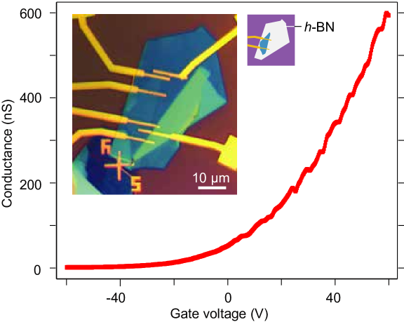
The transport properties overall show very typical semiconducting properties which match those found in similar devices based on natural MoS2. We estimate the threshold voltage to be at a gate voltage of 10 V. The mobility from the gating curve is estimated to be 2 cm2V-1s-1 (the device in the on-state has not reached saturation in the range of applied gate-voltage, so this value is a lower-estimate). These two values are similar to those found in devices using the same geometry based on natural MoS2, and more recently in similar field-effect transistor architecture featuring single-layer MoS2 synthesised by chemical vapor deposition transfered onto h-BN.64, 65 In all these works and ours, we stress that the Schottky barriers at the Au/MoS2 junctions under the source and drain electrodes play a dominant role in the low-value-mobility obtained from the two-probe measurement; in other words the defects that are present in the MoS2 channel are not limiting transport in this configuration.
Conclusions
Using Raman spectroscopy, photoluminescence spectroscopy, scanning tunneling microscopy, density functional theory, and electronic transport measurements, we addressed the optoelectronic properties of MoS2 single-layers prepared by exfoliation from two different sources of bulk material — a natural one, and another one prepared under high-pressure and high-temperature (HP/HT) conditions. The latter preparation process opens the route to the control of the structure of MoS2, in terms of intentional generation of otherwise inaccessible defects and possibly in the future as well in terms of superior quality, namely increased single-crystal size and lower defect (e.g. vacancies) concentration as was achieved with h-BN.66 This holds promise for close-to-ideal support for other two-dimensional materials67 and high-performance optoelectronic devices. Natural and HP/HT both have a substantial electron-type doping, of the order of 1012 cm-2, which is stronger on SiO2 substrates than on h-BN, due to a lower amount of extrinsic charged impurity in the latter case. Additional defects are present in HP/HT MoS2. We argue that they lead to defect-bound excitons, with a few 10 meV binding energy. We propose that these defects are nitrogen atoms substituting sulfur atoms. Exploring the nature of the localisation potential associated to the defects, and its effects on the coupling to the electromagnetic field, will provide valuable insights to understand light-matter coupling in transition metal dichalcogenides. In addition, the defect-bound exciton we discover may couple coherently with the neutral exciton. Stronger coupling and larger coherent times than reported in MoSe2 at low temperature between excitons and trions68 might result from the weak trapping of the defect-bound exciton. On a general note, our work also sheds light on the influence of defects on the optoelectronic properties of these two-dimensional materials and their interplay with internal and external (force, electric, optical) fields.
Materials and methods
Mechanical exfoliation. Si/SiO2 substrates with 285 nm-thick oxide were cleaved into 1 cm 1 cm pieces. They were cleaned using acetone and isopropyl-alcohol, followed by a dry nitrogen blow. The substrates were subjected to a oxygen plasma for 3 to 4 minutes. For mechanical exfoliation, small pieces of MoS2 crystal were placed on the scotch tape followed by repeated exfoliation. The tape was then stamped on to the Si/SiO2 substrate, then it was then heated for 15-30 s at 80-100∘C on a hot plate. The tape was then gently removed from the substrate at an angle of 60 to 70∘. A similar process was followed on the PDMS substrate, without the application of heat. For the MoS2/hBN heterostructures, a PDMS stamping method was used.31
Raman spectroscopy and photoluminescence measurements. Raman spectroscopy and photoluminescence were acquired with 532 nm Nd:YAG laser using a commercial confocal WITEC spectrometer at room temperature under ambient condition. The laser spot size was 1 m. The signal was collected through a 50 objective with a numerical aperture of 0.75. For the Raman spectra, the power was kept at 300 W to avoid damage due to laser-induced heating in MoS2 flakes. The signal was integrated for 2 s after being dispersed by a 1800 lines/mm grating. For photoluminescence measurements, a low power of 8 W (see Supporting Information and Figure S6) was used with a grating of 600 lines/mm. The photoluminescence spectra were taken with an integration time of 30 s to improve signal-to-noise ratio, and the spatially-resolved photoluminescence maps were taken with an integration time of 5 s.
Optical images have been acquired in a Zeiss microscope equipped with a digital camera "axiomcam 105 colour" device, a tungsten halogen light source and with a magnification of 100. The white balance has been set to the expected one for an halogen lamp at 3200 K.
To allow for fast determination of the flakes number of layers (less than four layers) across square centimeter-scale surfaces, we determined the value of a representative optical quantity for flakes of known (from Raman spectroscopy) thickness. We chose the contrast of the RBG images, with respect to the surrounding SiO2 surface, in red channel (red channel contrast, RCC) as a relevant quantity, defined as the difference between the signal from SiO2 () and from the flake (), normalised by :
Fabrication and measurement of MoS2 FET device. The substrate for FET was degenerately-doped silicon with 285 nm of SiO2 on which h-BN flakes were exfoliated. The single-layer MoS2 flake was deterministically transferred on h-BN using PDMS. Two-step electron-beam lithography followed by metal deposition was used next: in the first step 5 nm of Ti and 65 nm of Au were deposited for the outer pads, and in the second step, 100 nm of Au was used to contact MoS2. The FET measurement was performed at room temperature under vacuum in a probe station.
Scanning tunneling microscopy. The 5-layer MoS2 flake (typically 10080 m2) prepared from the HP/HT source was transfered by PDMS stamping onto graphene grown over the SiC substrate. The average graphene coverage on 6H-SiC(0001), as deduced from Auger electron spectroscopy and STM images, was between one and two layers.69 Gold markers were evaporated on this substrate and served as alignment marks further helping to locate the MoS2 flake in STM experiments.
STM measurements were performed in an ultra high vacuum (UHV) environment at 300 K using a home-made microscope. The samples were gently outgassed in UHV (typically at 300∘C for 1 h) before being loaded in the STM setup. The tips were made from mechanically-cut PtIr wires. The data were analysed using the WsXM software.70
Density functional theory calculations. Density functional theory calculations were carried out using the Vienna ab initio simulation package VASP, with the projector augmented wave (PAW) approach.71, 72 The exchange correlation interaction is treated within the general gradient approximation parametrized by Perdew, Burke and Ernzerhof (PBE)73. Relaxation was performed with a 111 -point sampling. The energy and forces were converged until 10-4eV and 0.01 eV/Å. Supercells of size (66) were used to limit the interaction between image defects associated with the use of periodic boundary conditions. To avoid interaction in the direction perpendicular to the plane of MoS2, a 10 Å-thick slab of vacuum was used.
Simulation of scanning tunneling microscopy images. The DFT localized-orbital molecular-dynamics code as implemented in FIREBALL74, 75, 76 has been used for the structural relaxation of the different defects in MoS2 considered for STM image calculations. The FIREBALL simulation package uses a localised, optimised minimal basis set,77 and the local density approximation (LDA) for the exchange and correlation energy following the McWEEDA methodology.75 We used a hexagonal (1010) unit cell for each simulation, in order to reduce the interactions between defects in neighboring cells associated with the periodic boundary conditions. The convergence of the system was achieved using a set of 8 -points in the Brillouin zone, until the forces have reached a value lower than 0.05 eV/Å. Theoretical simulations of the STM current between the metal tip (placed 4 Å away from the surface) and the sample were based on the non-equilibrium Green’s functions technique developed by Keldysh.78, 79 Within this methodology, the electronic current for an applied voltage at standard tunneling distances can be written as:24
| (1) |
where is the Fermi level, here set at the bottom of the conduction band, and are the density matrices associated with the subsystem tip and sample and the tip-sample interaction (a detailed discussion can be found elsewhere80, 24). The and matrices have been obtained using the hamiltonian obtained after the atomic relaxation. This methodology has already proved to give good results on MoS2-based systems.24 We stress that the relaxed structure and electronics density of states obtained with FIREBALL are in good agreement with those obtained using the VASP code also used in this work.
Supporting Information includes a discussion of the corrections of the optical spectroscopy data from optical interference effects, atomic force microscopy measurements, electron energy loss spectroscopy, power-dependent photoluminescence measurements, and DFT simulations of electronic density of states and STM images for various defects.
1 Author Information
*E-mail: johann.coraux@neel.cnrs.fr
2 Associated Content
The authors declare no competing financial interest.
This work was supported by the European Union H2020 Graphene Flagship program (grants no. 604391 and 696656) and the 2DTransformers project under OH-RISQUE program (ANR-14-OHRI-0004) and J2D (ANR-15-CE24-0017) and DIRACFORMAG (ANR-14-CE32-0003) projects of Agence Nationale de la Recherche (ANR). G.N. and V.B. thank support from CEFIPRA. The STEM (imaging and EELS) studies were conducted at the Laboratorio de Microscopías Avanzadas, Instituto de Nanociencia de Aragón, Universidad de Zaragoza, Spain. R.A. gratefully acknowledges the support from the Spanish Ministry of Economy and Competitiveness (MINECO) through project grant MAT2016-79776-P (AEI/FEDER, UE) and from the Government of Aragon and the European Social Fund under the project ‘Construyendo Europa desde Aragon’ 2014-2020 (grant number E/26). We thank Jacek Kasprzak, Tomasz Jakubczyk, Maxime Richard and Le Si Dang for insightful discussions. C.G. acknowledges financial support from Spanish Ministry of Economy and Competitiveness, through the María de Maeztu Program for Units of Excellence in R&D (Grant No. MDM-2014-0377).
References
- Wang et al. 2012 Wang, Q. H.; Kalantar-Zadeh, K.; Kis, A.; Coleman, J. N.; Strano, M. S. Electronics and Optoelectronics of Two-Dimensional Transition Metal Dichalcogenides. Nat. Nanotechnol. 2012, 7, 699–712
- Li and Galli 2007 Li, T.; Galli, G. Electronic Properties of MoS2 Nanoparticles. J. Phys. Chem. C 2007, 111, 16192–16196
- Mak et al. 2010 Mak, K. F.; Lee, C.; Hone, J.; Shan, J.; Heinz, T. F. Atomically Thin MoS2: a New Direct-Gap Semiconductor. Phys. Rev. Lett. 2010, 105, 136805
- Splendiani et al. 2010 Splendiani, A.; Sun, L.; Zhang, Y.; Li, T.; Kim, J.; Chim, C.-Y.; Galli, G.; Wang, F. Emerging Photoluminescence in Monolayer MoS2. Nano Lett. 2010, 10, 1271–1275
- Sundaram et al. 2013 Sundaram, R.; Engel, M.; Lombardo, A.; Krupke, R.; Ferrari, A.; Avouris, P.; Steiner, M. Electroluminescence in Single Layer MoS2. Nano Lett. 2013, 13, 1416–1421
- Ugeda et al. 2014 Ugeda, M. M.; Bradley, A. J.; Shi, S.-F.; Felipe, H.; Zhang, Y.; Qiu, D. Y.; Ruan, W.; Mo, S.-K.; Hussain, Z.; Shen, Z.-X.; Wang, F.; Louie, S. G.; Crommie, M. F. Giant Bandgap Renormalization and Excitonic Effects in a Monolayer Transition Metal Dichalcogenide Semiconductor. Nat. Mater. 2014, 13, 1091–1095
- Kidd et al. 2016 Kidd, D. W.; Zhang, D. K.; Varga, K. Binding Energies and Structures of Two-Dimensional Excitonic Complexes in Transition Metal Dichalcogenides. Phys. Rev. B 2016, 93, 125423
- Efimkin and MacDonald 2017 Efimkin, D. K.; MacDonald, A. H. Many-Body Theory of Trion Absorption Features in Two-Dimensional Semiconductors. Phys. Rev. B 2017, 95, 035417
- 9 Poellmann, C.; Steinleitner, P.; Leierseder, U.; Nagler, P.; Plechinger, G.; Porer, M.; Bratschitsch, R.; Schüller, C.; Korn, T.; Huber, R. Direct Observation of Internal Quantum Transitions and Femtosecond Radiative Decay of Excitons in Monolayer WSe2. arXiv:1605.01164
- Wang et al. 2015 Wang, H.; Zhang, C.; Rana, F. Surface Recombination Limited Lifetimes of Photoexcited Carriers in Few-Layer Transition Metal Dichalcogenide MoS2. Nano Lett. 2015, 15, 8204
- Jakubczyk et al. 2016 Jakubczyk, T.; Delmonte, V.; Koperski, M.; Nogajewski, K.; Faugeras, C.; Langbein, W.; Potemski, M.; Kasprzak, J. Radiatively Limited Dephasing and Exciton Dynamics in MoSe2 Monolayers Revealed with Four-Wave Mixing Microscopy. Nano Lett. 2016,
- Rivera et al. 2015 Rivera, P.; Schaibley, J. R.; Jones, A. M.; Ross, J. S.; Wu, S.; Aivazian, G.; Klement, P.; Seyler, K.; Clark, G.; Ghimire, N. J.; Yan, J.; Mandrus, D. G.; Yao, W.; Xu, X. Observation of Long-Lived Interlayer Excitons in Monolayer MoSe2–WSe2 Heterostructures. Nat. Commun. 2015, 6
- Palummo et al. 2015 Palummo, M.; Bernardi, M.; Grossman, J. C. Exciton Radiative Lifetimes in Two-Dimensional Transition Metal Dichalcogenides. Nano Lett. 2015, 15, 2794–2800
- Amani et al. 2015 Amani, M.; Lien, D.-H.; Kiriya, D.; Xiao, J.; Azcatl, A.; Noh, J.; Madhvapathy, S. R.; Addou, R.; Santosh, K.; Dubey, M.; Cho, K.; Wallace, R. M.; Lee, S.-C.; He, J.-H.; Ager III, J. W.; Zhang, X.; Yablonovitch, E.; Javey, A. Near-Unity Photoluminescence Quantum Yield in MoS2. Science 2015, 350, 1065–1068
- Dolui et al. 2013 Dolui, K.; Rungger, I.; Pemmaraju, C. D.; Sanvito, S. Possible Doping Strategies for MoS2 Monolayers: An Ab Initio Study. Phys. Rev. B 2013, 88, 075420
- Kim et al. 2013 Kim, B. H.; Park, M.; Lee, M.; Baek, S. J.; Jeong, H. Y.; Choi, M.; Chang, S. J.; Hong, W. G.; Kim, T. K.; Moon, H. R.; Park, Y. W.; Park, N.; Jun, Y. Effect of Sulphur Vacancy on Geometric and Electronic Structure of MoS2 Induced by Molecular Hydrogen Treatment at Room Temperature. RSC Advances 2013, 3, 18424–18429
- Tongay et al. 2013 Tongay, S.; Suh, J.; Ataca, C.; Fan, W.; Luce, A.; Kang, J. S.; Liu, J.; Ko, C.; Raghunathanan, R.; Zhou, J.; Ogletree, F.; Li, J.; Grossman, J. C.; Wu, J. Defects Activated Photoluminescence in Two-Dimensional Semiconductors: Interplay Between Bound, Charged, and Free excitons. Sci. Rep. 2013, 3, 2657
- Qiu et al. 2013 Qiu, H.; Xu, T.; Wang, Z.; Ren, W.; Nan, H.; Ni, Z.; Chen, Q.; Yuan, S.; Miao, F.; Song, F.; Long, G.; Shi, Y.; Litao, S.; Wang, J.; Wang, W. Hopping Transport Through Defect-Induced Localized States in Molybdenum Disulphide. Nat. Commun. 2013, 4, 2642
- Lu et al. 2014 Lu, C.-P.; Li, G.; Mao, J.; Wang, L.-M.; Andrei, E. Y. Bandgap, Mid-Gap States, and Gating Effects in MoS2. Nano Lett. 2014, 14, 4628–4633
- McDonnell et al. 2014 McDonnell, S.; Addou, R.; Buie, C.; Wallace, R. M.; Hinkle, C. L. Defect-Dominated Doping and Contact Resistance in MoS2. ACS Nano 2014, 8, 2880–2888
- Addou et al. 2015 Addou, R.; McDonnell, S.; Barrera, D.; Guo, Z.; Azcatl, A.; Wang, J.; Zhu, H.; Hinkle, C. L.; Quevedo-Lopez, M.; Alshareef, H. N.; Colombo, L.; Hsu, J. W. P.; Wallace, R. M. Impurities and Electronic Property Variations of Natural MoS2 Crystal Surfaces. ACS Nano 2015, 9, 9124–9133
- Noh et al. 2015 Noh, J.-Y.; Kim, H.; Park, M.; Kim, Y.-S. Deep-to-Shallow Level Transition of Re and Nb Dopants in Monolayer MoS2 with Dielectric Environments. Phys. Rev. B 2015, 92, 115431
- Komsa and Krasheninnikov 2015 Komsa, H.-P.; Krasheninnikov, A. V. Native Defects in Bulk and Monolayer MoS2 from First Principles. Phys. Rev. B 2015, 91, 125304
- González et al. 2016 González, C.; Biel, B.; Dappe, Y. Theoretical Characterisation of Point Defects on A MoS2 Monolayer by Scanning Tunnelling Microscopy. Nanotechnology 2016, 27, 105702
- Late et al. 2012 Late, D. J.; Liu, B.; Matte, H. R.; Dravid, V. P.; Rao, C. Hysteresis in Single-Layer MoS2 Field Effect Transistors. ACS Nano 2012, 6, 5635–5641
- Li et al. 2013 Li, S.-L.; Wakabayashi, K.; Xu, Y.; Nakaharai, S.; Komatsu, K.; Li, W.-W.; Lin, Y.-F.; Aparecido-Ferreira, A.; Tsukagoshi, K. Thickness-Dependent Interfacial Coulomb Scattering in Atomically Thin Field-Effect Transistors. Nano Lett. 2013, 13, 3546–3552
- Lembke et al. 2015 Lembke, D.; Allain, A.; Kis, A. Thickness-Dependent Mobility in Two-Dimensional MoS2 Transistors. Nanoscale 2015, 7, 6255–6260
- Jariwala et al. 2013 Jariwala, D.; Sangwan, V. K.; Late, D. J.; Johns, J. E.; Dravid, V. P.; Marks, T. J.; Lauhon, L. J.; Hersam, M. C. Band-Like Transport in High Mobility Unencapsulated Single-Layer MoS2 Transistors. Appl. Phys. Lett. 2013, 102, 173107
- Kaasbjerg et al. 2012 Kaasbjerg, K.; Thygesen, K. S.; Jacobsen, K. W. Phonon-Limited Mobility in n-Type Single-Layer MoS2 from First Principles. Phys. Rev. B 2012, 85, 115317
- Novoselov et al. 2005 Novoselov, K.; Jiang, D.; Schedin, F.; Booth, T.; Khotkevich, V.; Morozov, S.; Geim, A. Two-Dimensional Atomic Crystals. Proc. Nat. Ac. Sci. 2005, 102, 10451–10453
- Castellanos-Gomez et al. 2014 Castellanos-Gomez, A.; Buscema, M.; Molenaar, R.; Singh, V.; Janssen, L.; van der Zant, H. S.; Steele, G. A. Deterministic Transfer of Two-Dimensional Materials by All-Dry Viscoelastic Stamping. 2D Mater. 2014, 1, 011002
- Castellanos-Gomez et al. 2010 Castellanos-Gomez, A.; Agraït, N.; Rubio-Bollinger, G. Optical Identification of Atomically Thin Dichalcogenide Crystals. Appl. Phys. Lett. 2010, 96, 213116
- Benameur et al. 2011 Benameur, M.; Radisavljevic, B.; Heron, J.; Sahoo, S.; Berger, H.; Kis, A. Visibility of Dichalcogenide Nanolayers. Nanotechnology 2011, 22, 125706
- Plechinger et al. 2012 Plechinger, G.; Heydrich, S.; Eroms, J.; Weiss, D.; Schüller, C.; Korn, T. Raman Spectroscopy of the Interlayer Shear Mode in Few-Layer MoS2 Flakes. Appl. Phys. Lett. 2012, 101, 101906
- Zhao et al. 2013 Zhao, Y.; Luo, X.; Li, H.; Zhang, J.; Araujo, P. T.; Gan, C. K.; Wu, J.; Zhang, H.; Quek, S. Y.; Dresselhaus, M. S.; Xiong, Q. Interlayer Breathing and Shear Modes in Few-Trilayer MoS2 and WSe2. Nano Lett. 2013, 13, 1007–1015
- Chakraborty et al. 2012 Chakraborty, B.; Bera, A.; Muthu, D.; Bhowmick, S.; Waghmare, U. V.; Sood, A. Symmetry-Dependent Phonon Renormalization in Monolayer MoS2 Transistor. Phys. Rev. B 2012, 85, 161403
- Conley et al. 2013 Conley, H. J.; Wang, B.; Ziegler, J. I.; Haglund Jr, R. F.; Pantelides, S. T.; Bolotin, K. I. Bandgap Engineering of Strained Monolayer and Bilayer MoS2. Nano Lett. 2013, 13, 3626–3630
- Castellanos-Gomez et al. 2013 Castellanos-Gomez, A.; Roldán, R.; Cappelluti, E.; Buscema, M.; Guinea, F.; van der Zant, H. S.; Steele, G. A. Local Strain Engineering in Atomically Thin MoS2. Nano Lett. 2013, 13, 5361–5366
- Parkin et al. 2016 Parkin, W. M.; Balan, A.; Liang, L.; Das, P. M.; Lamparski, M.; Naylor, C. H.; Rodríguez-Manzo, J. A.; Johnson, A. C.; Meunier, V.; Drndic, M. Raman Shifts in Electron-Irradiated Monolayer MoS2. ACS Nano 2016, 10, 4134–4142
- Michail et al. 2016 Michail, A.; Delikoukos, N.; Parthenios, J.; Galiotis, C.; Papagelis, K. Optical Detection of Strain and Doping Inhomogeneities in Single Layer MoS2. Appl. Phys. Lett. 2016, 108, 173102
- Lu and Leburton 2014 Lu, S.-C.; Leburton, J.-P. Electronic Structures of Defects and Magnetic Impurities in MoS2 Monolayers. Nanoscale Res. Lett. 2014, 9, 676
- Bao et al. 2013 Bao, W.; Cai, X.; Kim, D.; Sridhara, K.; Fuhrer, M. S. High Mobility Ambipolar MoS2 Field-Effect Transistors: Substrate and Dielectric Effects. Appl. Phys. Lett. 2013, 102, 042104
- Kretinin et al. 2014 Kretinin, A.; Cao, Y.; Tu, J.; Yu, G.; Jalil, R.; Novoselov, K.; Haigh, S.; Gholinia, A.; Mishchenko, A.; Lozada, M.; Georgiou, T.; Woods, C.; Withers, F.; Blake, P.; Eda, G.; Wirsig, A.; Hucho, C.; Watanabe, K.; Taniguchi, T.; Geim, A. et al. Electronic Properties of Graphene Encapsulated with Different Two-Dimensional Atomic Crystals. Nano Lett. 2014, 14, 3270–3276
- Buscema et al. 2014 Buscema, M.; Steele, G. A.; van der Zant, H. S.; Castellanos-Gomez, A. The Effect of the Substrate on the Raman and Photoluminescence Emission of Single-Layer MoS2. Nano research 2014, 7, 1–11
- Mak et al. 2013 Mak, K. F.; He, K.; Lee, C.; Lee, G. H.; Hone, J.; Heinz, T. F.; Shan, J. Tightly Bound Trions in Monolayer MoS2. Nat. Mater. 2013, 12, 207–211
- Mouri et al. 2013 Mouri, S.; Miyauchi, Y.; Matsuda, K. Tunable Photoluminescence of Monolayer MoS2 via Chemical Doping. Nano Lett. 2013, 13, 5944–5948
- Nan et al. 2014 Nan, H.; Wang, Z.; Wang, W.; Liang, Z.; Lu, Y.; Chen, Q.; He, D.; Tan, P.; Miao, F.; Wang, X.; Ni, Z. Strong Photoluminescence Enhancement of MoS2 Through Defect Engineering and Oxygen Bonding. ACS Nano 2014, 8, 5738
- Pei et al. 2015 Pei, J.; Yang, J.; Xu, R.; Zeng, Y.-H.; Myint, Y. W.; Zhang, S.; Zheng, J.-C.; Qin, Q.; Wang, X.; Jiang, W.; Lu, Y. Exciton and Trion Dynamics in Bilayer MoS2. Small 2015, 11, 6384–6390
- Steinhoff et al. 2015 Steinhoff, A.; Kim, J.-H.; Jahnke, F.; Rosner, M.; Kim, D.-S.; Lee, C.; Han, G.; Jeong, M.; Wehling, T.; Gies, C. Efficient Excitonic Photoluminescence in Direct and Indirect Band Gap Monolayer MoS2. Nano Lett. 2015, 15, 6841–6847
- Dey et al. 2016 Dey, P.; Paul, J.; Wang, Z.; Stevens, C.; Liu, C.; Romero, A.; Shan, J.; Hilton, D.; Karaiskaj, D. Optical Coherence in Atomic-Monolayer Transition-Metal Dichalcogenides Limited by Electron-Phonon Interactions. Phys. Rev. Lett. 2016, 116, 127402
- Sercombe et al. 2012 Sercombe, D.; Schwarz, S.; Liu, F.; Robinson, B.; Chekhovich, E.; Tartakovskii, I.; Kolosov, O.; Tartakovskii, A. Optical Investigation of the Natural Electron Doping in Thin MoS2 Films Deposited on Dielectric Substrates. Sci. Rep. 2012, 3, 3489–3489
- Wang et al. 2014 Wang, L.; Kutana, A.; Yakobson, B. I. Many-Body and Spin-Orbit Effects on Direct-Indirect Band Gap Transition of Strained Monolayer MoS2 and WS2. Annal. Phys. 2014, 526
- 53 The corresponding component is not the A- found in natural MoS2. In fact, such a component is also expected (the main excitonic feature would hence consist of three components), but appears to represent a negligible one in case of HP/HT MoS2.
- Chow et al. 2015 Chow, P. K.; Jacobs-Gedrim, R. B.; Gao, J.; Lu, T.-M.; Yu, B.; Terrones, H.; Koratkar, N. Defect-Induced Photoluminescence in Monolayer Semiconducting Transition Metal Dichalcogenides. ACS Nano 2015, 9, 1520–1527
- Abe et al. 1995 Abe, H.; Kataoka, K.; Ueno, K.; Koma, A. Scanning Tunneling Microscope Observation of the Metal-Adsorbed Layered Semiconductor Surfaces. Jap. J. Appl. Phys. 1995, 34, 3342
- Murata et al. 2001 Murata, H.; Kataoka, K.; Koma, A. Scanning Tunneling Microscope Images of Locally Modulated Structures in Layered Materials, MoS2 (0001) and MoSe2 (0001), Induced by Impurity Atoms. Surf. Sci. 2001, 478, 131–144
- Park et al. 2005 Park, J.; France, C. B.; Parkinson, B. Scanning Tunneling Microscopy Investigation f Nanostructures Produced by Ar+ and He+ Bombardment of MoS2 Surfaces. J. Vac. Sci. Technol. B 2005, 23, 1532–1542
- Addou et al. 2015 Addou, R.; Colombo, L.; Wallace, R. M. Surface Defects on Natural MoS2. ACS Appl. Mater. Interfaces 2015, 7, 11921–11929
- Huang et al. 2015 Huang, Y. L.; Chen, Y.; Zhang, W.; Quek, S. Y.; Chen, C.-H.; Li, L.-J.; Hsu, W.-T.; Chang, W.-H.; Zheng, Y. J.; Chen, W.; Wee, A. T. S. Bandgap Tunability at Single-Layer Molybdenum Disulphide Grain Boundaries. Nat. Commun. 2015, 6, 6298
- Zhou et al. 2016 Zhou, X.; Kang, K.; Xie, S.; Dadgar, A.; Monahan, N. R.; Zhu, X.-Y.; Park, J.; Pasupathy, A. N. Atomic-Scale Spectroscopy of Gated Monolayer MoS2. Nano Lett. 2016, 16, 3148–3154
- Magda et al. 2015 Magda, G. Z.; Pető, J.; Dobrik, G.; Hwang, C.; Biró, L. P.; Tapasztó, L. Exfoliation of Large-Area Transition Metal Chalcogenide Single Layers. Sci. Rep. 2015, 5, 14714
- Vancsó et al. 2016 Vancsó, P.; Magda, G. Z.; Pető, J.; Noh, J.-Y.; Kim, Y.-S.; Hwang, C.; Biró, L. P.; Tapasztó, L. The Intrinsic Defect Structure of Exfoliated MoS2 Single Layers Revealed by Scanning Tunneling Microscopy. Sci. Rep. 2016, 6, 29726
- Inoue et al. 2013 Inoue, A.; Komori, T.; Shudo, K.-i. Atomic-Scale Structures and Electronic States of Defects on Ar+-Ion Irradiated MoS2. J. Electron. Spectrosc. Relat. Phenom. 2013, 189, 11–18
- Joo et al. 2016 Joo, M.-K.; Moon, B. H.; Ji, H.; Han, G. H.; Kim, H.; Lee, G.; Lim, S. C.; Suh, D.; Lee, Y. H. Electron Excess Doping and Effective Schottky Barrier Reduction on the MoS2/h-BN Heterostructure. Nano Lett. 2016, 16, 6383–6389
- Joo et al. 2017 Joo, M.-K.; Moon, B. H.; Ji, H.; Han, G. H.; Kim, H.; Lee, G.; Lim, S. C.; Suh, D.; Lee, Y. H. Understanding Coulomb Scattering Mechanism in Monolayer MoS2 Channel in the Presence of h-BN Buffer Layer. ACS Appl. Mater. Interfaces 2017, 9, 5006–5013
- Watanabe et al. 2004 Watanabe, K.; Taniguchi, T.; Kanda, H. Direct-Bandgap Properties and Evidence for Ultraviolet Lasing of Hexagonal Boron Nitride Single Crystal. Nat. Mater. 2004, 3, 404–409
- Lu et al. 2014 Lu, C.-P.; Li, G.; Watanabe, K.; Taniguchi, T.; Andrei, E. Y. MoS2: Choice Substrate for Accessing and Tuning the Electronic Properties of Graphene. Phys. Rev. Lett. 2014, 113, 156804
- Singh et al. 2014 Singh, A.; Moody, G.; Wu, S.; Wu, Y.; Ghimire, N. J.; Yan, J.; Mandrus, D. G.; Xu, X.; Li, X. Coherent Electronic Coupling in Atomically Thin MoSe2. Phys. Rev. lett. 2014, 112, 216804
- Mallet et al. 2007 Mallet, P.; Varchon, F.; Naud, C.; Magaud, L.; Berger, C.; Veuillen, J.-Y. Electron States of Mono-And Bilayer Graphene on SiC Probed by Scanning-Tunneling Microscopy. Phys. Rev. B 2007, 76, 041403
- Horcas et al. 2007 Horcas, I.; Fernández, R.; Gomez-Rodriguez, J.; Colchero, J.; Gómez-Herrero, J.; Baro, A. WSxM: a Software for Scanning Probe Microscopy and a Tool for Nanotechnology. Rev. Sci. Instr. 2007, 78, 013705
- Kresse and Furthmüller 1996 Kresse, G.; Furthmüller, J. Efficiency of Ab-Initio Total Energy Calculations for Metals and Semiconductors Using a Plane-Wave Basis Set. Comput. Mater. Sci. 1996, 6, 15–50
- Kresse and Joubert 1999 Kresse, G.; Joubert, D. From Ultrasoft Pseudopotentials to the Projector Augmented-Wave Method. Phys. Rev. B 1999, 59, 1758
- Perdew et al. 1996 Perdew, J. P.; Burke, K.; Ernzerhof, M. Generalized Gradient Approximation Made Simple. Phys. Rev. Lett. 1996, 77, 3865
- Lewis et al. 2011 Lewis, J. P.; Jelínek, P.; Ortega, J.; Demkov, A. A.; Trabada, D. G.; Haycock, B.; Wang, H.; Adams, G.; Tomfohr, J. K.; Abad, E.; Wang, H.; Drabold, D. A. Advances and Applications in the FIREBALL Ab Initio Tight-Binding Molecular-Dynamics Formalism. Phys. Status Solidi B 2011, 248, 1989–2007
- Jelínek et al. 2005 Jelínek, P.; Wang, H.; Lewis, J. P.; Sankey, O. F.; Ortega, J. Multicenter Approach to the Exchange-Correlation Interactions in Ab Initio Tight-Binding Methods. Phys. Rev. B 2005, 71, 235101
- Sankey and Niklewski 1989 Sankey, O. F.; Niklewski, D. J. Ab Initio Multicenter Tight-Binding Model for Molecular-Dynamics Simulations and Other Applications in Covalent Systems. Phys. Rev. B 1989, 40, 3979
- Basanta et al. 2007 Basanta, M.; Dappe, Y.; Jelínek, P.; Ortega, J. Optimized Atomic-Like Orbitals for First-Principles Tight-Binding Molecular Dynamics. Comput. Mater. Sci. 2007, 39, 759–766
- Keldysh 1965 Keldysh, L. V. Diagram Technique for Nonequilibrium Processes. Sov. Phys. JETP 1965, 20, 1018–1026
- Mingo et al. 1996 Mingo, N.; Jurczyszyn, L.; Garcia-Vidal, F.; Saiz-Pardo, R.; De Andres, P.; Flores, F.; Wu, S.; More, W. Theory of the Scanning Tunneling Microscope: Xe on Ni and Al. Phys. Rev. B 1996, 54, 2225
- Sánchez-Sánchez et al. 2010 Sánchez-Sánchez, C.; González, C.; Jelinek, P.; Méndez, J.; De Andres, P.; Martín-Gago, J.; López, M. Understanding Atomic-Resolved STM Images on TiO2(110)-(11) surface by DFT calculations. Nanotechnology 2010, 21, 405702