Exploiting the DRAM Microarchitecture
to Increase Memory-Level Parallelism
Abstract
This paper summarizes the idea of Subarray-Level Parallelism (SALP) in DRAM, which was published in ISCA 2012 [66], and examines the work’s significance and future potential. Modern DRAMs have multiple banks to serve multiple memory requests in parallel. However, when two requests go to the same bank, they have to be served serially, exacerbating the high latency of off-chip memory. Adding more banks to the system to mitigate this problem incurs high system cost. Our goal in this work is to achieve the benefits of increasing the number of banks with a low-cost approach. To this end, we propose three new mechanisms, SALP-1, SALP-2, and MASA (Multitude of Activated Subarrays), to reduce the serialization of different requests that go to the same bank. The key observation exploited by our mechanisms is that a modern DRAM bank is implemented as a collection of subarrays that operate largely independently while sharing few global peripheral structures.
Our three proposed mechanisms mitigate the negative impact of bank serialization by overlapping different components of the bank access latencies of multiple requests that go to different subarrays within the same bank. SALP-1 requires no changes to the existing DRAM structure, and needs to only reinterpret some of the existing DRAM timing parameters. SALP-2 and MASA require only modest changes ( 0.15% area overhead) to the DRAM peripheral structures, which are much less design constrained than the DRAM core. Our evaluations show that SALP-1, SALP-2 and MASA significantly improve performance for both single-core systems (7%/13%/17%) and multi-core systems (15%/16%/20%), averaged across a wide range of workloads. We also demonstrate that our mechanisms can be combined with application-aware memory request scheduling in multi-core systems to further improve performance and fairness.
Our proposed technique has enabled significant research in the use of subarrays for various purposes (e.g., [129, 78, 15, 76, 16, 37, 21, 159, 84, 156, 135, 130, 128, 87]). SALP has also been described and evaluated by a recent work by Samsung and Intel [54] as a promising mechanism to tolerate long write latencies that are a result of aggressive DRAM technology scaling.
1 Introduction
To be able to serve multiple memory requests in parallel, modern DRAM chips employ multiple banks that can be accessed independently, providing bank level parallelism. Unfortunately, if two memory requests go to the same bank, they have to be served one after another. This is called a bank conflict. In the worst case, bank conflicts may delay a memory request by hundreds or even thousands of nanoseconds [66, 129, 37, 16]. In particular, bank conflicts cause three specific problems that degrade the access latency, bandwidth utilization, and energy efficiency of the main memory subsystem:
-
1.
Serialization. Bank conflicts serialize requests that could potentially have been served in parallel. Such serialization exacerbates the already large latency of a memory access, and may cause processor cores to stall for much longer.
-
2.
Write Recovery. A request scheduled after a write request to the same bank experiences an extra delay called the write recovery penalty, which is an additional time required to safely store new data in the cells. This write recovery latency further aggravates the impact of serialization.
-
3.
Row Buffer Thrashing. Each bank has a row buffer that caches the last accessed row. A request that hits in the row buffer is much cheaper in terms of both latency and energy than a request that misses in the row buffer. However, bank conflicts between requests that access different rows lead to costly row buffer misses.
A naive solution to bank conflicts is to increase the number of banks. Unfortunately, as we discuss in Section 1 of our ISCA 2012 paper [66], simply adding more banks to the memory subsystem comes at significantly high costs or reduced performance regardless of the way it is done: more banks per chip, more ranks per channel, or more channels.111We refer the reader to our prior works [64, 65, 66, 78, 77, 37, 81, 15, 16, 129, 17, 76, 130, 80, 14, 38, 62, 79, 75, 63, 115, 61] for a detailed background on DRAM.
The goal in our ISCA 2012 paper [66] is to mitigate such detrimental effects of bank conflicts in a cost-effective manner. Toward that end, we make two key observations that lead to our proposed solutions.
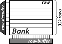
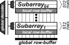
Observation 1. A modern DRAM bank is not implemented as a monolithic component equipped with only a single row buffer. Implementing a DRAM bank in such a way requires very long internal wires (called bitlines) to connect the row buffer to all the rows in the bank, which can significantly increase the access latency. Instead, as Figure 1b shows, a bank consists of multiple subarrays, each with its own local row buffer. Subarrays within a bank share two important global structures: i) a global row address decoder, and ii) a global row buffer.

Observation 2. The latency of a bank access predominantly consists of three major components: i) loading a row into the local row buffer (activation), ii) accessing the data from the local row buffer (read or write), and iii) clearing the local row buffer (precharging) [76, 38, 37, 14, 66, 77, 78]. In existing DRAM banks, all three operations must be completed for one request before serving another request to a different row, even if the two rows reside in different subarrays. However, this does not need to be the case for two reasons. First, activation and precharging are mostly local to each subarray, which enables the opportunity to overlap these operations when they are to different subarrays. Second, if we reduce the sharing of the global structures among subarrays, we can parallelize the concurrent activation of different subarrays. Doing so would allow us to exploit the existence of multiple local row buffers across the subarrays, enabling more than just a single row to be cached for each bank and thereby increasing the row buffer hit rate.
2 Subarray-Level Parallelism
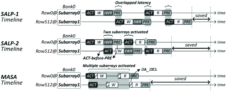
Subarray-Oblivious Baseline. Let us consider the baseline example shown in Figure 2, which presents a timeline of four memory requests being served at the same bank in a subarray-oblivious manner. This example highlights the three key problems that we discussed in Section 1. First, requests are completely serialized, even though they are to different subarrays. Second, although the write-recovery penalty is local to a subarray, it delays a subsequent request to a different subarray. Third, a request to one subarray unnecessarily evicts (i.e., precharges) the other subarray’s local row buffer, which must be reloaded (i.e., activated) when a future request accesses the evicted row. In this section, we describe how SALP-1, SALP-2 and MASA can take an advantage of the DRAM bank organization to enable parallel DRAM operations in a cost-effective manner.
2.1 SALP-1: Subarray-Level-Parallelism-1
We observe that precharging and activation are mostly local to a subarray. Based on this observation, we propose SALP-1, which overlaps the precharging of one subarray with the activation of another subarray. In contrast, existing systems always serialize precharging and activation to the same bank, conservatively provisioning for when they are to the same subarray. SALP-1 requires no modifications to existing DRAM structure. It only requires reinterpretation of an existing timing constraint (tRP) and, potentially, the addition of a new timing constraint (which we describe in Section 5.1 of our ISCA 2012 paper [66]). Figure 3 (top) shows the timeline of the same four requests from Figure 2 when we use SALP-1 instead of our Baseline. As the timeline shows, overlapping the precharge operation reduces the overall time needed to complete the four requests.
2.2 SALP-2: Subarray-Level-Parallelism-2
While SALP-1 pipelines the precharging and activation of different subarrays, the relative ordering between the two commands is still preserved. This is because existing DRAM banks do not allow two subarrays to be activated at the same time. As a result, the write-recovery latency of an activated subarray delays not only a PRECHARGE to itself, but also a subsequent ACTIVATE to another subarray. Based on the observation that the write-recovery latency is also local to a subarray, we propose SALP-2. SALP-2 issues the ACTIVATE to another subarray before the PRECHARGE to the currently-activated subarray. As a result, SALP-2 can overlap the write recovery of the currently-activated subarray with the activation of another subarray, further reducing the service time compared to SALP-1 (as shown in the middle timeline of Figure 3).
However, as highlighted in the figure, SALP-2 requires two subarrays to remain activated at the same time. This is not possible in existing DRAM banks as the global row-address latch, which determines the wordline in the bank that is raised, is shared by all of the subarrays. Section 5.2 of our ISCA 2012 paper [66] discusses how to enable SALP-2 by eliminating this sharing. The key idea is to push the global address latch to each subarray, thereby creating local address latches, one per subarray.
2.3 MASA: Multitude of Activated Subarrays
Although SALP-2 allows two subarrays within a bank to be activated, it requires the controller to precharge one of them before issuing a column command (e.g., READ) to the bank. This is because when a bank receives a column command, all activated subarrays in the bank will connect their local row buffers to the global bitlines. If more than one subarray is activated, this will result in a short circuit. As a result, SALP-2 cannot allow multiple subarrays to concurrently remain activated and serve column commands.
To solve this, we propose MASA, whose key idea is to allow multiple subarrays to be activated at the same time, while allowing the memory controller to designate exactly one of the activated subarrays to drive the global bitlines during the next column command. MASA has two advantages over SALP-2. First, MASA overlaps the activation of different subarrays within a bank. Just before issuing a column command to any of the activated subarrays, the memory controller designates one particular subarray whose row buffer should serve the column command. Second, MASA eliminates extra ACTIVATEs to the same row, thereby mitigating row buffer thrashing. This is because the local row buffers of multiple subarrays can remain activated at the same time without experiencing collisions on the global bitlines. As a result, MASA further improves performance compared to SALP-2, as shown in the bottom timeline of Figure 3.
MASA: Overhead. To designate one of the multiple activated subarrays, the controller needs a new command, SA_SEL (subarray-select). In addition to the changes required by SALP-2, MASA requires a single-bit latch per subarray to denote whether a subarray is designated or not. According to our detailed circuit-level analysis, MASA increases the DRAM die-size by only 0.15% (due to extra latches) and the static power consumption by only 1% (each additional activated subarray consumes 0.56mW). Also, the memory controller needs less than 256 bytes to track the status of subarrays across all DRAM banks. We discuss a detailed implementation of MASA, along with its overhead, in Section 5.3 of our ISCA 2012 paper [66].
3 Experimental Methodology
We evaluate our three mechanisms for subarray-level parallelism using Ramulator [62, 124], an open-source cycle-accurate DRAM simulator that we developed which accurately models DRAM subarrays. We use Ramulator as part of a cycle-level in-house x86 multi-core simulator, whose front-end is based on Pin [85]. We calculate DRAM dynamic energy consumption by associating an energy cost with each DRAM command, derived using Micron’s DDR3 DRAM tool [93], Rambus’ DRAM power model [123], and previously published data [150].
We evaluate SALP-1, SALP-2, and MASA on a wide variety of workloads [146, 39, 89, 41] and system configurations [46, 45, 143, 134]. The results shown in Section 4 are based on the conservative assumption that a DRAM bank exposes only 8 subarrays to be exploited by our subarray-level parallelism mechanisms, whereas in practice the number of subarrays in current DRAM banks is typically much higher (64). Section 9.2 of our ISCA 2012 paper [66] shows that the performance improvement of our three mechanisms over a subarray-oblivious baseline increases with a greater number of subarrays.
For our full methodology, we refer the reader to Section 8 of our ISCA 2012 paper [66].
4 Evaluation
Figure 4 shows the performance improvement of SALP-1, SALP-2, and MASA on a system with 8 subarrays-per-bank over a subarray-oblivious baseline. The figure also shows the performance improvement of an “Ideal” scheme which is the subarray-oblivious baseline with 8 times as many banks (this represents a system where all subarrays are fully independent). The benchmarks are sorted along the x-axis by increasing memory intensity. We make two observations from the figure. First, SALP-1, SALP-2, and MASA consistently perform better than the baseline for all benchmarks. On average, they improve the average performance by 6.6%, 13.4%, and 16.7%, respectively. Second, MASA captures most of the benefits of “Ideal,” which improves performance by 19.6% compared to baseline.
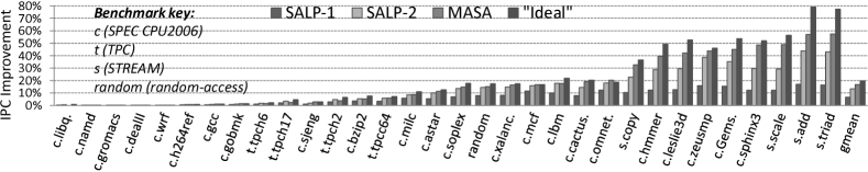
The difference in performance improvement across benchmarks can be explained by a combination of three factors related to the benchmarks’ individual memory access behavior. First, subarray-level parallelism in general is most beneficial for memory-intensive benchmarks that frequently access memory (e.g., the benchmarks located towards the right of Figure 4). By increasing the memory throughput for such applications, subarray-level parallelism significantly alleviates their memory bottleneck. The average memory intensity of the applications that gain 5% performance with SALP-1 is 18.4 MPKI (last-level cache misses per kilo-instruction), compared to 1.14 MPKI for the other applications.
Second, the advantage of SALP-2 is large for applications that are write-intensive (i.e., those with the most write misses per kilo-instruction, or WMPKI). For such applications, SALP-2 can overlap the long write-recovery latency with the activation of a subsequent access. In Figure 4, the three applications that improve more than 38% with SALP-2 are among both the most memory-intensive (25 MPKI) and the most write-intensive (15 WMPKI).
Third, MASA is beneficial for applications that experience frequent bank conflicts. For such applications, MASA parallelizes accesses to different subarrays by concurrently activating multiple subarrays (ACTIVATE) and allowing the application to switch between the activated subarrays at low cost (SA_SEL). Therefore, the subarray-level parallelism offered by MASA can be gauged by the SA_SEL-to-ACTIVATE ratio. For the nine applications that benefit more than 30% from MASA, on average, one SA_SEL was issued for every two ACTIVATEs, compared to one-in-seventeen for all other applications. For a few benchmarks, MASA performs slightly worse than SALP-2. This is because the baseline scheduling algorithm used with MASA tries to overlap as many ACTIVATEs as possible, and in the process inadvertently delays the column command of the most critical request. This delay to the most critical request slightly degrades performance for these benchmarks.222For one benchmark, MASA performs slightly better than “Ideal” due to interactions with the scheduler.
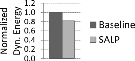
Energy Efficiency. We focus on the energy efficiency of MASA. MASA utilizes multiple local row buffers across subarrays and increases the chance that an access will hit in a local row buffer. Specifically, MASA increases the row buffer hit rate by an average of 12.8% across 32 benchmarks. A row buffer hit not only has a lower access latency, but also consumes less energy, since it does not require the power-hungry operations of activation and, to a lesser degree, precharging. Consequently, MASA reduces the dynamic energy consumption by 18.6% as shown in Figure 5.
Our ISCA 2012 paper [66] provides a detailed evaluation of SALP-1, SALP-2, and MASA, including:
-
•
Sensitivity studies to (1) the number of channels (1–8), ranks (1–8), banks (8–64), and subarrays per bank (1–128) in the memory system; (2) the mapping policy (row-/line-interleaved); and (3) an open-row or closed-policy (Sections 9.2 and 9.3 of [66]).
-
•
Multi-core results using an application-aware memory scheduling algorithm, where we show significant performance improvements (Section 9.3 of [66]).
-
•
An analysis of the power and area overhead at both the DRAM chip and the memory controller (Section 6 of [66]).
5 Related Work
To our knowledge, our ISCA 2012 paper [66] is the first to exploit the existence of subarrays within a DRAM bank and enable their parallel operation in a cost-effective manner. We propose three schemes that exploit the existence of subarrays within DRAM banks to mitigate the negative effects of bank conflicts. Related works propose increasing the performance and energy-efficiency of DRAM through approaches such as DRAM module reorganization, changes to DRAM chip design, and memory controller optimizations. We briefly discuss these works here.
DRAM Module Reorganization. Several prior works [151, 3, 164, 4] partition a DRAM rank and the DRAM data bus into multiple rank subsets, each of which can be operated independently. While these techniques increase parallelism, they reduce the width of the data bus of each rank subset, leading to longer latencies to transfer a 64 byte cache line. Furthermore, having many rank subsets requires a correspondingly large number of DRAM chips to compose a DRAM rank, an assumption that does not hold in mobile DRAM systems where a rank may consist of as few as two chips [95]. Unlike these works, our mechanisms increase memory-level parallelism [100, 108, 105, 101, 107, 120, 72] without increasing memory latency or the number of DRAM chips.
Changes to DRAM Design. Cached DRAM organizations, which have been widely proposed [25, 36, 40, 44, 56, 110, 125, 152, 161], augment DRAM chips with an additional SRAM cache that can store recently accessed data in order to reduce memory access latency. However, these proposals increase the chip area and design complexity of DRAM designs. Furthermore, cached DRAM provides parallelism only when accesses hit in the SRAM cache, while serializing cache misses that access the same DRAM bank. Our schemes parallelize DRAM bank accesses while incurring significantly lower area and logic complexity.
Fujitsu’s FCRAM [126] and Micron’s RLDRAM [57] propose to implement shorter local bitlines (i.e., fewer cells per bitline) that are quickly drivable due to their lower capacitance in order to reduce DRAM latency. However, this significantly increases the DRAM die size (30-40% for FCRAM, 40-80% for RLDRAM) because the large area of sense-amplifiers is amortized over a smaller number of cells. Hybrid memory systems can reduce the die size overhead by using a small amount of FCRAM [126] or RLDRAM [57] in conjunction with conventional DRAM and managing which subset of the data resides in FCRAM/RLDRAM at any given time to lower the latency of memory accesses.
A patent by Qimonda [113] proposes the high-level notion of separately addressable sub-banks, but lacks concrete mechanisms for exploiting the independence between sub-banks. Yamauchi et al. propose the Hierarchical Multi-Bank (HMB) [154], which parallelizes accesses to different subarrays in a fine-grained manner. However, this scheme adds complex logic to all subarrays.
Udipi et al. [147] propose two techniques (SBA and SSA) to lower DRAM power. In SBA, global wordlines are segmented and controlled separately so that tiles in the horizontal direction are not activated in lockstep, but selectively. However, this increases DRAM chip area by 12-100% [147]. SSA combines SBA with chip-granularity rank-subsetting to achieve even higher energy savings. Both SBA and SSA increase DRAM latency, more significantly so for SSA (due to rank-subsetting).
When transitioning from serving a write request to serving a read request, and vice versa [18, 73, 137], a DRAM chip experiences bubbles in the data bus, called the bus-turnaround penalty (tWTR and tRTW). During the bus turnaround penalty, Chatterjee et al. [18] propose to internally “prefetch” data for subsequent read requests into extra registers that are added to the DRAM chip.
Other works propose new DRAM designs that are capable of reducing memory latency of conventional DRAM [14, 16, 77, 78, 76, 75, 79, 94, 126, 36, 40, 44, 56, 135, 86, 19, 118, 133, 112, 164, 151, 3, 4] as well as non-volatile memory [90, 68, 91, 155, 122, 121, 69, 71, 70]. Previous works on bulk data transfer [33, 34, 53, 13, 158, 127, 47, 163, 51, 129, 84, 16] and in-memory computation [1, 2, 26, 28, 35, 116, 128, 88, 23, 131, 130, 42, 43, 12, 136, 27, 32, 55, 67, 114, 144, 157, 5, 9, 29, 119, 117, 132, 30, 60, 11] can be used improve DRAM bandwidth utilization and lower the number of costly data movements between CPU cores and DRAM. All these works can benefit from SALP as the underlying memory substrate.
Memory Controller Optimizations. To reduce bank conflicts and increase row buffer locality, Zhang et al. [160] propose to randomize the bank address of memory requests by XOR hashing. Sudan et al. [142] propose to improve row buffer locality by placing frequently-referenced data from different rows together in the same row buffer. Both proposals can be combined with our mechanisms to further improve parallelism and row buffer locality.
Prior works propose memory scheduling algorithms for CPUs (e.g., [24, 64, 65, 99, 106, 107, 111, 139, 141, 48, 98, 74, 72, 137, 73, 97, 31, 153, 82, 138, 140, 96, 162, 58, 59]), GPUs (e.g., [7, 50, 20, 8, 52]), and other systems (e.g., [149, 148, 162]) that prioritize certain favorable requests in the memory controller to improve system performance and/or fairness. Subarrays expose more parallelism to the memory controller, increasing the controller’s flexibility to schedule requests. Our subarray-level parallelism mechanisms can be combined with many of these schedulers to provide increased performance benefits. Enabling higher benefit from SALP by designing SALP-aware memory scheduling algorithms is a promising open research topic.
6 Significance and Long-Term Impact
We believe SALP will have long-term impact because: i) it tackles a critical problem, bank conflicts and memory parallelism, whose importance will increase in the future; and ii) the memory substrate it provides can further be leveraged to enable other novel optimizations in the memory subsystem. In fact, as Section 6.2 shows, there has been a significant amount of work that built upon our ISCA 2012 paper in the past six years.
6.1 Trends and Opportunities in Favor of SALP
Worsening Bank Conflicts. Future many-core systems with large numbers of cores and accelerators (e.g., bandwidth-hungry GPUs) will exert increasingly larger amount of pressure on the memory subsystem. On the other hand, naively adding more DRAM banks is difficult without incurring high costs, high energy or reduced performance. Therefore, as more and more memory requests contend to access a limited er of banks, bank conflicts will occur with increasing likelihood and severity. SALP is a cost-effective mechanism to alleviate the bank conflict problem by exploiting the existing subarrays in DRAM at low cost.
Challenges in DRAM Scaling. DRAM process scaling is becoming more difficult due to increased manufacturing complexity/cost and reduced cell reliability [63, 102, 104, 109, 103, 6, 49, 54]. As a result, it is critical to examine alternative ways of improving memory performance while still maintaining low cost. SALP is a new cost-effective DRAM design whose advantages are mostly orthogonal to the advantages of DRAM process scaling. Therefore, SALP can further improve the performance and the energy-efficiency of future DRAM. In fact, a recent industry proposal to enhance the DDR standard incorporates one of our SALP mechanisms [54]. This work by Samsung and Intel quantitatively shows that SALP is an effective mechanism to tolerate increasing write latencies in DRAM, corroborating the results in our ISCA 2012 paper on SALP-2.
A Building Block for New Optimizations. SALP enables new DRAM optimizations that were not possible before. We discuss three potential examples. First, exploiting subarray-level parallelism can potentially mitigate DRAM unavailability during refresh by parallelizing refreshes in one subarray with accesses to another subarray within the same bank. Work by Chang et al. [15], which builds on our ISCA 2012 paper, shows that such parallelization can eliminate most of the performance overhead of refresh. Second, subarrays provide an additional degree of freedom in mapping the physical address space onto different levels of the DRAM hierarchy (channels, ranks, banks, subarrays, rows, columns). Thus, they enable more flexibility in performance and energy optimization via data mapping. Third, DRAM can be divided among different applications (to provide quality-of-service) at the finer-grained partitions of subarrays that are less vulnerable to capacity and bandwidth fragmentation. As we discuss, some research has explored these approaches (also see Section 6.2). We expect even more future research will tap into these and other opportunities that can use our proposed SALP substrate as a building block for other optimizations.
Widely Applicable Substrate. SALP is a general-purpose substrate that is also applicable to embedded DRAM (eDRAM) [10] and 3D die-stacked DRAM (3D-DRAM), both of which consist of subarrays [83, 75]. For example, eDRAM is known to be vulnerable to the write-recovery penalty [22], since it is typically used as the last-level cache and thus exposed to higher amounts of write traffic. SALP can increase the availability of eDRAM by hiding the write-recovery penalty. In addition, SALP may be applied to future emerging memory technologies as long as their banks are organized hierarchically [69, 92], similar to how a DRAM bank consists of subarrays.
New Research Opportunities. SALP creates new opportunities for exploiting and enhancing the parallelism and the locality of the memory subsystem.
-
•
Enhancing Memory-Level Parallelism. To tolerate the long latency of DRAM, computer architects often design mechanisms that perform multiple memory requests in a concurrent manner [145, 100, 108, 105, 101, 107, 120, 72]. Such efforts may become ineffective when requests access the same DRAM bank and, as a consequence, are not actually served in parallel [107]. SALP, on the other hand, parallelizes requests to different subarrays within the same bank. In this regard, we believe SALP not only enhances previous approaches to memory-level parallelism, but also creates opportunities for developing new techniques that preserve memory-level parallelism in a subarray-aware manner.
-
•
Enhancing Memory Locality. Memory access patterns that exhibit high locality benefit greatly from a DRAM bank’s row buffer where the last accessed row is cached (4–8kB). While a DRAM bank has multiple row buffers across multiple subarrays, an existing DRAM system exposes only one row buffer at a time in a bank and, as a result, is prone to row buffer thrashing. In contrast, SALP allows a DRAM bank to utilize multiple row buffers concurrently. This enables the opportunity for new techniques that can take advantage of the multiple row buffers, whether they be for streaming/strided accesses (demand or prefetch), vector processing, or GPUs.
6.2 Works Building on SALP
The introduction of the notion of subarrays and their microarchitecture has enabled the use of the subarrays in many works. These include RowClone [129], TL-DRAM [78], DSARP [15], DIVA-DRAM [76], LISA [16], ChargeCache [37], Multiple Clone Row DRAM [21], Ambit [130, 128], ERUCA [87], and other works on improving DRAM [159, 84, 156, 135]. Some of these works exploit subarray level parallelism, e.g., DSARP [15] reduces the overhead of a DRAM refresh by decoupling independent subarrays from the subarray that is being refreshed. This decoupling allows DRAM to service memory accesses while a subarray is being refreshed. Others make changes to subarrays to improve an aspect, e.g., TL-DRAM [78] creates two different latency regions in a subarray to improve DRAM latency at low cost.
7 Conclusion
Our ISCA 2012 paper [66] introduces three new mechanisms that exploit the existence of subarrays within a DRAM bank to mitigate the performance impact of bank conflicts. Our mechanisms are built on the key observation that subarrays within a DRAM bank operate largely independently and have their own row buffers. Hence, the latencies of accesses to different subarrays within the same bank can potentially be overlapped to a large degree. Our three mechanisms take advantage of this fact and progressively increase the independence of operation of subarrays by making small modifications to the DRAM chip. Our most sophisticated scheme, MASA, enables i) multiple subarrays to be accessed in parallel, and ii) multiple row buffers to remain activated at the same time in different subarrays, thereby improving both memory-level parallelism and row buffer locality. We show that our schemes significantly improve system performance on both single-core and multi-core systems on a variety of workloads while incurring little (0.15%) or no area overhead in the DRAM chip. Our techniques can also improve memory energy efficiency.
We conclude that exploiting subarray-level parallelism in a DRAM bank can be a promising and cost-effective method for overcoming the negative effects of DRAM bank conflicts, without paying the large cost of increasing the number of banks in the DRAM system. Significant recent work has built upon our ISCA 2012 paper, and we expect many other new works can exploit the new substrate we have enabled to achieve even bigger goals and higher benefits.
Acknowledgments
We thank Rachata Ausavarungnirun and Saugata Ghose for their dedicated effort in the preparation of this article. Many thanks to Uksong Kang, Hak-soo Yu, Churoo Park, Jung-Bae Lee, and Joo Sun Choi from Samsung for their helpful comments. We thank the anonymous reviewers for their feedback. We gratefully acknowledge members of the SAFARI group for feedback and for the stimulating intellectual environment they provide. We acknowledge the generous support of AMD, Intel, Oracle, and Samsung. This research was also partially supported by grants from NSF (CAREER Award CCF- 0953246), GSRC, and Intel ARO Memory Hierarchy Program.
References
- [1] J. Ahn, S. Hong, S. Yoo, O. Mutlu, and K. Choi, “A Scalable Processing-in-memory Accelerator for Parallel Graph Processing,” in ISCA, 2015.
- [2] J. Ahn, S. Yoo, O. Mutlu, and K. Choi, “PIM-enabled Instructions: A Low-overhead, Locality-aware Processing-in-memory Architecture,” in ISCA, 2015.
- [3] J. H. Ahn, J. Leverich, R. Schreiber, and N. P. Jouppi, “Multicore DIMM: an Energy Efficient Memory Module with Independently Controlled DRAMs,” IEEE CAL, 2009.
- [4] J. H. Ahn, N. P. Jouppi, C. Kozyrakis, J. Leverich, and R. S. Schreiber, “Improving System Energy Efficiency with Memory Rank Subsetting,” TACO, 2012.
- [5] B. Akin, F. Franchetti, and J. C. Hoe, “Data Reorganization in Memory Using 3D-stacked DRAM,” in ISCA, 2015.
- [6] G. Atwood, “Current and Emerging Memory Technology Landscape (Micron),” in Flash Memory Summit, 2011.
- [7] R. Ausavarungnirun, K. K. Chang, L. Subramanian, G. Loh, and O. Mutlu, “Staged Memory Scheduling: Achieving High Performance and Scalability in Heterogeneous Systems,” in ISCA, 2012.
- [8] R. Ausavarungnirun, S. Ghose, O. Kayıran, G. H. Loh, C. R. Das, M. T. Kandemir, and O. Mutlu, “Exploiting Inter-Warp Heterogeneity to Improve GPGPU Performance,” in PACT, 2015.
- [9] O. O. Babarinsa and S. Idreos, “JAFAR: Near-Data Processing for Databases,” in SIGMOD, 2015.
- [10] J. Barth, D. Plass, E. Nelson, C. Hwang, G. Fredeman, M. Sperling, A. Mathews, T. Kirihata, W. R. Reohr, K. Nair, and N. Caon, “A 45 nm SOI Embedded DRAM Macro for the POWER Processor 32 MByte On-Chip L3 Cache,” JSSC, 2011.
- [11] A. Boroumand, S. Ghose, Y. Kim, R. Ausavarungnirun, E. Shiu, R. Thakur, D. Kim, A. Kuusela, A. Knies, P. Ranganathan, and O. Mutlu, “Google Workloads for Consumer Devices: Mitigating Data Movement Bottlenecks,” in ASPLOS, 2018.
- [12] A. Boroumand, S. Ghose, B. Lucia, K. Hsieh, K. Malladi, H. Zheng, and O. Mutlu, “LazyPIM: An Efficient Cache Coherence Mechanism for Processing-in-Memory,” IEEE CAL, 2016.
- [13] J. Carter, W. Hsieh, L. Stoller, M. Swanson, L. Zhang, E. Brunvand, A. Davis, C.-C. Kuo, R. Kuramkote, M. Parker, L. Schaelicke, and T. Tateyama, “Impulse: Building a Smarter Memory Controller,” in HPCA, 1999.
- [14] K. K. Chang, A. Kashyap, H. Hassan, S. Ghose, K. Hsieh, D. Lee, T. Li, G. Pekhimenko, S. Khan, and O. Mutlu, “Understanding Latency Variation in Modern DRAM Chips: Experimental Characterization, Analysis, and Optimization,” in SIGMETRICS, 2016.
- [15] K. K. Chang, D. Lee, Z. Chishti, A. Alameldeen, C. Wilkerson, Y. Kim, and O. Mutlu, “Improving DRAM Performance by Parallelizing Refreshes with Accesses ,” in HPCA, 2014.
- [16] K. K. Chang, P. J. Nair, D. Lee, S. Ghose, M. K. Qureshi, and O. Mutlu, “Low-Cost Inter-Linked Subarrays (LISA): Enabling Fast Inter-Subarray Data Movement in DRAM,” in HPCA, 2016.
- [17] K. K. Chang, A. G. Yaglikci, S. Ghose, A. Agrawal, N. Chatterjee, A. Kashyap, D. Lee, M. O’Connor, H. Hassan, and O. Mutlu, “Understanding Reduced-Voltage Operation in Modern DRAM Devices: Experimental Characterization, Analysis, and Mechanisms,” in SIGMETRICS, 2017.
- [18] N. Chatterjee et al., “Staged reads: Mitigating the impact of DRAM writes on DRAM reads,” in HPCA, 2012.
- [19] N. Chatterjee, M. Shevgoor, R. Balasubramonian, A. Davis, Z. Fang, R. Illikkal, and R. Iyer, “Leveraging Heterogeneity in DRAM Main Memories to Accelerate Critical Word Access,” in MICRO, 2012.
- [20] N. Chatterjee, M. O’Connor, G. H. Loh, N. Jayasena, and R. Balasubramonian, “Managing DRAM Latency Divergence in Irregular GPGPU Applications,” in SC, 2014.
- [21] J. Choi, W. Shin, J. Jang, J. Suh, Y. Kwon, Y. Moon, and L.-S. Kim, “Multiple Clone Row DRAM: A Low Latency and Area Optimized DRAM,” in ISCA, 2015.
- [22] B. W. Curran et al., “The zEnterprise 196 System and Microprocessor,” IEEE Micro, Mar 2011.
- [23] J. Draper, J. Chame, M. Hall, C. Steele, T. Barrett, J. LaCoss, J. Granacki, J. Shin, C. Chen, C. W. Kang, I. Kim, and G. Daglikoca, “The Architecture of the DIVA Processing-in-memory Chip,” in ICS, 2002.
- [24] E. Ebrahimi, R. Miftakhutdinov, C. Fallin, C. J. Lee, J. A. Joao, O. Mutlu, and Y. N. Patt, “Parallel Application Memory Scheduling,” in MICRO, 2011.
- [25] Enhanced Memory Systems, “Enhanced SDRAM SM2604,” 2002.
- [26] A. Farmahini-Farahani, J. H. Ahn, K. Morrow, and N. S. Kim, “NDA: Near-DRAM Acceleration Architecture Leveraging Commodity DRAM Devices and Standard Memory Modules,” in HPCA, 2015.
- [27] B. B. Fraguela, J. Renau, P. Feautrier, D. Padua, and J. Torrellas, “Programming the FlexRAM Parallel Intelligent Memory System,” in PPoPP, 2003.
- [28] M. Gao, G. Ayers, and C. Kozyrakis, “Practical Near-Data Processing for In-Memory Analytics Frameworks,” in PACT, 2015.
- [29] M. Gao and C. Kozyrakis, “HRL: Efficient and Flexible Reconfigurable Logic for Near-Data Processing,” in HPCA, 2016.
- [30] S. Ghose, K. Hsieh, A. Boroumand, R. Ausavarungnirun, and O. Mutlu, “The Processing-in-Memory Paradigm: Mechanisms to Enable Adoption,” arXiv [cs.AR], 2018.
- [31] S. Ghose, H. Lee, and J. F. Martínez, “Improving Memory Scheduling via Processor-side Load Criticality Information,” in ISCA, 2013.
- [32] M. Gokhale, B. Holmes, and K. Iobst, “Processing in Memory: the Terasys Massively Parallel PIM Array,” Computer, 1995.
- [33] M. Gschwind, “Chip Multiprocessing and the Cell Broadband Engine,” in CF, 2006.
- [34] J. Gummaraju, M. Erez, J. Coburn, M. Rosenblum, and W. J. Dally, “Architectural Support for the Stream Execution Model on General-Purpose Processors,” in PACT, 2007.
- [35] Q. Guo, N. Alachiotis, B. Akin, F. Sadi, G. Xu, T.-M. Low, L. Pileggi, J. C. Hoe, and F. Franchetti, “3D-Stacked Memory-Side Acceleration: Accelerator and System Design,” in WoNDP, 2014.
- [36] C. A. Hart, “CDRAM in a Unified Memory Architecture,” in Compcon, 1994.
- [37] H. Hassan, G. Pekhimenko, N. Vijaykumar, V. Seshadri, D. Lee, O. Ergin, and O. Mutlu, “ChargeCache: Reducing DRAM Latency by Exploiting Row Access Locality,” in HPCA, 2016.
- [38] H. Hassan, N. Vijaykumar, S. Khan, S. Ghose, K. K. Chang, G. Pekhimenko, D. Lee, O. Ergin, and O. Mutlu, “SoftMC: A Flexible and Practical Open-source Infrastructure for Enabling Experimental DRAM Studies,” in HPCA, 2017.
- [39] J. L. Henning, “SPEC CPU2006 benchmark descriptions,” CAN, 2006.
- [40] H. Hidaka, Y. Matsuda, M. Asakura, and K. Fujishima, “The Cache DRAM Architecture,” IEEE Micro, 1990.
- [41] HPC Challenge, “GUPS,” http://icl.cs.utk.edu/projectsfiles/hpcc/RandomAccess/.
- [42] K. Hsieh, S. Khan, N. Vijaykumar, K. K. Chang, A. Boroumand, S. Ghose, and O. Mutlu, “Accelerating Pointer Chasing in 3D-stacked Memory: Challenges, Mechanisms, Evaluation,” in ICCD, 2016.
- [43] K. Hsieh, E. Ebrahimi, G. Kim, N. Chatterjee, M. O’Connor, N. Vijaykumar, O. Mutlu, and S. W. Keckler, “Transparent Offloading and Mapping (TOM): Enabling Programmer-Transparent Near-Data Processing in GPU Systems,” in ISCA, 2016.
- [44] W.-C. Hsu and J. E. Smith, “Performance of Cached DRAM Organizations in Vector Supercomputers,” in ISCA, 1993.
- [45] Intel, “2nd Gen. Intel Core Processor Family Desktop Datasheet,” 2011.
- [46] Intel, “Intel Core Desktop Processor Series Datasheet,” 2011.
- [47] Intel Corp., “Intel®I/O Acceleration Technology,” http://www.intel.com/content/www/us/en/wireless-network/accel-technology.html.
- [48] E. Ipek, O. Mutlu, J. F. Martínez, and R. Caruana, “Self-optimizing memory controllers: A reinforcement learning approach,” in ISCA, 2008.
- [49] ITRS, “International Technology Roadmap for Semiconductors,” 2011.
- [50] M. K. Jeong, M. Erez, C. Sudanthi, and N. Paver, “A QoS-Aware Memory Controller for Dynamically Balancing GPU and CPU Bandwidth Use in an MPSoC,” in DAC, 2012.
- [51] X. Jiang, Y. Solihin, L. Zhao, and R. Iyer, “Architecture Support for Improving Bulk Memory Copying and Initialization Performance,” in PACT, 2009.
- [52] A. Jog, O. Kayiran, A. Pattnaik, M. T. Kandemir, O. Mutlu, R. Iyer, and C. R. Das, “Exploiting Core Criticality for Enhanced GPU Performance,” in SIGMETRICS, 2016.
- [53] J. A. Kahle, M. N. Day, H. P. Hofstee, C. R. Johns, T. R. Maeurer, and D. Shippy, “Introduction to the Cell Multiprocessor,” IBM JRD, 2005.
- [54] U. Kang, H.-S. Yu, C. Park, H. Zheng, J. Halbert, K. Bains, S. Jang, and J. Choi, “Co-Architecting Controllers and DRAM to Enhance DRAM Process Scaling,” in The Memory Forum, 2014.
- [55] Y. Kang, W. Huang, S.-M. Yoo, D. Keen, Z. Ge, V. Lam, P. Pattnaik, and J. Torrellas, “FlexRAM: Toward an Advanced Intelligent Memory System,” in ICCD, 1999.
- [56] G. Kedem and R. P. Koganti, “WCDRAM: A Fully Associative Integrated Cached-DRAM with Wide Cache Lines,” Duke Univ. Dept. of Computer Science, Tech. Rep. CS-1997-03, 1997.
- [57] B. Keeth et al., DRAM Circuit Design. Fundamental and High-Speed Topics. Wiley-IEEE Press, 2007.
- [58] H. Kim, D. de Niz, B. Andersson, M. Klein, O. Mutlu, and R. Rajkumar, “Bounding Memory Interference Delay in COTS-based Multi-core Systems,” in RTAS, 2014.
- [59] H. Kim, D. de Niz, B. Andersson, M. Klein, O. Mutlu, and R. Rajkumar, “Bounding and Reducing Memory Interference in COTS-based Multi-core Systems,” RTS, 2016.
- [60] J. S. Kim, D. Senol, H. Xin, D. Lee, S. Ghose, M. Alser, H. Hassan, O. Ergin, C. Alkan, and O. Mutlu, “GRIM-Filter: Fast Seed Location Filtering in DNA Read Mapping Using Processing-in-Memory Technologies,” BMC Genomics, 2018.
- [61] J. S. Kim, M. Patel, H. Hassan, and O. Mutlu, “The DRAM Latency PUF: Quickly Evaluating Physical Unclonable Functions by Exploiting the Latency-Reliability Tradeoff in Modern DRAM Devices,” in HPCA, 2018.
- [62] Y. Kim, W. Yang, and O. Mutlu, “Ramulator: A Fast and Extensible DRAM Simulator,” IEEE CAL, 2015.
- [63] Y. Kim, R. Daly, J. Kim, C. Fallin, J. H. Lee, D. Lee, C. Wilkerson, K. Lai, and O. Mutlu, “Flipping Bits in Memory Without Accessing Them: An Experimental Study of DRAM Disturbance Errors,” in ISCA, 2014.
- [64] Y. Kim, D. Han, O. Mutlu, and M. Harchol-Balter, “ATLAS: A Scalable and High-Performance Scheduling Algorithm for Multiple Memory Controllers,” in HPCA, 2010.
- [65] Y. Kim, M. Papamichael, O. Mutlu, and M. Harchol-Balter, “Thread Cluster Memory Scheduling: Exploiting Differences in Memory Access Behavior,” in MICRO, 2010.
- [66] Y. Kim, V. Seshadri, D. Lee, J. Liu, and O. Mutlu, “A Case for Exploiting Subarray-Level Parallelism (SALP) in DRAM,” in ISCA, 2012.
- [67] P. M. Kogge, “EXECUBE-A New Architecture for Scaleable MPPs,” in ICPP, 1994.
- [68] E. Kultursay, M. Kandemir, A. Sivasubramaniam, and O. Mutlu, “Evaluating STT-RAM as an energy-efficient main memory alternative,” in ISPASS, 2013.
- [69] B. C. Lee, E. Ipek, O. Mutlu, and D. Burger, “Architecting Phase Change Memory as a Scalable DRAM Alternative,” in ISCA, 2009.
- [70] B. C. Lee, E. Ipek, O. Mutlu, and D. Burger, “Phase Change Memory Architecture and the Quest for Scalability,” CACM, 2010.
- [71] B. C. Lee, P. Zhou, J. Yang, Y. Zhang, B. Zhao, E. Ipek, O. Mutlu, and D. Burger, “Phase-Change Technology and the Future of Main Memory,” IEEE Micro, 2010.
- [72] C. J. Lee, V. Narasiman, O. Mutlu, and Y. N. Patt, “Improving Memory Bank-Level Parallelism in the Presence of Prefetching,” in MICRO, 2009.
- [73] C. J. Lee, E. Ebrahimi, V. Narasiman, O. Mutlu, and Y. N. Patt, “DRAM-Aware Last-Level Cache Writeback: Reducing Write-Caused Interference in Memory Systems,” Univ. of Texas at Austin, High Performance Systems Group, Tech. Rep. TR-HPS-2010-002, 2010.
- [74] C. J. Lee, O. Mutlu, V. Narasiman, and Y. N. Patt, “Prefetch-aware DRAM Controllers,” in MICRO, 2008.
- [75] D. Lee, S. Ghose, G. Pekhimenko, S. Khan, and O. Mutlu, “Simultaneous Multi-layer Access: Improving 3D-stacked Memory Bandwidth at Low Cost,” TACO, 2016.
- [76] D. Lee, S. Khan, L. Subramanian, S. Ghose, R. Ausavarungnirun, G. Pekhimenko, V. Seshadri, and O. Mutlu, “Design-Induced Latency Variation in Modern DRAM Chips: Characterization, Analysis, and Latency Reduction Mechanisms,” in SIGMETRICS, 2017.
- [77] D. Lee, Y. Kim, G. Pekhimenko, S. Khan, V. Seshadri, K. K. Chang, and O. Mutlu, “Adaptive-latency DRAM: Optimizing DRAM Timing for the Common-case,” in HPCA, 2015.
- [78] D. Lee, Y. Kim, V. Seshadri, J. Liu, L. Subramanian, and O. Mutlu, “Tiered-latency DRAM: A Low Latency and Low Cost DRAM Architecture,” in HPCA, 2013.
- [79] D. Lee, L. Subramanian, R. Ausavarungnirun, J. Choi, and O. Mutlu, “Decoupled Direct Memory Access: Isolating CPU and IO Traffic by Leveraging a Dual-Data-Port DRAM,” in PACT, 2015.
- [80] J. Liu, B. Jaiyen, Y. Kim, C. Wilkerson, and O. Mutlu, “An Experimental Study of Data Retention Behavior in Modern DRAM Devices: Implications for Retention Time Profiling Mechanisms,” in ISCA, 2013.
- [81] J. Liu, B. Jaiyen, R. Veras, and O. Mutlu, “RAIDR: Retention-Aware Intelligent DRAM Refresh,” in ISCA, 2012.
- [82] W. Liu, P. Huang, T. Kun, T. Lu, K. Zhou, C. Li, and X. He, “LAMS: A Latency-aware Memory Scheduling Policy for Modern DRAM Systems,” in IPCCC, 2016.
- [83] G. H. Loh, “3D-stacked Memory Architectures for Multi-core Processors,” in ISCA, 2008.
- [84] S.-L. Lu, Y.-C. Lin, and C.-L. Yang, “Improving DRAM Latency with Dynamic Asymmetric Subarray,” in MICRO, 2015.
- [85] C.-K. Luk, R. Cohn, R. Muth, H. Patil, A. Klauser, G. Lowney, S. Wallace, V. J. Reddi, and K. Hazelwood, “Pin: building customized program analysis tools with dynamic instrumentation,” in PLDI, 2005.
- [86] Y. Luo, S. Govindan, B. Sharma, M. Santaniello, J. Meza, A. Kansal, J. Liu, B. Khessib, K. Vaid, and O. Mutlu, “Characterizing Application Memory Error Vulnerability to Optimize Datacenter Cost via Heterogeneous-Reliability Memory,” in DSN, 2014.
- [87] S. Lym, H. Ha, Y. Kwon, C. Chang, J. Kim, and M. Erez, “ERUCA: Efficient DRAM Resource Utilization and Resource Conflict Avoidance for Memory System Parallelism,” in HPCA, 2018.
- [88] K. Mai, T. Paaske, N. Jayasena, R. Ho, W. J. Dally, and M. Horowitz, “Smart Memories: A Modular Reconfigurable Architecture,” in ISCA, 2000.
- [89] J. D. McCalpin, “STREAM Benchmark,” http://www.streambench.org/.
- [90] J. Meza, Y. Luo, S. Khan, J. Zhao, Y. Xie, and O. Mutlu, “A Case for Efficient Hardware/Software Cooperative Management of Storage and Memory,” in WEED, 2013.
- [91] J. Meza, J. Chang, H. Yoon, O. Mutlu, and P. Ranganathan, “Enabling Efficient and Scalable Hybrid Memories Using Fine-Granularity DRAM Cache Management,” IEEE CAL, 2012.
- [92] J. Meza, J. Li, and O. Mutlu, “A Case for Small Row Buffers in Non-volatile Main Memories,” in ICCD, 2012.
- [93] Micron Technology, Inc., “DDR3 SDRAM System-Power Calculator,” 2010.
- [94] Micron Technology, Inc., “576Mb: x18, x36 RLDRAM3,” 2011.
- [95] Micron Technology, Inc., “2Gb: x16, x32 Mobile LPDDR2 SDRAM,” 2012.
- [96] T. Moscibroda and O. Mutlu, “Memory Performance Attacks: Denial of Memory Service in Multi-core Systems,” in USENIX Security, 2007.
- [97] T. Moscibroda and O. Mutlu, “Distributed Order Scheduling and Its Application to Multi-core DRAM Controllers,” in PODC, 2008.
- [98] J. Mukundan and J. F. Martinez, “MORSE: Multi-objective Reconfigurable Self-optimizing Memory Scheduler,” in HPCA, 2012.
- [99] S. P. Muralidhara, L. Subramanian, O. Mutlu, M. Kandemir, and T. Moscibroda, “Reducing Memory Interference in Multicore Systems via Application-Aware Memory Channel Partitioning,” in MICRO, 2011.
- [100] O. Mutlu, H. Kim, and Y. N. Patt, “Address-value Delta (AVD) Prediction: Increasing the Effectiveness of Runahead Execution by Exploiting Regular Memory Allocation Patterns,” in MICRO, 2005.
- [101] O. Mutlu, J. Stark, C. Wilkerson, and Y. N. Patt, “Runahead execution: An effective alternative to large instruction windows,” IEEE Micro, 2003.
- [102] O. Mutlu, “Memory Scaling: A Systems Architecture Perspective,” IMW, 2013.
- [103] O. Mutlu, “Memory Scaling: A Systems Architecture Perspective,” in MEMCON, 2013.
- [104] O. Mutlu, “The RowHammer Problem and Other Issues We May Face as Memory Becomes Denser,” in DATE, 2017.
- [105] O. Mutlu, H. Kim, and Y. N. Patt, “Techniques for Efficient Processing in Runahead Execution Engines,” in ISCA, 2005.
- [106] O. Mutlu and T. Moscibroda, “Stall-time fair memory access scheduling for chip multiprocessors,” in MICRO, 2007.
- [107] O. Mutlu and T. Moscibroda, “Parallelism-Aware Batch Scheduling: Enhancing both Performance and Fairness of Shared DRAM Systems,” in ISCA, 2008.
- [108] O. Mutlu, J. Stark, C. Wilkerson, and Y. N. Patt, “Runahead Execution: An Alternative to Very Large Instruction Windows for Out-of-Order Processors,” in HPCA, 2003.
- [109] O. Mutlu and L. Subramanian, “Research Problems and Opportunities in Memory Systems,” SUPERFRI, 2014.
- [110] NEC, “Virtual Channel SDRAM uPD4565421,” 1999.
- [111] K. J. Nesbit, N. Aggarwal, J. Laudon, and J. E. Smith, “Fair queuing memory systems,” in MICRO, 2006.
- [112] S. O, Y. H. Son, N. S. Kim, and J. H. Ahn, “Row-Buffer Decoupling: A Case for Low-Latency DRAM Microarchitecture,” in ISCA, 2014.
- [113] J.-H. Oh, “Semiconductor memory having a bank with sub-banks,” U.S. Patent 7,782,703, 2010.
- [114] M. Oskin, F. T. Chong, and T. Sherwood, “Active Pages: A Computation Model for Intelligent Memory,” in ISCA, 1998.
- [115] M. Patel, J. Kim, and O. Mutlu, “The Reach Profiler (REAPER): Enabling the Mitigation of DRAM Retention Failures via Profiling at Aggressive Conditions,” in ISCA, 2017.
- [116] D. Patterson, T. Anderson, N. Cardwell, R. Fromm, K. Keeton, C. Kozyrakis, R. Thomas, and K. Yelick, “A Case for Intelligent RAM,” IEEE Micro, 1997.
- [117] A. Pattnaik, X. Tang, A. Jog, O. Kayiran, A. K. Mishra, M. T. Kandemir, O. Mutlu, and C. R. Das, “Scheduling Techniques for GPU Architectures with Processing-In-Memory Capabilities,” in PACT, 2016.
- [118] S. Phadke and S. Narayanasamy, “MLP Aware Heterogeneous Memory System,” in DATE, 2011.
- [119] S. H. Pugsley, J. Jestes, H. Zhang, R. Balasubramonian, V. Srinivasan, A. Buyuktosunoglu, A. Davis, and F. Li, “NDC: Analyzing the Impact of 3D-stacked Memory+logic Devices on MapReduce Workloads,” in ISPASS, 2014.
- [120] M. K. Qureshi, D. Lynch, O. Mutlu, and Y. Patt, “A Case for MLP-Aware Cache Replacement,” in ISCA, 2006.
- [121] M. K. Qureshi, J. Karidis, M. Franceschini, V. Srinivasan, L. Lastras, and B. Abali, “Enhancing Lifetime and Security of PCM-based Main Memory with Start-gap Wear Leveling,” in MICRO, 2009.
- [122] M. K. Qureshi, V. Srinivasan, and J. A. Rivers, “Scalable High Performance Main Memory System Using Phase-change Memory Technology,” in ISCA, 2009.
- [123] Rambus, “DRAM Power Model,” 2010.
- [124] SAFARI Research Group, “Ramulator – GitHub Repository,” https://github.com/CMU-SAFARI/ramulator.
- [125] R. H. Sartore, K. J. Mobley, D. G. Carrigan, and O. F. Jones, “Enhanced DRAM with embedded registers,” U.S. Patent 5,887,272, 1999.
- [126] Y. Sato, T. Suzuki, T. Aikawa, S. Fujioka, W. Fujieda, H. Kobayashi, H. Ikeda, T. Nagasawa, A. Funyu, Y. Fuji, K. Kawasaki, M. Yamazaki, and M. Taguchi, “Fast cycle RAM (FCRAM): A 20-ns Random Row Access, Pipe-Lined Operating DRAM,” in VLSIC, 1998.
- [127] S.-Y. Seo, “Methods of Copying a Page in a Memory Device and Methods of Managing Pages in a Memory System,” U.S. Patent Application 20140185395, 2014.
- [128] V. Seshadri, K. Hsieh, A. Boroumand, D. Lee, M. Kozuch, O. Mutlu, P. Gibbons, and T. Mowry, “Fast Bulk Bitwise AND and OR in DRAM,” IEEE CAL, 2015.
- [129] V. Seshadri, Y. Kim, C. Fallin, D. Lee, R. Ausavarungnirun, G. Pekhimenko, Y. Luo, O. Mutlu, P. B. Gibbons, M. A. Kozuch, and T. C. Mowry, “RowClone: Fast and Energy-Efficient In-DRAM Bulk Data Copy and Initialization,” in ISCA, 2013.
- [130] V. Seshadri, D. Lee, T. Mullins, H. Hassan, A. Boroumand, J. Kim, M. A. Kozuch, O. Mutlu, P. B. Gibbons, and T. C. Mowry, “Ambit: In-memory Accelerator for Bulk Bitwise Operations using Commodity DRAM Technology,” in MICRO, 2017.
- [131] V. Seshadri, T. Mullins, A. Boroumand, O. Mutlu, P. B. Gibbons, M. A. Kozuch, and T. C. Mowry, “Gather-Scatter DRAM: In-DRAM Address Translation to Improve the Spatial Locality of Non-Unit Strided Accesses,” in MICRO, 2015.
- [132] V. Seshadri and O. Mutlu, “Simple Operations in Memory to Reduce Data Movement,” in Advances in Computers, Volume 106, 2017.
- [133] W. Shin, J. Yang, J. Choi, and L.-S. Kim, “NUAT: A Non-Uniform Access Time Memory Controller,” in HPCA, 2014.
- [134] B. Sinharoy, R. Kalla, W. J. Starke, H. Q. Le, R. Cargnoni, J. A. Van Norstrand, B. J. Ronchetti, J. Stuecheli, J. Leenstra, G. L. Guthrie et al., “IBM POWER7 multicore server processor,” IBM Journal Res. Dev., May. 2011.
- [135] Y. H. Son, S. O, Y. Ro, J. W. Lee, and J. H. Ahn, “Reducing Memory Access Latency with Asymmetric DRAM Bank Organizations,” in ISCA, 2013.
- [136] H. S. Stone, “A Logic-in-Memory Computer,” IEEE TC, vol. C-19, no. 1, pp. 73–78, 1970.
- [137] J. Stuecheli, D. Kaseridis, D. Daly, H. C. Hunter, and L. K. John, “The Virtual Write Queue: Coordinating DRAM and Last-level Cache Policies,” in ISCA, 2010.
- [138] L. Subramanian, D. Lee, V. Seshadri, H. Rastogi, and O. Mutlu, “BLISS: Balancing Performance, Fairness and Complexity in Memory Access Scheduling,” in IEEE TPDS, 2016.
- [139] L. Subramanian, D. Lee, V. Seshadri, H. Rastogi, and O. Mutlu, “The Blacklisting Memory Scheduler: Achieving high performance and fairness at low cost,” in ICCD, 2014.
- [140] L. Subramanian, V. Seshadri, A. Ghosh, S. Khan, and O. Mutlu, “The Application Slowdown Model: Quantifying and Controlling the Impact of Inter-application Interference at Shared Caches and Main Memory,” in MICRO, 2015.
- [141] L. Subramanian, V. Seshadri, Y. Kim, B. Jaiyen, and O. Mutlu, “MISE: Providing Performance Predictability and Improving Fairness in Shared Main Memory Systems,” in HPCA, 2013.
- [142] K. Sudan, N. Chatterjee, D. Nellans, M. Awasthi, R. Balasubramonian, and A. Davis, “Micro-pages: Increasing DRAM efficiency with locality-aware data placement,” in ASPLOS, 2010.
- [143] Sun Microsystems, “OpenSPARC T1 microarch. specification,” 2006.
- [144] Z. Sura, A. Jacob, T. Chen, B. Rosenburg, O. Sallenave, C. Bertolli, S. Antao, J. Brunheroto, Y. Park, K. O’Brien, and R. Nair, “Data Access Optimization in a Processing-in-memory System,” in CF, 2015.
- [145] R. M. Tomasulo, “An Efficient Algorithm for Exploiting Multiple Arithmetic Units,” IBM JRD, 1967.
- [146] Transaction Processing Performance Council, “,” http://www.tpc.org/.
- [147] A. N. Udipi, N. Muralimanohar, N. Chatterjee, R. Balasubramonian, A. Davis, and N. P. Jouppi, “Rethinking DRAM Design and Organization for Energy-constrained Multi-cores,” in ISCA, 2010.
- [148] H. Usui, L. Subramanian, K. K. Chang, and O. Mutlu, “SQUASH: Simple QoS-aware high-performance memory scheduler for heterogeneous systems with hardware accelerators,” arXiv:1505.07502 [cs.AR], 2015.
- [149] H. Usui, L. Subramanian, K. K. Chang, and O. Mutlu, “DASH: Deadline-Aware High-Performance Memory Scheduler for Heterogeneous Systems with Hardware Accelerators,” TACO, 2016.
- [150] T. Vogelsang, “Understanding the Energy Consumption of Dynamic Random Access Memories,” in MICRO, 2010.
- [151] F. A. Ware and C. Hampel, “Improving Power and Data Efficiency with Threaded Memory Modules,” in ICCD, 2006.
- [152] W. A. Wong and J.-L. Baer, “DRAM caching,” 1997.
- [153] D. Xiong, K. Huang, X. Jiang, and X. Yan, “Memory Access Scheduling Based on Dynamic Multilevel Priority in Shared DRAM Systems,” TACO, 2016.
- [154] T. Yamauchi, L. Hammond, and K. Olukotun, “The Hierarchical Multi-bank DRAM: A High-performance Architecture for Memory Integrated with Processors,” in Advanced Research in VLSI, 1997.
- [155] H. Yoon, J. Meza, R. Ausavarungnirun, R. Harding, and O. Mutlu, “Row Buffer Locality Aware Caching Policies for Hybrid Memories,” in ICCD, 2012.
- [156] J. Yue and Y. Zhu, “Exploiting Subarrays Inside a Bank to Improve Phase Change Memory Performance,” in DATE, 2013.
- [157] D. Zhang, N. Jayasena, A. Lyashevsky, J. L. Greathouse, L. Xu, and M. Ignatowski, “TOP-PIM: Throughput-oriented Programmable Processing in Memory,” in HPDC, 2014.
- [158] L. Zhang, Z. Fang, M. Parker, B. K. Mathew, L. Schaelicke, J. B. Carter, W. C. Hsieh, and S. A. McKee, “The Impulse Memory Controller,” IEEE TC, 2001.
- [159] T. Zhang, M. Poremba, C. Xu, G. Sun, and Y. Xie, “CREAM: A Concurrent-Refresh-Aware DRAM Memory Architecture,” in HPCA, 2014.
- [160] Z. Zhang, Z. Zhu, and X. Zhang, “A permutation-based page interleaving scheme to reduce row-buffer conflicts and exploit data locality,” in MICRO, 2000.
- [161] Z. Zhang, Z. Zhu, and X. Zhang, “Cached DRAM for ILP processor memory access latency reduction,” IEEE Micro, July 2001.
- [162] J. Zhao, O. Mutlu, and Y. Xie, “FIRM: Fair and High-Performance Memory Control for Persistent Memory Systems,” in MICRO, 2014.
- [163] L. Zhao, R. Iyer, S. Makineni, L. Bhuyan, and D. Newell, “Hardware Support for Bulk Data Movement in Server Platforms,” in ICCD, 2005.
- [164] H. Zheng, J. Lin, Z. Zhang, E. Gorbatov, H. David, and Z. Zhu, “Mini-rank: Adaptive DRAM Architecture for Improving Memory Power Efficiency,” in MICRO, 2008.