Superconducting Optoelectronic Neurons III: Synaptic Plasticity
Abstract
As a means of dynamically reconfiguring the synaptic weight of a superconducting optoelectronic loop neuron, a superconducting flux storage loop is inductively coupled to the synaptic current bias of the neuron. A standard flux memory cell is used to achieve a binary synapse, and loops capable of storing many flux quanta are used to enact multi-stable synapses. Circuits are designed to implement supervised learning wherein current pulses add or remove flux from the loop to strengthen or weaken the synaptic weight. Designs are presented for circuits with hundreds of intermediate synaptic weights between minimum and maximum strengths. Circuits for implementing unsupervised learning are modeled using two photons to strengthen and two photons to weaken the synaptic weight via Hebbian and anti-Hebbian learning rules, and techniques are proposed to control the learning rate. Implementation of short-term plasticity, homeostatic plasticity, and metaplasticity in loop neurons is discussed.
I Introduction
Information processing systems with differentiated processing, information integration, and distributed memory modeled after biological neural systems are appealing as tools for understanding neural and nonlinear dynamical systems as well as for computation in contexts requiring complex contextualization and dynamic learning. In such neural systems Dayan and Abbott (2001); Gerstner and Kistler (2002), the synaptic weights between nodes in the network are crucial memory elements that affect dynamics and computation Abbott and Regehr (2004); Buzsaki (2006); Siri et al. (2007); Hawkins and Ahmad (2016). For some applications, it is important to have a means by which a user can interface with the system to externally control the synaptic weights to implement learning algorithms Nielsen (2015). In other applications, it is desirable for the synaptic weights to dynamically update based on network activity in an unsupervised manner. It is beneficial for a hardware platform to be capable of both.
It has been proposed Shainline et al. (2017, 2018a) that combining the strengths of light for communication and superconducting electronics for efficient computation offers a route to large-scale neural systems. A circuit that transduces single-photon communication signals to integrated supercurrent has been described in Ref. Shainline et al., 2018b. In that reference, a means to modify the synaptic weight via a bias current () was identified. The present work explores circuits that dynamically control .
The circuits implemented to control should meet several criteria: 1) Transition between the minimum and maximum values of should be possible with a specified number of increments to control the learning rate; 2) The circuit should not be able to set outside of this range so that simple update rules or training algorithms do not result in excessively large synaptic weights; 3) It should be possible to cycle the value of from minimum to maximum and back repeatedly without degradation; 4) In addition to a means by which the synaptic weights can be incremented by an external supervisor, there should be a means by which correlated photon signals from the two neurons associated with a synapse can strengthen or weaken the synaptic weight depending on the relative arrival times of the signals from the two neurons; 5) Within this unsupervised mode of operation, synaptic update events should be induced by single-photon signals to fully exploit the energy efficiency of the superconducting optoelectronic hardware; 6) The transition probability between synaptic states should also be dynamically adjustable based on photonic signals to achieve metaplastic behavior. This paper explores circuit designs satisfying all these criteria.
A schematic of the neuron under consideration is shown in Fig. 1(a). Operation is as follows. Photons from afferent neurons are received by single-photon detectors (SPDs) Gol’tsman et al. (2001); Natarajan et al. (2012); Liu et al. (2013); Marsili et al. (2013); Verma et al. (2015) at a neuron’s synapses. Using Josephson junctions (JJs) Tinkham (1996); Duzer and Turner (1998); Kadin (1999), these detection events are converted into an integrated supercurrent that is stored in a superconducting loop. The amount of current added to the integration loop during a synaptic photon detection event is determined by the synaptic weight. The synaptic weight is dynamically adjusted by another circuit combining SPDs and JJs. When the integrated current from all the synapses of a given neuron reaches a threshold, an amplification cascade begins, resulting in the production of light from a waveguide-integrated LED. The photons thus produced fan out through a network of passive dielectric waveguides and arrive at the synaptic terminals of other neurons where the process repeats.
The dashed box in Fig. 1(a) encloses the synaptic weight control circuits that are the focus of this work. These signals add or remove flux from a storage loop, which is inductively coupled to the current bias line, . This loop is referred to as the synaptic storage (SS) loop (Fig. 2), and the flux stored in this loop functions as the memory for the synapse.
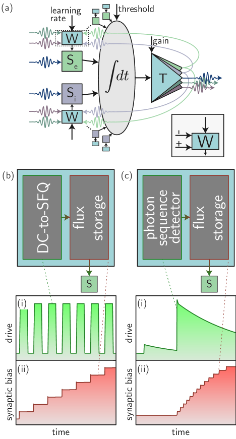
The circuits described in this work modify in either a supervised manner using JJs or unsupervised manner using SPDs in conjunction with JJs. Qualitative explanation of the memory update process in shown in Fig. 1(b) for supervised learning and in Fig. 1(c) for unsupervised learning. For the simplest binary synapse, a flux-quantum memory cell can be used to switch between the strong and weak synaptic states in 50 ps. This binary design can be extended to a multi-stable synapse that can modify the synaptic weight between the fully potentiated and fully depressed states with hundreds of stable intermediate levels, and implementations with more or less resolution are straightforward to achieve. For unsupervised learning, we consider a circuit that can implement a Hebbian learning rule that potentiates a synaptic connection using one photon from the pre-synaptic neuron and one photon from the post-synaptic neuron. We generalize this circuit to implement full spike-timing-dependent plasticity (STDP) wherein a synaptic weight can be either potentiated or depressed based on Hebbian and anti-Hebbian timing correlations. This STDP circuit uses single-photon signals at four ports. Implementations of short-term plasticity, homeostatic plasticity, and metaplasticity are discussed in the Appendices. Combining these synapse designs, it is possible to realize neurons with a distribution of synapses that update at different rates as well as ensembles of neurons wherein different neurons store information about different stimuli learned at different times, thus achieving a network with rapid adaptability and long memory retention times necessary for cognition, as discussed in Ref. Shainline et al., 2018a.
II Conceptual overview
The field of neural computing Schuman et al. (2017); Liu et al. is broad and deep. A rich body of work exists wherein neural concepts are implemented in software using conventional Boolean hardware Hopfield (1982); Ackley et al. (1985); Bishop (1994); Hinton and Salakhutdinov (2006). Such technologies are usually referred to as neural networks. We make the distinction that neural computing utilizes hardware with neural behavior present in the physics of the devices that implement the required computations rather than implementing the neural computational functions with algorithms in software. Software neural nets and neural hardware are both useful and both have promise to affect the advanced computing landscape in coming years.
We further delineate two main modes of operation of neural computers. In one mode, controlled inputs are presented to the system, and the system provides an output. The output from the system is compared to a desired output, and an error is calculated based on a cost function. This error is then used to update the configuration of the system, often through backpropagation Nielsen (2015). We refer to this mode of operation as “supervised learning”. Most technologies commonly referred to as machine learning or deep learning operate in this mode. The objective of supervised learning is often to train the hardware to perform a specific task Silver et al. (2016).
For larger neural systems performing general cognitive functions, it is advantageous to operate in an unsupervised manner. In supervised learning, there is an external means by which properties affecting network operation can be adjusted (such as by explicitly changing synaptic weights or neuron thresholds). In unsupervised learning, no such external control is available. Unsupervised learning is scalable in that the user is not required to calculate or adjust the network parameters, so systems with many more degrees of freedom can be realized. Yet unsupervised learning requires that internal activity of the network be capable of adjusting the degrees of freedom to form a useful representation of the information it is expected to process. Unsupervised learning usually occurs within spiking dynamical systems. In these dynamical systems, modification of the synaptic weights changes the structure of the network and therefore adapts the dynamical state space Sporns et al. (2000); Buzsaki and Draguhn (2004) based on external stimulus and internal network activity.
In the present work, we are interested in both supervised and unsupervised modes of operation, and we focus on the means by which synaptic weights can be modified either externally or internally to enable training and learning. In unsupervised learning, we are interested in systems that will interact continuously with their environment, be capable of immediately assimilating new information, and also capable of remembering events as long as possible. Such competing memory demands are sometimes referred to as the adaptability-precision trade-off Khorsand and Soltani (2017), and the best-performing synapses in this regard are complex Fusi et al. (2005) and may have many stable levels Fusi and Abbott (2007). In human subjects, memories have been observed to fade with a power law temporal dependence Wixted and Ebbesen (1991, 19978). It is difficult to do better than power law forgetting with plastic synapses that continually adapt Fusi et al. (2005), and simple synapses lose their memory trace most quickly Fusi and Abbott (2007). In the present work, we show synapses with a number of stable states ranging from two to hundreds. These synapses have dynamically variable memory update rates, making the synapses suitable for power law memory retention.
The neurons under consideration have been described in Ref. Shainline et al., 2018b, and they are referred to as loop neurons. They will be employed in the context of superconducting optoelectronic networks described in Refs. Shainline et al., 2017 and Shainline et al., 2018a. In such networks, light is used to communicate signals between neurons, and when a single photon is received at a synapse, the signal is converted to a number of flux quanta Tinkham (1996); Duzer and Turner (1998); Kadin (1999). We refer to this as a synaptic firing event. In such a neuron, the role of the synaptic weight is to change how many flux quanta are generated during a synaptic firing event. This determines how much current is added to the neuron’s current integration loop Shainline et al. (2018b), and therefore how close the neuron is to reaching threshold. When one or more synaptic firing events add sufficient current to the neuron’s integration loop to reach threshold, the neuron is induced to produce a pulse of light, which is distributed to that neuron’s downstream connections. Threshold detection and pulse production are treated in Ref. Shainline et al., 2018c.
The objective of this paper is to describe the means by which the synaptic weight can be modified to enable dynamically reconfigurable synapses. The photon-to-fluxon transduction that occurs during a synaptic firing event is implemented with an SPD in parallel with a JJ, as described in Ref. Shainline et al., 2018b. To change the number of fluxons generated during the synaptic firing event, one can simply change the current bias across this JJ, referred to as the synaptic firing junction. The circuits presented here are designed to dynamically modify the current bias to the synaptic firing junction, (see Fig. 2 of Ref. Shainline et al., 2018b). We refer to the circuits that modify as the synaptic update circuits. In general, there will be a chosen weakest synaptic strength and strongest synaptic strength at each synapse, and in general the weakest synaptic strength will be achieved with . Thus, it is the goal of the synaptic update circuit to vary over some range . In certain contexts it is sufficient for to only be able to take two values Liu et al. , while in other learning environments it may be advantageous to be able to achieve many values of between and . Discussion of synapses for learning in various contexts is presented in Sec. VI.
One means of modifying the current bias to the synaptic firing junction is depicted in Fig. 2. For systems with many neurons each with many synapses, we would like to use a single current source to establish the baseline synaptic bias to all synapses ( in Fig. 2), keeping in mind that we may need the baseline synaptic bias to be different for different synapses. This can be achieved by using a single current bias, , and using mutual inductors to couple this current to each synapse. The synaptic firing circuit is thus biased by a superconducting loop, referred to as the synaptic bias (SB) loop, and the objective of the synaptic update circuit is to change the current in the SB loop, also through mutual inductors. The circuits presented throughout this work achieve the various synaptic states by changing the amount of flux trapped in another superconducting loop, referred to as the synaptic storage (SS) loop. This basic concept is shown in Fig. 2, where the SB loop is coupled to both the main bias, , and the dynamic synaptic bias based on the flux trapped in the SS loop. All circuits presented in the remainder of this work provide a means to adjust the flux stored in the SS loop.
To implement supervised learning, we would like to control the flux stored in the SS loop using simple control signals, which we take to be square current pulses. In Sec. III we show that such current pulses can be used to modify the flux in the SS loop and therefore to implement binary synapses as well as multistable synapses with many hundreds of levels between and . To implement unsupervised learning, it is necessary for neuron-generated signals to be capable of modifying the flux in the SS loop. In Secs. IV and V we show how photonic signals can be used to change the state of flux in the SS loop and therefore implement learning rules based on timing correlations between the two neurons associated with each synapse.
III Supervised learning
Several quantities determine the behavior of a synapse. These include the minimum and maximum values of the synaptic weight and the number of increments between the two. For many applications in machine learning, neural networks, and neuroscience, synapses are treated as binary elements that can switch between strong (potentiated) and weak (depressed) states Amit and Fusi (1994); Fusi and Abbott (2007); Liu et al. . Memory storage times can be improved if synapses have a large number of stable states between maximally potentiated and depressed states Fusi and Abbott (2007). In Ref. Shainline et al., 2018b it was shown that, in a superconducting optoelectronic neuron, changing from 1 µA to 3 µA changes the contribution to the neuron’s integrated signal by a factor of 15. In this section, we demonstrate that the synaptic current can be changed over this range by adding anywhere from one to hundreds of fluxons to the SS loop, thereby achieving a range of synapses from a simple binary synapse to a multistable synapse with a pseudocontinuum of stable values.
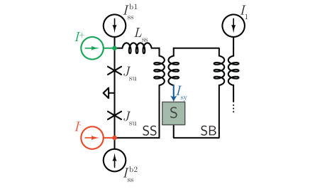
The circuit for enacting a binary synapse is shown in Fig. 2. This circuit is a standard flux-quantum memory cell Kadin (1999); Duzer and Turner (1998) coupled to the SB loop via a mutual inductor Mizugaki et al. (2005). The current delivered to the synapse, , is shifted by a static value determined by the bias and the mutual inductors shown in Fig. 2. When there are no fluxons in the SS loop, µA, the minimum value. In this state, the bias currents ( and ) are chosen such that a weakening synaptic update signal () cannot add a fluxon to the loop, so the synaptic weight cannot be further depressed. A strengthening signal can, however, switch and add one fluxon to the loop. This transitions the circuit to the potentiated state, wherein µA. At this point, further potentiating signals cannot add additional flux to the loop. The loop can store only a single fluxon, and it is characterized by Kadin (1999); Duzer and Turner (1998). The junction and circuit parameters are given in Appendix A. All parameters are typical for superconducting electronic circuits and straightforward to realize in hardware.
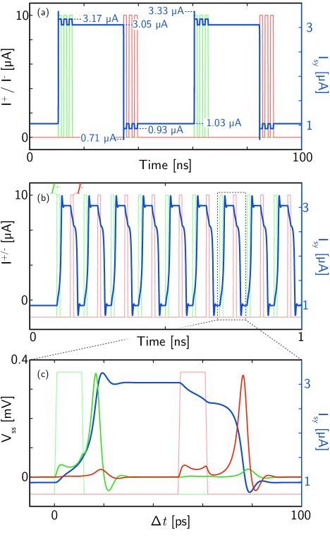
Figure 3 shows WRSpice Whiteley (1991) simulations of the temporal behavior of the circuit as it switches between states. In Fig. 3(a), the circuit is initially in the depressed state. A pulse of 10 µA drives the circuit to the potentiated state. Repeated current pulses do not switch the state, and after the input pulses cease, the cell holds the value of . Upon the application of a single 10 µA pulse into the weakening port, the circuit switches back to the depressed state, and repeated applications of this signal do not further switch the circuit.
In Fig. 3(b) we show the synapse switching between the depressed and potentiated states every 50 ps. The time scales of Fig. 3 are extremely fast compared to biological neural circuits. The speed of these circuits offers intriguing possibilities, as discussed in Sec. VI. Figure 3(c) shows a temporal zoom of a full cycle of the binary synapse occurring within 50 ps.
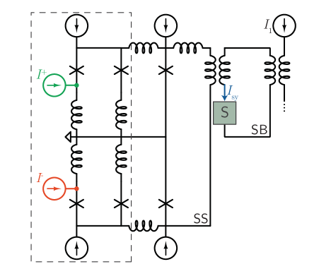
For deep learning in neural networks, it is often necessary to increment the synaptic weights in small steps. To achieve fine weight update, a superconducting loop capable of storing more than one flux quantum is utilized, as shown in Fig. 4. Flux quanta can be added one by one using DC-to-SFQ converters Kadin (1999); Duzer and Turner (1998). The binary synapse of Figs. 2 and 3 has been modified to include two DC-to-SFQ converters: one for potentiating and one for depressing. When a fluxon is produced by the potentiating DC-to-SFQ converter by the introduction of a current pulse, , the fluxon is added to the SS loop. When a fluxon is produced by the depressing DC-to-SFQ converter by the introduction of a current pulse, , the fluxon counter propagates in the SS loop. The inductors of the SS loop, and can be chosen over a broad range of values to determine the learning rate and range of synaptic weights achieved.
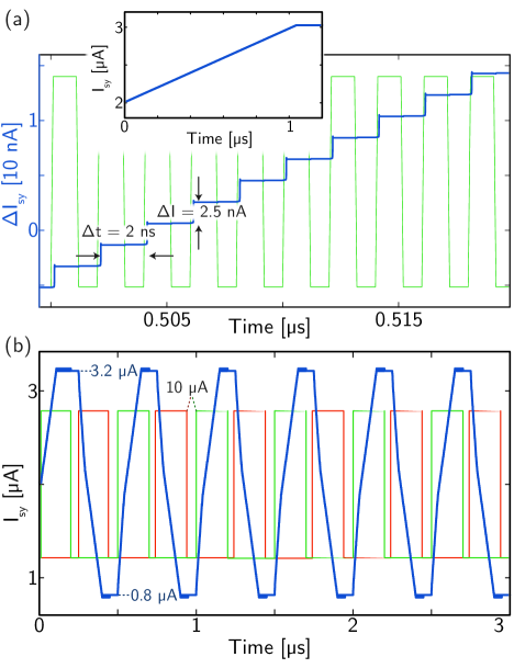
Controlled increase of synaptic bias current is again demonstrated using WRSpice Whiteley (1991). The results are shown in Fig. 5. In this calculation, a periodic square wave drives the DC-to-SFQ converter with 10 µA pulses of 1 ns duration and 2 ns period. Current is added to the SS loop in fluxon increments over many input cycles (Fig. 5(a)). In this case, the value of before any flux has been added to the SS loop is 2 µA, chosen to be in the middle of the operational range identified in Ref. Shainline et al., 2018b. For this calculation, the inductance of the SS loop is 200 nH (), leading to the addition of 2.5 nA to with the addition of each fluxon to the loop. This value of inductance (and therefore ) can be chosen over a broad range to set the synaptic update increment and number of synaptic levels. This value was chosen to create a SS loop that can store over 1000 fluxons between the minimum and maximum values of . The effects of the number of stable synaptic levels will be discussed further in Sec. VI.
The inset of Fig. 5(a) shows the behavior of as a function of time as it is potentiated to saturation. A fluxon is added to the loop every two nanoseconds. After approximately 500 fluxons have been added to the loop, the value of saturates just above 3 µA. This saturation behavior is advantageous so that a learning algorithm cannot cause a synaptic weight to grow without bound.
Figure 5(b) shows as a function of time as the potentiating and depressing DC-to-SFQ converters are alternately employed, analogous to the two drives of the binary synapse in Fig. 2. For these calculations, an SS loop with 20 nH inductance was considered to reduce the time required to achieve saturation. Initially, µA. Fluxons are added to the SS loop for 200 ns, and reaches its maximum value of 3.2 µA. Figure 5(b) shows that while the synaptic strengthening drive () is on, once the SS loop reaches saturation, the value of cannot be increased. The figure further shows that after the synaptic strengthening drive is turned off, maintains its value (i.e., during the time from 200 ns - 250 ns). After 250 ns, fluxons of the opposite sign begin to be added to the SS loop via the synaptic weakening drive (), and can be driven down to the minimum value (800 nA in this case). Cycling these drives results in the periodic behavior seen in Fig. 5(b). It can be seen that during each strengthening and weakening cycle versus time has two regions with different slopes. This is due to the fact that when the current in the SS loop is outside a certain range, the DC-to-SFQ converter releases two fluxons per drive cycle. This characteristic is likely of little consequence and may be eliminated with improved circuit design, possibly by separating the DC-to-SFQ converter from the SS loop with a JTL.
The circuits of Figs. 2 and 4 have several strengths when used to establish the synaptic weight of a superconducting optoelectronic neuron. The nature of the flux-storage Josephson circuits enables cycling and modifying the synaptic weights as many times as necessary without material degradation. The maximum and minimum values of can be designed to achieve a broad range of operating conditions. Upon reaching the maximum and minimum values, the device saturates, eliminating the possibility of runaway values of synaptic weight. Synaptic update can be carried out in a specified number of increments based on the choice of inductance of the SS loop. The size of these increments will determine the learning/forgetting rate of the synapse.
While these characteristics of the circuits are conducive to implementing a variety of training algorithms based on back propagation Nielsen (2015) or in conjunction with design through genetic evolution Floreano et al. (2008); Such et al. (2018), we would also like to enable systems that learn using only activity within the network. We next consider a Hebbian learning circuit, which strengthens the synaptic weight between two neurons that fire in succession. This will lead to the discussion of a circuit achieving STDP based on the timing correlation between pre- and post-synaptic activity.
IV Hebbian update
The Hebbian update circuit under consideration is shown in Fig. 6(a). The operation of this circuit is based on a similar principle to the supervised learning circuits discussed in Sec. III in that the synaptic bias current is adjusted based on the amount of flux stored in the SS loop. In this section we will explore how the DC-to-SFQ converter of Fig. 4 can be replaced by SPDs to enable flux to be added to the SS loop based on temporally correlated photonic activity within the network. In particular, we wish to implement a Hebbian update rule that potentiates a synaptic connection between pre- and post-synaptic neurons when the pre-synaptic neuron contributes to the firing of the post-synaptic neuron Dayan and Abbott (2001).
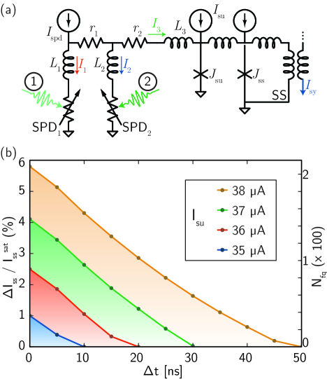
In Ref. Shainline et al., 2018b, circuits transducing photonic signals to supercurrent are discussed. The Hebbian rule requires a two-photon temporal-correlation circuit, like the temporal-code receiver of Ref. Shainline et al., 2018b, except the asymmetry of Hebbian update requires an asymmetrical initial bias to the two correlated SNSPDs. Operation of the Hebbian update circuit discussed here can be described qualitatively as follows. When no photons have been detected, the bias is directed through SPD1. The resistor ensures that SPD2 is unbiased until SPD1 receives a photon, and therefore photons incident on SPD2 have no effect on the circuit unless they are incident during a time window following a detection event by SPD1. Once a photon has been detected by SPD1, is redirected to and . The current returns to with a time constant of . If a photon is detected by SPD2 during , is predominantly redirected to , which can be sufficient to switch , the synaptic update JJ, perhaps many times depending on the bias currents, and , and the difference in arrival times between the two photons, . More details of circuit design are included in Appendix B.
During circuit operation, we assume that when the pre-synaptic neuron fires a photonic pulse, one or more photons will reach a synaptic firing circuit Shainline et al. (2018b) of the post-synaptic neuron and bring the neuron closer to its threshold Shainline et al. (2018a). We also assume additional photons have a probability of reaching SPD1 of the synaptic update circuit shown in Fig. 6(a) to perform the first step in implementing the Hebbian rule. This photon is labeled “1” in Fig. 6(a). The probability of reaching SPD1 may be controlled to modify the learning rate. Similarly, it is assumed that during a neuronal firing event, the local neuron will send photons to its downstream connections, but also to its local synapse update circuits to activate learning by striking SPD2. This photon is labeled “2” in Fig. 6(a). This self-feedback is also illustrated in Fig. 1(a).
The duration of the time window after the detection of the pre-synaptic update photon while the circuit is sensitive to the detection of the post-synaptic update photon is determined by the time constant . In Fig. 6 we analyze the current added to the SS loop as a function of the delay, , for four values of with fixed at A. We plot the change in current in the SS loop () as a percentage of the SS loop saturation current (), during Hebbian update events characterized by delay . This plot also shows the number of fluxons created during each of the events. We see that the amount of synaptic weight modification depends strongly on the temporal delay, dropping to zero after roughly . We also see that the effect depends on , providing a means by which the memory update rate can be dynamically adjusted during operation via a DC bias current. This dependence on provides a means to implement metaplasticity, as will be discussed in Sec. VI. The quantity represents the fraction of the synapse dynamic range that is acquired in a synaptic update event. Although the current in the SS loop (and therefore ) can only change by an integer number of flux quanta, the use of high-kinetic-inductance flux storage loops wherein thousands of flux quanta can be stored makes this effectively an analog circuit. For the SS loop investigated in Fig. 6(a), .
Hebbian learning rules may be based on average firing rates of pre- and post-synaptic neurons or on timing between individual spikes from these neurons Gerstner and Kistler (2002). Here we consider the latter. A timing-dependent learning rule often takes the form of exponential decay as a function of the difference in arrival times of pre- and post-synaptic signals. The form shown in Fig. 6(b) is slightly different due to Josephson nonlinearities. This modified temporal dependence is likely of little consequence as it maintains the principal function of timing-dependent plasticity, which is to modify the synaptic weight based on temporal correlation within a specified time window surrounding a neuronal firing event.
While the quantity represents the change in synaptic weight due to one Hebbian update event, the area under the curves in Fig. 6(b) will be related to the learning rate when averaged over many events, because the delay between the two photons, , will vary across events. In Fig. 6(b), the integral of the curve with µA is 3.6% of the integral of the curve with µA. For µA, the value is 18%, and for µA, the value is 48%. This indicates we can dynamically change the learning rate across a broad range by adjusting . A metaplasticity circuit accomplishing this is discussed in Appendix F.
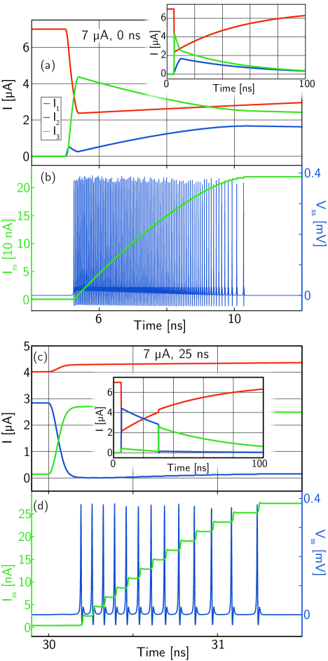
To further illustrate the performance of this device and provide intuition regarding operation, Fig. 7 shows details of the operation during Hebbian update events for cases with ns (Fig. 7(a) and (b)) and with ns (Fig. 7(c) and (d)). In these calculations, the SPDs were modeled in WRSpice as transient resistances of 5 k lasting for 200 ps introduced at a specified moment of photon detection. Figures 7(a) and (c) show the currents , , and during the time when the junction is switching. The insets of Figs. 7(a) and (c) show a 100 ns window, capturing the SPD recovery over a longer time. Figures 7(b) and (d) show the increase in the current circulating in the SS loop as well as the voltage pulses as fluxons enter the loop. We see that the Hebbian update events introduce 25 nA - 200 nA to the SS loop. With these values, 280 events with ns or 35 events with ns will saturate the SS loop. The number of events that saturate the loop can be adjusted with the SS loop inductance and with .
While it is helpful to demonstrate a Hebbian update mechanism using two photons coupled to a simple JJ circuit, learning rules that can both strengthen and weaken the synaptic connection are required for neural computing.
V Spike-timing-dependent plasticity
The STDP we seek to implement performs the Hebbian potentiating operation described in Sec. IV, but also enforces an anti-Hebbian depressing rule wherein a neuronal firing event at the post-synaptic neuron followed closely by a neuronal firing event at a pre-synaptic neuron depresses the synaptic weight between the two neurons. A circuit capable of producing this STDP is depicted in Fig. 8(a). Much as strengthening and weakening were accomplished in Sec. III by adding a mirror image of the strengthening circuit to the SS loop, here we duplicate the Hebbian circuit of Sec. IV to achieve STDP. The similarity of the SPD circuit of Fig. 8(a) and the JJ circuit of Fig. 5(a) is apparent.
The symmetry between the strengthening and weakening receiver circuits in the STDP circuit of Fig. 8(a) is broken based on whether the SPD that is biased in the steady state receives photons from the pre-synaptic or post-synaptic neuron. In the synaptic-weakening receiver circuit, a post-synaptic photon detected by SPD3 followed by a photon from a pre-synaptic neuron detected by SPD4 introduces counter-circulating flux to the SS loop. The time constants and biases of the strengthening and weakening receivers can be adjusted independently.
The WRSpice calculation shown in Fig. 8(b) and (c) illustrates the circuit in operation. Two synaptic strengthening events and two synaptic weakening events occur. The currents associated with synaptic strengthening and weakening, and are shown in Fig. 8(b). The synaptic bias current delivered to the synaptic firing junction Shainline et al. (2018b) is shown in Fig. 8(c).
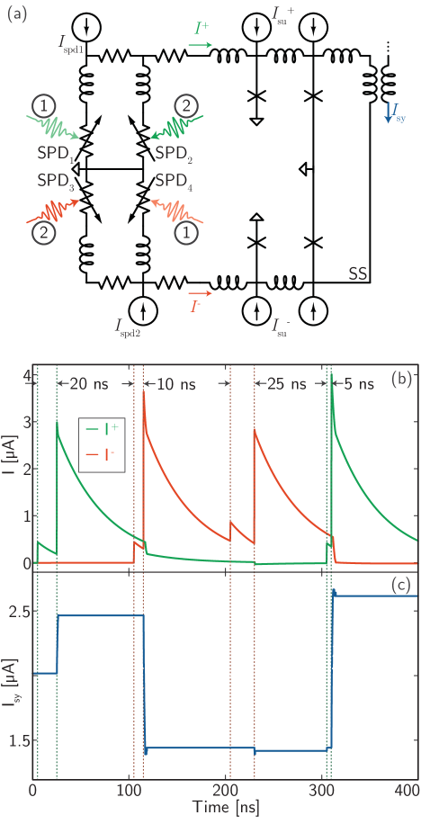
A synaptic strengthening event occurs with ns, followed by a weakening event with ns and another with ns. A final strengthening event occurs with ns. The synaptic bias current, , is observed to respond as expected based on the Hebbian analysis in Sec. IV. In this calculation, nH, and we mention again that the amount of current added to and therefore during a synaptic update event can be linearly scaled with in hardware and with dynamically. Below a certain value of photon detection will not occur, and memory update will cease. The memory update rate of the STDP synapse can be controlled by adjusting the frequency of photon absorption events. This consideration and others related to implementation of these circuits are discussed in Sec. VI.
The circuit of Fig. 8(a) induces STDP based on photon detection events from the pre- and post-synaptic neurons. It may also be possible to achieve STDP entirely in the electronic domain through the electrical signals produced during synaptic firing events and neuronal firing events. One means to use fluxon signals while setting correlation time constants with (as shown in Fig. 8) is to use fluxons to switch the gate of an nTron McCaughan and Berggren (2014). In Ref. Shainline et al., 2018c we show this operation in the context of a neuronal thresholding element. For STDP, the SPDs could be replaced with nTrons. Fluxons generated by during synaptic firing events would represent pre-synaptic activity and would switch the gates of nTrons replacing the left SPDs in Fig. 8(a). Fluxons generated by the thresholding junction, Shainline et al. (2018c), would switch the gates of nTrons replacing the right SPDs in Fig. 8(a). Hebbian and anti-Hebbian rules would be implemented based on temporal correlation between pre- and post-synaptic activity, and no photons would need to be expended for the operation. Yet the complexity of Josephson circuitry at each synapse would increase.
While crucial to learning and the interplay between the structure and function of neural systems, STDP is only one of many synaptic plasticity mechanisms. Despite their significance, discussion of short-term plasticity, homeostatic plasticity, and metaplasticity are relegated to Appendices D, E, and F. Discussion of how the parameters of the circuits presented here map to learning rate and enable quick adaption alongside long-term memory retention is presented in Appendix G.
VI Discussion
This work has explored synaptic update circuits capable of delivering a variable synaptic bias current to the synaptic firing circuits presented in Ref. Shainline et al., 2018b. We have investigated manipulation of the synaptic weight through external input of square wave pulses, as would be desirable for supervised learning, as well as manipulation of synaptic weight via photon detection events, as would be desirable for unsupervised learning. As an extension of supervised learning, it is interesting to consider using JJ circuits for fast control of synaptic weights. Using Josephson driver circuits Herr et al. (2011); Likharev (2012); Benz et al. (2015), synaptic weights could be precisely dynamically controlled. In Sec. III we showed simulations of cycling between weak and strong synaptic weights with no perceptible hysteresis at 10 GHz. Firing rates of superconducting optoelectronic neurons are likely to be limited to below 1 GHz due to SPD recovery time and emitter lifetime. Operation with network cycles having oscillation frequencies up to 20 MHz is likely. The potential to vary synaptic weight at much higher frequencies (10 GHz) introduces the possibility that synaptic connections could be weighted in the frequency domain. The same synaptic weight between two neurons could be strong in some Fourier components and weak in others.
For unsupervised learning, we considered circuits combining single–photon detectors and Josephson junctions to implement unsupervised synaptic update rules based on photons received from correlated neuronal firing events. For full spike–timing–dependent plasticity, the synaptic update circuits described here provide ports for four photons: one strengthening photon from both the pre–synaptic and post–synaptic neuron, and one weakening photon from both the pre–synaptic and post–synaptic neuron. For a single synaptic strengthening or weakening event, two of these photons must be present. When optically implementing a synaptic update rule based on timing correlation, it is difficult to achieve a circuit requiring fewer than two photons.
Other forms of photonic synapses have recently been developed and offer utility in multiple neural contexts Prucnal and Shastri (2017); Tait et al. (2014, 2017); Shen et al. (2016); Cheng et al. (2017). One can leverage phase shifts in microrings Tait et al. (2014, 2017) or Mach-Zehnder interferometers (MZIs) Shen et al. (2016) to adjust synaptic weight. Thermal tuning is often employed to implement the phase shifts. Thermal tuning requires more power than is suitable for this hardware platform. Phase shifters may be also be large if MZIs are used, and phase shifters may require exotic materials, which limit scaling if electro-optic effects are leveraged. If different synaptic channels are addressed with different frequencies of light, the out-degree of a node in the network is limited by the multiplexed channel spacing. Approaches using MZIs for weighting and routing have the disadvantage that STDP cannot be implemented because modifying a single phase shifter in the network affects many synaptic weights. One approach to synaptic weighting in the photonic domain utilizes a variable optical attenuator at each synaptic connection. Phase-change materials have been employed as such variable attenuators Cheng et al. (2017), and the absorption of phase change materials can be affected with pulses of light, thus introducing a Hebbian-type synaptic weight update process. While such an approach may be useful for certain types of neural circuits, update of these synapses requires too many photons to be useful for the energy-efficient neural computing scheme developed here (billions of photons per update operation for phase change versus single photons for superconducting optoelectronics). It is also not clear how anti-Hebbian synaptic update can be introduced to enable full spike-timing-dependent plasticity. It remains to be seen if other synaptic operations such as short-term plasticity, homeostatic plasticity, and metaplasticity can be achieved with phase-change materials. Synaptic weights that attenuate a signal in the optical domain require more light from neuronal firing events, and many photons are simply absorbed at weak synapses. By contrast, using photons for communication but weighting in the superconducting domain, as presented here, uses fluxons to change the synaptic weight, and they can be generated with orders of magnitude less energy than photons. While all of these approaches to synaptic weighting may be useful in different contexts, we have developed the synapses presented in this work based on simultaneous considerations of power, complexity, scalability, speed, and size in the context of the superconducting optoelectronic hardware platform Shainline et al. (2017, 2018a).
An important weakness of the synapses presented here is they lose all memory when superconductivity is broken. The neuromorphic system must remain below to preserve what has been learned. This class of Frosty the Snowman memory may be augmented by devices that can be heated, such as magnetic Josephson junctions Russek et al. (2016); Schneider et al. (2017, 2018). It would be appealing if the state of memory in the plastic synapses described here could be transferred to long-term magnetic memory, perhaps during a sleep phase.
Another potential challenge for this type of memory in loop neurons is flux trapping. The synaptic integration loops discussed in Ref. Shainline et al., 2018b are likely to include resistors to give a leak rate. Trapped flux in those loops will be less problematic. The synaptic storage loops that set the synaptic weights are intended to store flux for a long time to maintain memory, so they will not include resistors. In this case, trapped flux will produce variations in the initial synaptic weights across an ensemble. For binary synapses, this will result in some synapses being initialized with strong synaptic weight, and some with weak. For SS loops with high inductance, stray flux will induce a small current, so the perturbation may be small relative to the dynamic range of the synapse. For large ensembles of synapses, the statistical variation may be tolerable or even advantageous. If flux proves problematic, techniques used to shield superconducting qubits can be employed Corcoles et al. (2011).
In Ref. Shainline et al., 2018a we argue that a dynamical system capable of differentiated processing and information integration across spatial and temporal scales underlies cognition. In Ref. Shainline et al., 2018b we introduced the relaxation oscillators and dendritic processing loops capable of implementing the temporal synchronization operations necessary for integrating information in time. Network synchronization and synaptic plasticity are mutually constructive phenomena in that synaptic strengthening through spike timing is more likely to occur when the firing of two neurons is correlated, and the strengthened synapses, in turn, make the correlated neurons more likely to synchronize. Networks with small-world structure Watts and Strogatz (1998); Sporns (2010) and dynamics characterized by self-organized criticality are crucial to achieving information integration. Hebbian learning rules and STDP have also been shown to convert random networks into small-world networks and to give rise to self-organized criticality Siri et al. (2007); Rubinov et al. (2011). Creation of hardware capable of supporting complex networks and synaptic learning mechanisms will provide a powerful tool for the investigation of the relation between critical network dynamics and cognitive function. In the present work we have shown the complex synaptic behavior necessary for rapid adaptation, long-term memory retention, and synaptic update based on network activity. Networks of neurons connected by these synapses will be capable of integrating information learned at many times in many contexts in a single dynamical state.
This work has focused on changing synaptic weights in superconducting optoelectronic neurons. A central question of the hardware platform remains: how are the photons created? This question is addressed in the next paper in this series, Ref. Shainline et al., 2018c.
This is a contribution of NIST, an agency of the US government, not subject to copyright.
Appendix A Circuit parameters of supervised memory cells
The memory cell of Fig. 2 has been designed with the following circuit parameters. µA, µA, pH. The four inductors comprising the two mutual inductors are labeled from left to right. Their values are pH, pH.
The memory cell of Fig. 4 has been designed with the following circuit parameters. The inductors comprising the DC-to-SFQ converter are, from left to right, pH, pH, pH. The bias to the DC-to-SFQ converter is µA. The drive current pulses are µA with 100 ps rise and fall time and 1 ns duration. The bias to the JJ in the SS loop is µA. The mutual inductor parameters between the SS loop and the SB loop and from the SB loop to are, from left to right pH, pH, pH, pH, and µA. With nH, nA per pulse, nA per pulse. The SS loop can store µA µA.
In this work, all Josephson junctions have µA. In contrast to the circuits of Ref. Shainline et al., 2018b where JJs with µA were used, these JJs do not switch with every synaptic firing event, and consequently, using lower for power minimization is less important. Using µA leads to circuits with wider operating margins and ease of fabrication. We argue in Refs. Shainline et al., 2018c and Shainline et al., 2018d that using JJs with µA for the circuits of Ref. Shainline et al., 2018b would also be satisfactory. The JJs in this work Shainline et al. (2018b) have been simulated with , corresponding to slightly over-damped junctions Duzer and Turner (1998); Kadin (1999).
Appendix B Considerations for Hebbian circuit design
To achieve the desired Hebbian operation with the circuit of Fig. 6(a), several considerations are pertinent. When SPD1 detects a photon, it needs to direct current predominantly to , and not to . When SPD2 detects a photon, it needs to direct current predominantly to , and not to . These considerations inform us that we should choose and . We choose nH for this study. Such a small SPD may have reduced detection efficiency, but the inefficiency is tolerable for this purpose, because synaptic update will occur only rarely to optimize memory retention Fusi and Abbott (2007); Liu et al. . We then choose nH, and µH. The choices for and are made to achieve the desired temporal behavior. The time constants must be long enough to ensure the SPDs do not latch. Beyond this, they can be chosen to achieve the desired learning performance. We choose ns and ns to facilitate WRSpice analysis, but longer time constants may be necessary in practice.
The circuit parameters relevant to Fig. 6(a) are as follows. Inductor values are µH, nH, nH. µA - 10 µA. The bias to the synaptic update junction is µA, and the bias to the synaptic storage junction is the same. The resistors and can be chosen to achieve the desired correlation time window.
Appendix C Synaptic update circuit supplying synaptic firing circuit
The circuit configuration combining the synaptic update circuit of this work with the synaptic firing circuit of Ref. Shainline et al., 2018b is shown in Fig. 9. Bias current can be used to supply many synapses. A buffer stage ( and ) isolates the SI loop from flux generated during synaptic firing events.
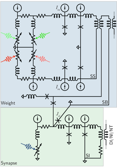
Initial simulations of this configuration show that the buffer can employ junctions with having 10 µA (same as of Ref. Shainline et al., 2018b), and with 40 µA used throughout this work.
Appendix D Short-term plasticity
Short term plasticity varies the post-synaptic response to a pre-synaptic pulse train Abbott and Regehr (2004) on a time scale close to the inter-spike interval Dayan and Abbott (2001). Short term plasticity acts as a filter, and the response can be low-pass, high-pass, or band-pass depending on a number of factors. These various filtering operations can be achieved in loop neurons with the addition of typical SPD/JJ loop circuits that change their state in response to pre-synaptic activity, either from photons from the pre-synaptic neuron or fluxons generated during the synaptic firing event. A circuit that may be utilized to perform the filtering operations of short-term plasticity using additional JJs and the fluxons produced during a synaptic firing event is shown in Fig. 10. This circuit expands upon the synaptic receiver circuit of Ref. Shainline et al., 2018b. Two additional JJs have been added in series to the junction in the Josephson transmission line, . These JJs are coupled to independent loops that are inductively coupled to the synaptic bias loop. In the absence of synaptic activity, the bias is set by , just as before. However, during a synaptic firing event, the two additional junctions also switch. Therefore, flux is coupled to the synaptic integrating loop, as before, but flux is also added to two new loops, the short-term facilitating loop (SF), and the short-term depressing loop (SD). The SF loop will add current to , effectively strengthening the synaptic weight, and the SD loop will reduce the current to , effectively weakening the synaptic weight. Therefore, the sign of the mutual inductance of the two loops is opposite, and their magnitude may differ. The time constants of the SF and SD loops can be set independently, and they will likely be slightly longer than the inter-spike interval of pulse trains in the system ( 1 µs). A given synapse may employ one or both loops as required for information processing, and a given neuron is likely to benefit from an ensemble of synapses with diverse short-term filtering responses.
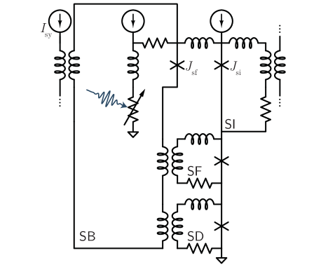
Short-term facilitation may operate such that the first pre-synaptic pulse evokes no post-synaptic response, and only after several pulses has the synaptic weight been facilitated to the point of communicating subsequent pulses. The circuit of Fig. 10 would need to be modified to achieve this behavior, as facilitation and depression both depend on the switching of the junctions, which requires successful pre-synaptic transmission. Such short-term facilitating behavior can be accomplished by introducing an additional SPD explicitly for short-term plasticity. This SPD would receive photons from the pre-synaptic neuron, just as the SPD in the receiver circuit shown in Fig. 10, but the additional SPD would add no flux to the SI loop upon firing, and would instead only adjust the flux in the SF and SD loops.
Appendix E Homeostatic plasticity
The function of homeostatic plasticity is to modulate synaptic efficacy in response to a running average of post-synaptic neuronal activity to keep neuronal gain within a useful dynamic range Cooper and Bear (2012a). A loop neuron circuit can implement homeostatic plasticity with fluxons generated by thresholding events of the post-synaptic neuron. One means to achieve this operation is shown in Fig. 11.
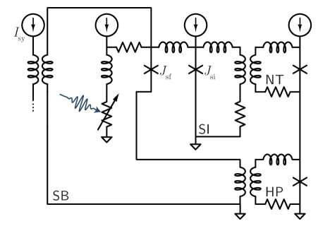
Whereas the short-term plasticity circuit of Appendix D made use only of signals generated by a synaptic firing event, the homeostatic plasticity circuit makes use only of signals generated by post-synaptic neuronal firing events. The homeostatic plasticity (HP) loop is negatively inductively coupled to the synaptic firing junction (), meaning flux added to HP reduces the bias to , thereby depressing the synaptic efficacy. By choosing an time constant for the HP loop that is longer than the neuron’s typical inter-spike interval, the negative HP feedback depends on a sliding temporal average of post-synaptic neuronal firing activity Bienenstock et al. (1982).
Appendix F Metaplasticity
Homeostatic plasticity (Appendix E) is one example of a plasticity mechanism that compensates for neural activity on longer time scales to adjust learning rate. Homeostatic plasticity is a response to a sliding temporal average of the post-synaptic neuron Bienenstock et al. (1982); Cooper and Bear (2012b). Metaplasticity refers more generally to mechanisms that adjust not the synaptic efficacy, but the rate of change (or probability of change) of synaptic efficacy. Here we discuss a loop circuit that achieves a metaplastic response Fusi et al. (2005); Abraham (2008); Khorsand and Soltani (2017) based on both pre-synaptic and post-synaptic activity using similar SPD/JJ circuits to those developed for the STDP circuit of Sec. V.
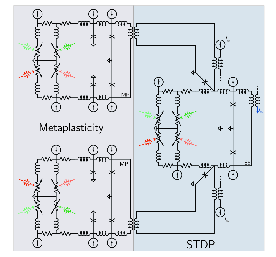
The circuit under consideration is shown in Fig. 12. The concept here is similar to many other operations in loop neurons. The fractional change in synaptic efficacy (, see Sec. VI) incurred during an STDP update event in the STDP circuit of Sec. V depends on the magnitude of the current through the junctions in parallel with the SPDs. The function of the metaplastic circuit of Fig. 12 is to modify these bias currents based on correlated pre-synaptic and post-synaptic activity. To achieve this operation, the same circuit block that is employed to adjust during a plasticity (efficacy update) event is also employed to adjust the JJ bias during a metaplasticity (learning rate update) event. With this circuit, the amount the synaptic efficacy is adjusted during an STDP update event depends on the flux trapped in the metaplasticity (MP) loops. The learning rate depends on both the efficacy update frequency as well as the magnitude of each update (see Sec. VI). Thus, by changing the magnitude of the updates, the metaplastic circuits modify the learning rate.
Considering the metaplastic circuits in the context of the synapse as a whole Shainline et al. (2018b), the state of the synapse is associated with the flux in the synaptic integrating loop. The rate of change of the state of the synapse is associated with the flux in the synaptic storage loop. The rate of change of the rate of change of the state of the synapse is associated with the flux in the metaplasticity loops. By cascading additional loops, one can continue the hierarchy of synaptic loops that record the state of the synapse and its derivatives. We suspect the three levels of hierarchy presented here will suffice for many applications.
At this point, a basic algorithm for loop neuron design has emerged. For each synaptic function, add an SPD, a JJ, and a loop. Inductively couple the loop bias currents as functionally appropriate. Choose time constants carefully. Repeat until there is no more space. As the number of plasticity operations, and therefore SPDs, JJs, and loops, grows large, it may be possible to reduce the component count by using the same SPDs, JJs, and loops for multiple operations.
The circuits for various forms of synaptic plasticity presented in these Appendices are motivated qualitatively, and superior designs are undoubtedly possible. The circuit implementations for STDP, short-term plasticity, homeostatic plasticity, and metaplasticity are intended to convey the potential for diverse synaptic functionality achievable with superconducting optoelectronic circuits in the context of loop neurons. Because synaptic operations use few photons and fluxons, they are energy efficient. Scaling in complexity will likely be limited by fabrication challenges and device real estate.
Appendix G Learning rate and memory retention
To discuss synaptic update, it is helpful to define several parameters. We follow the conventions of Refs. Fusi et al. (2005) and Fusi and Abbott (2007). We refer to the normalized synaptic weight as , where corresponds to the minimum synaptic weight (in general not corresponding to a synaptic efficacy of zero), and corresponds to the maximum synaptic weight. The spacing between synaptic levels is denoted by . The total number of stable synaptic states between and is . Reference Fusi et al., 2005 defines a candidate plasticity event as “the occurrence of a pattern of activity that could potentially lead to synaptic modification.” These event occur at a rate . The probability that one of these events is a candidate for strengthening (Hebbian) is , and the probability that it is a candidate for weakening (anti-Hebbian) is . The symbol denotes the “size of the potentiation and depression modifications” when synaptic update occurs Fusi and Abbott (2007). Synaptic strengthening occurs at a rate , and weakening occurs at a rate . The synaptic efficacy update rates as a fraction of the full synaptic efficacy range are given by and . The initial signal–to–noise ratio of a memory upon storage is denoted by , and is proportional to the number of synapses which have been modified by the memory.
In the context of the circuits described here, is related to the synaptic bias current, , which determines the synaptic efficacy. The synaptic efficacy is manifest physically as the current added to the NI loop during a synaptic firing event Shainline et al. (2018b). In this work we have been treating A as the state of the synapse, and A as the state of the synapse. For the binary synapse of Figs. 2 and 3, . For the multi–stable synapse of Figs. 4 and 5, was shown to be nearly 1000. is determined by the synaptic storage loop inductance, and can take a wide range of values. The rate at which candidate Hebbian and anti-Hebbian events occur depends on the firing rates of the network, and this parameter is normalized out of analyses of memory retention times. The probabilities and also depend on network activity and in general cannot be relied upon to be precisely balanced Fusi and Abbott (2007). In the circuits described here, and can be engineered by changing the number of photons that are directed to the STDP receiver SPDs during each neuronal firing event. This number of photons can be much less than one so that a single photon is rarely directed for plasticity and synaptic update is infrequent. For example, we may operate in a mode wherein a pre–synaptic neuron sends one photon to each downstream synaptic firing port, one photon to each downstream synaptic update strengthening port, and one photon to each downstream synaptic update weakening port during each neuronal firing event. The rate at which the post–synaptic neuron sends photons to its own synaptic update ports then controls and . This hardware-defined means of setting and can vary across a synaptic population. This approach to slow stochastic learning has the benefit of requiring few photons per neuronal firing event. A neuronal firing event would need to produce photons, where is the number of synaptic connections directed away from the firing neuron.
The size of synaptic modifications, , is determined in the STDP circuit by the values of , , , and . As shown in Fig. 6, changing changes the amount of current added to the SS loop during a synaptic update event, and therefore changes the current bias, , which sets the synaptic weight during a synaptic firing event.
Investigation of the limits of memory retention in the presence of ongoing plasticity Fusi and Abbott (2007) reveals that memory lifetimes can be improved linearly with the number of stable synaptic states, . The expense is a decreased signal–to–noise ratio of stored memories, . Reference Fusi and Abbott, 2007 further discovered that synapses in which is a function of (“soft bounds”) performed well for extending memory storage times while maintaining high . The circuits discussed in the present work can implement such soft bounds by inductively coupling to so that approaches some minimum value as the synaptic storage loop approaches saturation.
In addition to plasticity and multi–stable synapses, power law memory retention is likely to make use of internal synaptic states Fusi et al. (2005) that do not alter the efficacy of the synapse, but do affect the probability that a future Hebbian event will update the synaptic weight as well as affect the magnitude of that update, should it occur. This corresponds to states of the synapse with different values of , but the same value of . Circuit modifications that adapt learning rate in response to internal and external activity are referred to as metaplastic Abraham (2008). Using synapses with complex internal states allows for rapid incorporation of new information while maintaining stable, long–term memories Amit and Fusi (1994); Fusi et al. (2005); Fusi and Abbott (2007); Abraham (2008); Khorsand and Soltani (2017). A route to achieve metaplasticity in the circuits presented here is to vary , the current that determines the amount of synaptic shift during an update event. Thus, in the circuits presented here, we have . By changing in time, plasticity can be present in an ensemble during a certain period of training, and then subsequently turned off, allowing those memories not to be corrupted by subsequent activity. can by dynamically varied externally to implement supervised metaplasticity, or can be modified by activity within the network using similar receiver circuits to those presented for STDP (see Appendix F). Activity dependent modification not only of , but also and (see Fig. 8) is likely to provide mechanisms to adjust synaptic update rates to ensure the dynamic range of the synapses is matched to cortical activity Bienenstock et al. (1982); Cooper and Bear (2012a) (see Appendix E).
Reference Fusi et al., 2005 elucidates that a network of heterogeneous synapses with a varying number of stable states does not outperform a network of binary synapses with multiple internal states, but a network of heterogeneous synapses with different numbers of stable states as well as multiple states was not investigated. This combination is likely to achieve the best of both worlds. The optoelectronic synapses of the present work have the opportunity to achieve spike–timing–dependent plasticity with a large number of stable levels as well as a large number of states affecting adaptation rate. If the goal is to achieve a learning system that can rapidly incorporate new information while retaining memories for a long time, neural systems must incorporate synapses that vary by different amounts and over different time scales. On a given neuron, or across an ensemble of neurons, a set of synapses may be heterogeneous in multiple capacities. The synapses may have a distribution in terms of number of stable states (), and they may have a distribution in learning rate, manifest in . Synapses that are updated infrequently and in small increments will store old wisdom. Binary synapses that switch readily bring fresh eyes. Neurons comprising primarily fresh eyes synapses bring fresh eyes to a network, and neurons comprising primarily synapses that were trained long ago and rarely change bring old wisdom. The ability to integrate information from a network of synapses with different learning rates trained at different times is advantageous for networks with optimal, power law forgetting rates. An ensemble of synapses is also likely to benefit from a diversity of short-term and homeostatic plasticity mechanisms, as discussed in Appendices D and E.
References
- Dayan and Abbott (2001) P. Dayan and L.F. Abbott, Theoretical Neuroscience (The MIT Press, 2001).
- Gerstner and Kistler (2002) W. Gerstner and W. Kistler, Spiking neuron models, 1st ed. (Cambridge University Press, Cambridge, 2002).
- Abbott and Regehr (2004) L.F. Abbott and W.G. Regehr, “Synaptic computation,” Nature Reviews 431, 796 (2004).
- Buzsaki (2006) G. Buzsaki, Rhythms of the brain (Oxford University Press, 2006).
- Siri et al. (2007) B. Siri, M. Quoy, B. Delord, B. Cessac, and H. Berry, “Effects of hebbian learning on the dynamics and structure of random networks with inhibitory and excitatory neurons,” Journal of Physiology Paris 101, 136 (2007).
- Hawkins and Ahmad (2016) J. Hawkins and S. Ahmad, “Why neurons have thousands of synapses, a theory of sequence memory in neocortex,” Frontiers in Neural Circuits 10, 23 (2016).
- Nielsen (2015) M.A. Nielsen, Neural networks and deep learning (Determination Press, 2015).
- Shainline et al. (2017) J.M. Shainline, S.M. Buckley, R.P. Mirin, and S.W. Nam, “Superconducting optoelectronic circuits for neuromorphic computing,” Phys. Rev. App. 7, 034013 (2017).
- Shainline et al. (2018a) J.M. Shainline, S.M. Buckley, A.N. McCaughan, J. Chiles, R.P. Mirin, and S.W. Nam, “Superconducting optoelectronic neurons I: General principles,” arXiv , 1805.01929 (2018a).
- Shainline et al. (2018b) J.M. Shainline, S.M. Buckley, A.N. McCaughan, M. Castellanos-Beltran, C.A. Donnelly, M.L. Schneider, R.P. Mirin, and S.W. Nam, “Superconducting optoelectronic neurons II: Receiver circuits,” arXiv , 1805.02599 (2018b).
- Gol’tsman et al. (2001) G.N. Gol’tsman, O. Okunev, G. Chulova, A. Lipatov, A. Semenov, K. Smirnov, B. Voronov, A. Dzardanov, C. Williams, and R. Sobolewski, “Picosecond superconducting single-photon optical detector,” Appl. Phys. Lett. 79, 705 (2001).
- Natarajan et al. (2012) C.M. Natarajan, M.G. Tanner, and R.H. Hadfield, “Superconducting nanowire single-photon detectors: physics and applications,” Supercond. Sci. Tech. 25, 063001 (2012).
- Liu et al. (2013) D.K. Liu, L.X. You, S.J. Chen, X.Y. Yang, Z. Wang, Y.L. Wang, X.M. Xie, and M.H. Jiang, “Electrical characheristics of superconducting nanowire single photon detector,” IEEE Trans. Appl. Supercond. 23, 2200804 (2013).
- Marsili et al. (2013) F. Marsili, V.B. Verma, J.A. Stern, S. Harrington, A.E. Lita, T. Gerrits, I. Vayshnker, B. Baek, M.D. Shaw, R.P. Mirin, and S.W. Nam, “Detecting single infrared photons with 93% system efficiency,” Nat. Photon. 7, 210 (2013).
- Verma et al. (2015) V.B. Verma, B. Korzh, F. Bussieres, R.D. Horansky, S.D. Dyer, A.E. Lita, I. Vayshenker, F. Marsili, M.D. Shaw, H. Zbinden, R.P. Mirin, and S.W. Nam, “High-efficiency superconducting nanowire single-photon detectors fabricated from mosi thin-films,” Opt. Express 23, 33792 (2015).
- Tinkham (1996) M. Tinkham, Introduction to Superconductivity, 2nd ed. (Dover, 1996).
- Duzer and Turner (1998) T. Van Duzer and C.W. Turner, Principles of superconductive devices and circuits, 2nd ed. (Prentice Hall, USA, 1998).
- Kadin (1999) Alan M. Kadin, Introduction to superconducting circuits, 1st ed. (John Wiley and Sons, USA, 1999).
- Schuman et al. (2017) C.D. Schuman, T.E. Potok, R.M. Patton, J.D. Birdwell, M.E. Dean, G.S. Rose, and J.S. Plank, “A survey of neuromorphic computing and neural networks in hardware,” arXiv , arXiv:1705.06963v1 (2017).
- (20) S.-C. Liu, T. Delbruck, G. Indiveri, A. Whatley, and R. Douglas, eds., Event-based neuromorphic systems (John Wiley and Sons).
- Hopfield (1982) J.J. Hopfield, “Neural networks and physical systems with emergent computational abilities,” PNAS 79, 2554 (1982).
- Ackley et al. (1985) D.H. Ackley, G.E. Hinton, and T.J. Sejnowski, “A learning algorithm for boltzmann machines,” Cognitive Science 9, 147 (1985).
- Bishop (1994) C.M. Bishop, “Neural networks and their applications,” Rev. Sci. Inst. 65, 1803 (1994).
- Hinton and Salakhutdinov (2006) G.E. Hinton and R.R. Salakhutdinov, “Reducing the dimensionality of data with neural networks,” Science 313, 504 (2006).
- Silver et al. (2016) D. Silver, A. Huang, C.J. Maddison, A. Guez, L. Sifre, G. van den Driessche, J. Schrittwieser, I. Antonoglou, V. Panneershelvam, M. Lanctot, S. Dieleman, D. Grewe, J. Nham, N. Kalchbrenner, I. Sutskever, T. Lillicrap, M. Leach, K. Kavukcuoglu, T. Graepel, and D. Hassabis, “Mastering the game of go with deep neural networks and tree search,” Nature 529, 484 (2016).
- Sporns et al. (2000) O. Sporns, G. Tononi, and G.M. Edelman, “Connectivity and complexity: the relationship between enuroanatomy and brain dynamics,” Neural networks 13, 909 (2000).
- Buzsaki and Draguhn (2004) G. Buzsaki and A. Draguhn, “Neuronal oscillations in cortical networks,” Science 304, 1926 (2004).
- Khorsand and Soltani (2017) P. Khorsand and A. Soltani, “Optimal structure of metaplasticity for adaptive learning,” PLOS Computational Biology (2017).
- Fusi et al. (2005) S. Fusi, P.J. Drew, and L.F. Abbott, “Casdcade models of synaptically stored memories,” Neuron 45, 599 (2005).
- Fusi and Abbott (2007) S. Fusi and L.F. Abbott, “Limits on the memory storage capacity of bounded synapses,” Nature Neuroscience 10, 485 (2007).
- Wixted and Ebbesen (1991) J.T. Wixted and E. Ebbesen, “On the form of forgetting,” Psychol. Sci. 2, 409 (1991).
- Wixted and Ebbesen (19978) J.T. Wixted and E. Ebbesen, “Genuine power curves in forgetting,” Mem. Cognit. 25, 731 (19978).
- Shainline et al. (2018c) J.M. Shainline, A.N. McCaughan, A. Jafari-Salim, S.M. Buckley, R.P. Mirin, and S.W. Nam, “Superconducting optoelectronic neurons IV: Transmitter circuits,” arXiv , 1805.01941 (2018c).
- Amit and Fusi (1994) D.J. Amit and S. Fusi, “Learning in neural networks with material synapses,” Neural Computation 6, 957 (1994).
- Mizugaki et al. (2005) Y. Mizugaki, H. Hakii, M. Moriya, K. Usami, and T. Kobayashi, “Mutual inductance coupled through superconducting thin film in niobium josephson integrated circuits,” Japanese Journal of Applied Physics 44, 1 (2005).
- Whiteley (1991) S.R. Whiteley, “Josephson junctions in spice3,” IEEE Tras. Mag. 27, 2902 (1991).
- Floreano et al. (2008) D. Floreano, P. Durr, and C. Mattiussi, “Neuroevolution: from architectures to learning,” Evol. Intel. 1, 47 (2008).
- Such et al. (2018) F.P. Such, V. Madhavan, E. Conti, J. Lehman, K.O. Stanley, and J. Clune, “Deep neuroevolution: genetic algorithms are a competitive alternative for training deep neural networks for reinforcement learning,” arXiv , 1712.06567 (2018).
- McCaughan and Berggren (2014) A.N. McCaughan and K.K. Berggren, “A superconducting-nanowire three-terminal electrothermal device,” Nano letters 14, 5748 (2014).
- Herr et al. (2011) Q.P. Herr, A.Y. Herr, O.T. Oberg, and A.G. Ioannidis, “Ultra-low-power superconductor logic,” J. Appl. Phys. 109, 103903 (2011).
- Likharev (2012) K.K. Likharev, “Superconductor digital electronics,” Physica C 482, 6 (2012).
- Benz et al. (2015) S.P. Benz, S.B. Waltman, A.E. Fox, P.D. Dresselhaus, A. Rufenacht, J.M. Underwood, L.A. Howe, R.E Schwall, and C.J. Burroughs Jr., “One-volt josephson arbitrary waveform synthesizer,” IEEE Trans. Appl. Supercond. 25, 1300108 (2015).
- Prucnal and Shastri (2017) P.R. Prucnal and B.J. Shastri, Neuromorphic photonics, 1st ed. (CRC Press, New York, 2017).
- Tait et al. (2014) A.N. Tait, M.A. Nahmias, B.J. Shastri, and P.R. Prucnal, “Broadcast and weight: an integrated network for scalable photonic spike processing,” J. Lightwave Technol. 32, 3427 (2014).
- Tait et al. (2017) A.N. Tait, T. Ferreira de Lima, E. Zhou, A.X. Wu, M.A. Nahmias, B.J. Shastri, and P.R. Prucnal, “Neuromorphic photonic networks using silicon photonic weight banks,” Nature Sci. Rep. 7, 7430 (2017).
- Shen et al. (2016) Y. Shen, N.C. Harris, S. Skirlo, M. Prabhu, T. Baehr-Jones, M. Hochberg, X. Sun, S. Zhao, H. Larochelle, D. Englund, and M. Soljacic, “Deep learning with coherent nanophotonic circuits,” Nature Photonics 11, 441 (2016).
- Cheng et al. (2017) Z. Cheng, C. Rios, W.H.P. Pernice, C.D. Wright, and H. Bhaskaran, “On-chip photonic synapse,” Science Advances 3, 1700160 (2017).
- Russek et al. (2016) S.E. Russek, C. Donnelly, M. Schneider, B. Baek, M. Pufall, W.H. Rippard, P.F. Hopkins, P.D. Dresselhaus, and S.P. Benz, “Stochastic Single Flux Quantum Neuromorphic Computing using Magnetically Tunable Josephson Junctions,” in IEEE International Conference on Rebooting Computing (IEEE, 2016).
- Schneider et al. (2017) M.L. Schneider, C.A. Donnelly, S.E. Russek, B. Baek, M.R. Pufall, P.F. Hopkins, and W.H. Rippard, “Energy-efficient single-flux-quantum based neuromorphic computing,” in IEEE International Conference on Rebooting Computing (IEEE, 2017).
- Schneider et al. (2018) M.L. Schneider, C.A. Donnelly, S.E. Russek, B. Baek, M.R. Pufall, P.F. Hopkins, P. Dresselhaus, S.P. Benz, and W.H. Rippard, “Ultralow power artificial synapses using nanotextured magnetic josephson junctions,” Science Advances 4, 1701329 (2018).
- Corcoles et al. (2011) A.D. Corcoles, J.M. Chow, J.M. Gambetta, C. Rigetti, J.R. Rozen, G.A. Keefe, M.B. Rothwell, and M. Steffen, “Protecting superconducting qubits from radiation,” App. Phys. Lett. 99, 181906 (2011).
- Watts and Strogatz (1998) D.J. Watts and S.H. Strogatz, “Collective dynamics of small-world networks,” Nature 393, 440 (1998).
- Sporns (2010) O. Sporns, Networks of the Brain, 1st ed. (The MIT Press, Cambridge, Massachusetts, 2010).
- Rubinov et al. (2011) M. Rubinov, O. Sporns, J.-P. Thivierge, and M. Breakspear, “Neurobiologically realistic determinants of self-organized criticality in networks of spiking neurons,” PLoS Computational Biology 7, 1 (2011).
- Shainline et al. (2018d) J.M. Shainline, J. Chiles, S.M. Buckley, A.N. McCaughan, R.P. Mirin, and S.W. Nam, “Superconducting optoelectronic neurons V: Networks and scaling,” arXiv , 1805.01942 (2018d).
- Cooper and Bear (2012a) L.N. Cooper and M.F. Bear, “The bcm theory of synapse modification at 30: interaction of theory with experiment,” Nature Reviews Neuroscience 13, 798 (2012a).
- Bienenstock et al. (1982) E.L. Bienenstock, L.N. Cooper, and P.W. Munro, “Theory for the development of neuron selectivity: orientation specificity and binocular interaction in visual cortex,” The Journal of Neuroscience 2, 32 (1982).
- Cooper and Bear (2012b) L.N. Cooper and M.F. Bear, “The bcm theory of synapse modification at 30: interaction of theory with experiment,” Nature Reviews Neuroscience 13, 798 (2012b).
- Abraham (2008) W.C. Abraham, “Metaplasticity: tuning synapses and networks for plasticity,” Nature Neuroscience 9, 387 (2008).