Spin wave effects in transport between a ferromagnet and a Weyl semimetal surface
Abstract
We experimentally investigate spin-polarized transport between a ferromagnetic Ni electrode and a surface of Weyl semimetal, realized in a thick WTe2 single crystal. For highly-transparent Ni-WTe2 planar junctions, we observe non-Ohmic behavior with an overall increase of differential resistance with current bias, which is accomplished by current-induced switchings. This behavior is inconsistent with trivial interface scattering, but it is well known for spin-polarized transport with magnon emission. Thus, we interpret the experimental results in terms of spin wave excitation in spin textures in the WTe2 topological surface states, which is supported by the obtained magnetic field and temperature dependencies.
pacs:
73.40.Qv 71.30.+hA strong area of interest in condensed matter physics is topological materials hasan ; zhang ; das ; chiu , which combines many non-trivial effects, table top test ground for high-energy physics theories and huge potential for applications, for example in spintronics or quantum computing. Recently new classes of topological materials with gapless bulk spectra called Dirac and Weyl semimetals have been proposed armitage . Similarly to topological insulators, Weyl semimetals have topologically protected Fermi arc surface states, which are connecting projections of Weyl nodes on the surface Brillouin zone armitage .
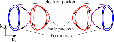
WTe2 is one of the realizations of type-II Weyl semimetal li2017 , where energy spectrum is tilted in momentum-energy space soluyanov . WTe2 demonstrates giant nonsaturating magnetoresistance ali2014 ; lvEPL15 . Now it is connected with complex spin textures in WTe2 jiang15 ; rhodes15 ; wang16 . Spin- and angle- resolved photoemission spectroscopy (SARPES) data indeed demonstrate spin-polarized surface Fermi arcs, and spin polarized Fermi pockets in bulk spectrum das16 ; feng2016 , see Fig. 1.
Intriguing spin properties of Weyl semimetals make it attractive material for spin investigations. Giant intrinsic Spin Hall Effect was recently predicted in TaAs based Weyl semimetals sun while SARPES measurements demonstrated nearly full spin polarization of Fermi arcs in TaAs lv2015 ; xu16 . Currently there are two main spin transport approaches: illumination with polarized light and spin injection from ferromagnetic contact tserkovnyak . In the latter case one can additionally expect back action of the semimetal on the ferromagnet in the form of spin-torque, which could lead even to remagnetization of ferromagnetic contact slonczewski . The generation of both out-of-plane and in-plane spin-torque has been demonstrated recently in few layers WTe2 at room temperature with ST-FMR and second harmonic Hall measurements macneill2016 . On the other hand, current-induced excitation of spin waves, or magnons, is possible at large electrical current densities for normal-ferromagnet junctions tsoi1 ; tsoi2 ; balkashin ; balashov . Thus, it is reasonable to study spin-polarized transport between a ferromagnet and a Weyl semimetal surface.
Here, we experimentally investigate spin-polarized transport between a ferromagnetic Ni electrode and a surface of Weyl semimetal, realized in a thick WTe2 single crystal. For highly-transparent Ni-WTe2 planar junctions, we observe non-Ohmic behavior with an overall increase of differential resistance with current bias, which is accomplished by current-induced switchings. This behavior is inconsistent with trivial interface scattering, but it is well known for spin-polarized transport with magnon emission. Thus, we interpret the experimental results in terms of spin wave excitation in spin textures in the WTe2 topological surface states, which is supported by the obtained magnetic field and temperature dependencies.
WTe2 compound was synthesized from elements by reaction of metal with tellurium vapor in the sealed silica ampule. The WTe2 crystals were grown by the two-stage iodine transport growth1 , that previously was successfully applied growth1 ; growth2 for growth of other metal chalcogenides like NbS2 and CrNb3S6. The WTe2 composition is verified by energy-dispersive X-ray spectroscopy. The X-ray diffraction (Oxford diffraction Gemini-A, MoK) confirms orthorhombic single crystal WTe2 with lattice parameters Å, Å, and Å.
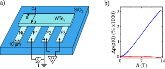
A sample sketch is presented in Fig. 2 (a). 50 nm thick nickel film is thermally evaporated on the insulating SiO2 substrate mounted on the in-plane magnetized sample holder. 10 m wide ferromagnetic leads are formed by photolithography and lift-off technique. The WTe2 crystal (with dimensions ) is transferred on top of the leads with overlap and weakly pressed to form planar Ni-WTe2 junctions.
We investigate transport properties of single Ni-WTe2 junction by a three-point technique, see Fig. 2 (a): a studied contact F2 is grounded, two other contacts F1 and F3 are employed to apply current and measure voltage respectively. To obtain characteristics we sweep dc-current modulated by low (below 2 , kHz) ac current. We measure dc and ac voltage simultaneously using voltmeter and lock-in amplifier correspondingly. Measured ac signal is independent of frequency in 1-5 kHz range, which is defined by applied ac filters.
In a three-point technique, the measured potential reflects in-series connected resistances of the Ni-WTe2 junction, some part of the WTe2 crystal, and the Ni lead with the grounding wire. To exclude the latter term, additional connection to the grounded F2 lead is used, as depicted in Fig. 2. From independence on the particular choice of current and voltage probes to the WTe2 crystal, we verify that the Ni-WTe2 junction resistance dominates in the obtained curves.
We check by standard magnetoresistance measurements that our WTe2 samples demonstrate large, non-saturating positive magnetoresistance in normal magnetic field, which goes to zero in parallel one, see Fig. 2 (b), as it has been shown for WTe2 Weyl semimetal ali2014 . To extract features specific to WTe2 Weyl semimetal surface states, the measurements are performed in a dilution refrigerator at temperatures from 30 mK to 1.2 K with different orientations of the magnetic field to the junction plane.
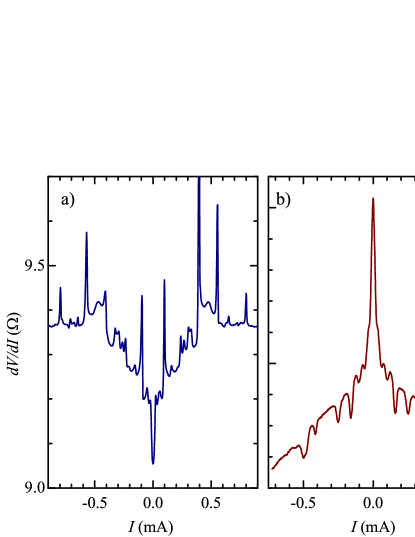
Despite of equally prepared Ni-WTe2 junctions, there are serious device-to-device fluctuations of the junction resistance. Fig. 3 provides typical examples of low-temperature characteristics for the two limiting cases.
For the transparent interface with low Ni-WTe2 junction resistance, is rising at low biases with saturation at higher ones, see Fig. 3 (a). This behavior is inconsistent with trivial impurity or roughness scattering at the interface, which can generally be described as tunneling through a potential barrier. On the other hand, an overall symmetric increase in is a familiar effect for electron scattering by emission of phonons and magnons myers .
In contrast, demonstrates clear tunnel behavior for low-transparency junctions, see Fig. 3 (b): is slightly asymmetric, the differential resistance is diminishing with bias.
For both realizations of Ni-WTe2 junctions, we observe current-induced switchings of at high currents. They appear as sharp peaks or dips in Fig. 3 (a) and (b), respectively. These features are well reproducible in different cooling cycles. They are symmetric with respect to the current sign. There is no noticeable hysteresis with the current sweep direction for experimental curves.
The observed non-linearity as well as current-induced switchings are sensitive to the magnetic field and temperature.
Fig. 4 shows temperature evolution of characteristics for high- and low-transparency junctions, see (a) and (b) panels, respectively. The effect of temperature is weak below 0.5 K. At higher temperatures, non-linearity is diminishing. Above 1 K, the differential resistance is almost constant in Fig. 4 (a), so s are of standard Ohmic behavior. In contrast, is still non-linear for the resistive junction in Fig. 4 (b), while dips are also suppressed above 1 K.
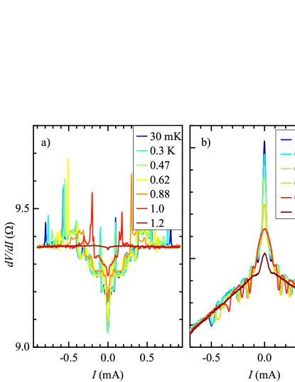
Fig. 5 demonstrates evolution of curves with magnetic field, which is applied along a, b and c WTe2 crystal axes, respectively. The effect of magnetic field is sophisticated: in high fields, the zero-bias nonlinearity is suppressed, while the level of high-current saturation is unchanged, so that curve is of clear Ohmic behavior above some magnetic field. This field is smaller for normal field orientation, see Fig. 5 (c), while there is no difference for two in-plane orientations, cp. Fig. 5 (a) and (b). In lower fields, the positions of current-induced switchings are shifting to smaller currents. The effect of magnetic field on the low-transparent junction is similar to the presented in Fig. 5. The gradual evolution of switchings’ positions also proves excellent reproducibility of these features in addition to their stability in thermal cycling.
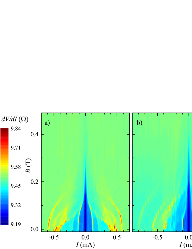
We should connect the obtained results with spin-dependent transport between a ferromagnetic Ni lead and WTe2 surface states:
(i) A ferromagnetic lead is essential, since neither current-induced switchings nor an overall symmetric increase in can be observed for normal or superconducting leads to a single WTe2 crystal for different junction transparencies inwte ; ndwte .
(ii) Both current-induced switchings and overall behavior can be controlled by magnetic field, see Fig. 5.
(iii) Strong temperature dependence in the 30 mK-1.2 K range can only originate from WTe2 surface state, since transport properties of Ni layer and well compensated WTe2 bulk carriers lvEPL15 are invariant in this temperature range.
Spin effects can be anticipated in WTe2 surface states due to the presence of spin textures in the WTe2 Fermi arcs jiang15 ; rhodes15 ; das16 ; feng2016 , see Fig. 1. In principle, a junction between a ferromagnetic Ni layer and a WTe2 surface can be regarded as a spin valve device. The spin valves are the sandwich structures, where spin-dependent scattering affects the magnetic moments of the spin-polarized layers, while their mutual orientation defines the differential resistance myers . switchings have been reported for spin valves myers , but they are necessarily asymmetric with respect to the bias sign, and also accomplished by well-defined hysteresis myers , which is obviously not the case in Figs. 3 and 5.
Inelastic transport with magnon emission balashov is a more realistic variant, since the switchings are governed tsoi2 by magnetic field in Fig. 5.
Let us start from the low-transparent junction in Figs. 3 (b) and 4 (b). Trivial tunneling is the main effect, which results in a standard non-linear curve with diminishing with bias increase. In tunneling events, hot electrons appear above the Fermi level. They thermalize by scattering with lattice defects, phonons, or other electrons. This process is accomplished by spin polarization of the ferromagnetic lead and spin textures in the WTe2 surface state. In this case, hot electrons should additionally rotate their spins to be absorbed. Conservation of total spin results in excitation of a magnon, which opens an additional inelastic channel. Thus, the current is enhanced, which is observed as sharp dips in differential resistance , as it has also been previously reported for the vacuum-separated metallic contacts balashov .
Spin-wave effects are even clearer for highly-transparent junctions, see Fig. 3 (a), because of negligible interface barrier. For example, the current-induced switchings can not be connected with the potentially inhomogeneous interface in this case.
The crucial point is that the low-temperature zero-bias resistance is smaller than the value, obtained at high biases, temperatures, or magnetic fields, see Figs. 3 (a), 4 (a), and 5. At zero bias, one can expect that spin polarization of some carriers at the WTe2 surface is aligned parallel to one in the ferromagnet due to the complicated spin texture of the topological Fermi arc surface state, see Fig. 1. This allows a direct transport channel even for spin-polarized carriers, which is reflected in low junction resistance at zero bias. When increasing the current through the surface state, spin-momentum locking jiang15 ; rhodes15 ; das16 ; feng2016 produces preferable spin polarization. It suppresses transport due to the requirement on spin rotation in transport events, which is reflected as the overall increase for both signs of the current. This picture is consistent with the magnetic-field and temperature dependences of : spin alignment at zero bias disappears when high magnetic field or temperature destroys spin textures of the topological surface state, so the zero-bias differential resistance is at the normal (saturated) value, see Figs. 4 and 5.
Similarly to the transparent metallic junctions tsoi1 ; tsoi2 , the onset of the current-driven magnon excitations appears as peaks in Fig. 3. In low magnetic fields, the peaks positions are shifted tsoi2 to lower currents, see Fig. 5, because an external field simplifies spin-wave excitation in the WTe2 surface state. We wish to emphasize, that the magnon excitation occurs in the WTe2 surface state, since transport properties of Ni layer and well compensated WTe2 bulk carriers lvEPL15 are invariant below 1 K. Thus, our results can be regarded as direct manifestation of spin textures in WTe2 surface states in transport experiment.
As a conclusion, we experimentally investigate spin-polarized transport between a ferromagnetic Ni electrode and a surface of Weyl semimetal, realized in a thick WTe2 single crystal. For highly-transparent Ni-WTe2 planar junctions, we observe non-Ohmic behavior with an overall increase of differential resistance with current bias, which is accomplished by current-induced switchings. This behavior is inconsistent with trivial interface scattering, but it is well known for spin-polarized transport with magnon emission. Thus, we interpret the experimental results in terms of spin wave excitation in spin textures in the WTe2 topological surface states, which is supported by the obtained magnetic field and temperature dependencies.
Acknowledgements.
We wish to thank V.T. Dolgopolov and S.A. Tarasenko for fruitful discussions, and S.S Khasanov for X-ray sample characterization. We gratefully acknowledge financial support by the RFBR (project No. 16-02-00405) and RAS.References
- (1) M. Z. Hasan and C. L. Kane, Rev. Mod. Phys. 82, 3045 (2010).
- (2) X.-L. Qi and S.-C. Zhang, Rev. Mod. Phys. 83, 1057 (2011).
- (3) A. Bansil, H. Lin, and T. Das, Rev. Mod. Phys. 88, 021004 (2016).
- (4) C.-K. Chiu, J. C. Teo, A. P. Schnyder, and S. Ryu, Rev. Mod. Phys. 88, 035005 (2016).
- (5) As a recent review see N.P. Armitage, E.J. Mele, and A. Vishwanath, Rev. Mod. Phys. 90, 015001 (2018).
- (6) P. Li, Y. Wen, X. He1, Q. Zhang, C. Xia, Z.-M. Yu, S.A. Yang, Z. Zhu, H.N. Alshareef, X.-X. Zhang, Nature Comm. 8, 2150 (2017)
- (7) A.A. Soluyanov, D. Gresch, Z. Wang, Q. Wu, M. Troyer, X. Dai, B.A. Bernevig, Nature 527, 495 (2015).
- (8) M.N. Ali, J. Xiong, S. Flynn, J. Tao, Q.D. Gibson, L.M. Schoop, T. Liang, N. Haldolaarachchige, M. Hirschberger, N.P. Ong, and R.J. Cava, Nature (London) 514, 205 (2014).
- (9) H.Y. Lv, W.J. Lu, D.F. Shao, Y. Liu, S.G. Tan, and Y.P. Sun, Europhys. Lett. 110, 37004 (2015).
- (10) J. Jiang, F. Tang, X.C. Pan, H.M. Liu, X.H. Niu, Y.X. Wang, D.F. Xu, H.F. Yang, B.P. Xie, F.Q. Song, P. Dudin, T.K. Kim, M. Hoesch, P.K. Das, I. Vobornik, X.G. Wan, and D.L. Feng, Phys. Rev. Lett. 115, 166601 (2015).
- (11) D. Rhodes, S. Das, Q.R. Zhang, B. Zeng, N.R. Pradhan, N. Kikugawa, E. Manousakis, and L. Balicas, Phys. Rev. B 92, 125152 (2015).
- (12) Y.Wang, K.Wang, J. Reutt-Robey, J. Paglione, and M. S. Fuhrer, Phys. Rev. B 93, 121108 (2016).
- (13) P.K. Das, D.D. Sante, I. Vobornik, J. Fujii, T. Okuda, E. Bruyer, A. Gyenis, B.E. Feldman, J. Tao, R. Ciancio, G. Rossi, M.N. Ali, S. Picozzi, A. Yadzani, G. Panaccione, and R.J. Cava, Nature Comm. 7, 10847 (2016).
- (14) B. Feng, Y.-H. Chan, Y. Feng, R.-Y. Liu,1 M.-Y. Chou, K. Kuroda, K. Yaji, A. Harasawa, P. Moras, A. Barinov, W. Malaeb, C. Bareille, T. Kondo, S. Shin, F. Komori, T.-C. Chiang, Y. Shi, and I. Matsuda, Phys Rev B 94, 195134 (2016).
- (15) Y. Sun, Y. Zhang, C. Felser, B. Yan, Phys. Rev. Lett. 117, 146403 (2016).
- (16) B.Q. Lv, S. Muff, T. Qian, Z.D. Song, S.M. Nie, N. Xu, P. Richard, C.E. Matt, N.C. Plumb, L.X. Zhao, G.F. Chen, Z. Fang, X. Dai, J.H. Dil, J. Mesot, M. Shi, H.M. Weng, and H. Ding, Phys. Rev. Lett. 115, 217601 (2015).
- (17) S.-Y. Xu, I. Belopolski, D.S. Sanchez, M. Neupane, G. Chang, K. Yaji, Z. Yuan, C. Zhang, K. Kuroda, G. Bian, C. Guo, H. Lu, T.-R. Chang, N. Alidoust, H. Zheng, C.-C. Lee, S.-M. Huang, C.-H. Hsu, H.-T. Jeng, A. Bansil, T. Neupert, F. Komori, T. Kondo, S. Shin, H. Lin, S. Jia, and M.Z. Hasan, Phys. Rev. Lett. 116, 096801 (2016).
- (18) Y. Tserkovnyak, A. Brataas, G.E.W. Bauer, and B.I. Halperin, Rev. Mod. Phys. 77, 1375 (2005).
- (19) J.C. Slonczewski, J. Magn. Magn. Mater. 159, L1-L7 (1996).
- (20) D. MacNeill, G.M. Stiehl, M.H.D. Guimaraes, R.A. Buhrman, J. Park and D.C. Ralph, Nature Physics 13, 300 (2017).
- (21) M. Tsoi, A. G. M. Jansen, J. Bass, W.-C. Chiang, M. Seck, V. Tsoi, and P. Wyder, Phys. Rev. Lett., 80, 4281 (1998).
- (22) M. Tsoi, A. G. M. Jansen, J. Bass, W.-C. Chiang, V. Tsoi and P. Wyder, Nature, 406, 46, (2000).
- (23) O. P. Balkashin, V. V. Fisun, I. K. Yanson, L. Yu. Triputen, A. Konovalenko, and V. Korenivski, Phys. Rev. B, 79, 092419 (2009)
- (24) T. Balashov, A. F. Takács, 1 M. Däne, A. Ernst, P. Bruno, and W. Wulfhekel, Phys. Rev. B, 78, 174404 (2008)
- (25) E. B. Borisenko, V. A. Berezin, N. N. Kolesnikov, V. K. Gartman, D. V. Matveev, O. F. Shakhlevich, Physics of the Solid State, 59, 1310, (2017).
- (26) A. Sidorov, A.E. Petrova, A.N. Pinyagin, N.N. Kolesnikov, S.S. Khasanov, S.M. Stishov, JETP, 122, 1047, (2016).
- (27) E.B. Myers, D.C. Ralph, J.A. Katine, R.N. Louie, R.A. Buhrman, Science, 285, 867 (1999).
- (28) O. O. Shvetsov, A. Kononov, A. V. Timonina, N. N. Kolesnikov, E. V. Deviatov, JETP Letters, (2018) https://doi.org/10.1134/S0021364018120020
- (29) A. Kononov, O. O. Shvetsov, S. V. Egorov, A. V. Timonina, N. N. Kolesnikov and E. V. Deviatov EPL, 122, 27004 (2018) doi: 10.1209/0295-5075/122/27004