Radiation from transmission lines PART II: insulated transmission lines
Abstract
We develop in this work a radiation losses model for Quasi-TEM two-conductors transmission lines insulated in a dielectric material. The analysis is exact, based on Maxwell equations and all the analytic results are validated by comparison with ANSYS-HFSS simulation results and previous published works.
I Introduction
We presented in [3] (and previous conferences [1, 2]) an analysis of radiation losses from two-conductors transmission lines (TL) in free space, in which we analysed semi-infinite as well as finite TL, and showed that the radiation from TL is essentially a termination phenomenon. We found that the power radiated by a finite TL, carrying a forward current , tends to the constant ( being the wavenumber and the effective separation between the conductors) when the TL length tends to infinity (in practice overpasses several wavelengths). This constant is twice the power radiated by a semi-infinite TL, showing that a very long TL can be regarded as two separate semi-infinite TL, see [3].
The purpose of this work is to generalise the results in [3] to Quasi-TEM two-conductors TL isolated by a lossless dielectric material. We remark that power loss from TL is also affected by nearby objects interfering with the fields, line bends, irregularities, etc. This is certainly true, but those affect not only the radiation, but also the basic, “ideal” TL model in what concerns the characteristic impedance, the propagation wave number, etc. Like in [3] (and references therein) those non-ideal phenomena are not considered in the current work, which derives the radiation-losses for ideal, non bending, fixed cross section TL.
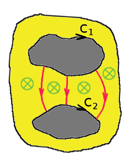
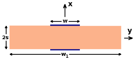
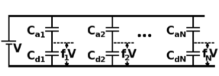
The case of TL in dielectric insulator is much more complicated than the free space case. The fact that the TL propagation wavenumber is different form the free space wavenumber by itself complicates the mathematics (see [4]), but in addition it comes out that one needs to consider in this case polarisation currents in addition to free currents. Hence, to define a generic algorithm for determining the radiation losses for two-conductors TL isolated in dielectric material, one needs a generic specification for the polarisation currents. Given polarisation current elements are summed vectorially (see red lines in Figure 1), so that elements perpendicular to the vector sum do not contribute, one has to define an average relative dielectric permittivity, named (the subscript “p” stands for polarisation), which is smaller or equal to the known equivalent relative dielectric permittivity [7, 8].
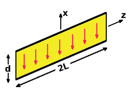
There are three appendices in this work. Appendix A explains some basics on Quasi-TEM cross section behaviour. We discuss the propagation wavenumber , the equivalent relative dielectric permittivity and their connection to the capacitance per length unit and the characteristic impedance (which are strictly speaking well defined only for “pure” TEM). In Appendix B we develop the far potential vector, and similarly to [3], we show that one can represent any two-conductors TL isolated in dielectric material, by a twin lead (see Figure 2), provided the electrical size of the cross section is small.
As mentioned before, we calculate in the appendix also the contribution of the polarisation currents, and those require a generic definition of an average relative dielectric permittivity, . The connection between and and some more insight into their physical meaning is discussed in Appendix C.
The main text is organised as follows. In section II we calculate the power radiated by a TL carrying a forward wave (matched TL), for a general cross section of the TL, as shown in Figure 1. We base the calculations on the results of Appendix B, in which we show (similarly to [3]) that the radiation from a TL of any cross section of small electrical dimensions can be formulated in terms of a twin lead analogue as shown in Figure 2, but unlike in the free space case, this twin lead includes also a sheet of polarisation surface current. After deriving the radiated power and the radiation pattern for the matched TL, we show the limit of the free space case and the limit of a long TL, and how this connects to a semi-infinite TL. The results for the matched TL are generalised for any combination of waves .
In section III, we validate the theoretical results obtained in section II, by comparing them with a previous work dealing with radiation from TL [5]. This work was concerned with reducing radiation losses by using a side plate (mirror) to create opposite image currents, and they considered the free space case, and also TL inside dielectric, but ignored polarisation currents. Reducing our configuration to the assumptions in [5], shows a very good comparison with these results. We then compare our theoretical results with ANSYS-HFSS commercial software simulation results for two cross section examples. The work is ended by some concluding remarks.
Note: through this work, we use RMS values, hence there is no 1/2 in the expressions for power. Partial derivatives are abbreviated, like for example derivative with respect to time .
II Radiated power
II-A Matched TL
We calculate in this section the power radiated from a matched general Quasi-TEM two-conductors TL insulated in a dielectric material of any cross section, as shown in Figure 1, carrying a forward wave described by the current
| (1) |
where . As shown in Appendix B (similarly to [3]), for the purpose of calculating far fields, any general cross section, can be explored by its equivalent twin lead representation shown in Figure 2. The free currents in the TL line conductors and longitudinal ( directed) polarisation currents define the separation distance between the conductors in the twin lead representation (Eq. B.35), and define the component of the far potential vector computed in Eq. (B.45).
The free termination currents of the TL and the transverse polarisation current density, represented by a sheet of directed surface polarisation current density in the twin lead representation define the directed component of the far potential vector computed in Eq. (B.51).
Using these results from Appendix B, we calculate here the total radiated power from the TL. Starting with the contribution of the longitudinal currents, we rewrite Eq. (B.45) in this form
| (2) |
where
| (3) |
and the subscript denotes the contribution from the directed currents, and is the directivity associated with this contribution. To obtain the far fields (those decaying like ), the operator is approximated by and one obtains:
| (4) |
and the electric field associated with it is .
To calculate the contribution of the transverse ( directed currents), we rewrite Eq. (B.51) in this form
| (5) |
where
| (6) |
and the subscript denotes the contribution from the directed currents, and is the directivity associated with this contribution.
The parameter comes from defining the polarisation currents as times the displacement current, and as explained in Appendix C, the ratio represents the average projection factor of the polarisation current elements on the main () axis - the axis with respect to which the twin lead model has been defined (see Figure 2). In cross sections having a transverse E field mainly in the direction the projection factor is close to 1, hence , and in the opposite extreme case (negligible polarisation currents), so that . As evident from Eq. (6), always appears in the ratio , we therefore use the definition
| (7) |
so that
| (8) |
We may therefore use , so that the power satisfies , but as explained in Appendix C, the equality case is not physical, so it is considered only in the context of “ignoring the transverse polarisation”.
To obtain the far fields, we use and the identity , getting
| (9) |
and the electric field associated with it is .
Now summing Eqs. (4) with (9) we obtain the total far magnetic field
| (10) |
and the electric field . We use from here the superscript “+”, because those results are for a forward wave. The Poynting vector is
| (11) |
and the total radiated power is calculated via
| (12) |
We remark that , so that the radiated power is given by the single integral in . After changing variable: , one obtains
| (13) |
The integral is carried out analytically, resulting in an expression which is very big, and therefore we introduce some definitions. We define the following function arguments:
| (14) |
Furthermore, we define
| (15) |
| (16) |
where and are the sine and cosine integral functions respectively. The solution of the part in the integral in Eq. (13), without the prefactor , is given by the function :
| (17) |
and the solution of the part in the integral in Eq. (13), without the prefactor , is given by the function as follows:
| (18) |
So the solution of the whole integral is described by the function
| (19) |
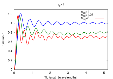
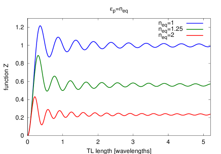
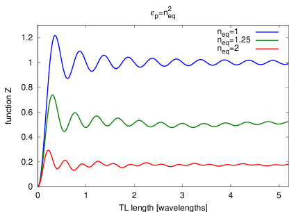
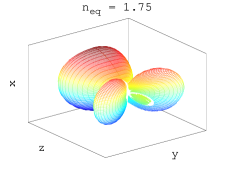
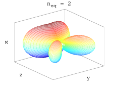
The behaviour of is shown in Figures 3-5 and referred to hereinafter. Looking at the figures, we understand that as is bigger, the function decreases, while for a given , bigger transverse polarisation currents (bigger , hence smaller ), further decrease .
From (13) and (19), the expression for the radiated power is
| (20) |
The radiation pattern function is calculated from the radial pointing vector (Eq. (11)) and the total power in Eq. (20), using which comes out
| (21) |
and the radiated power relative to the forward wave propagating power () is given by
| (22) |
The expressions for the radiated power and radiation pattern are complicated (certainly relative to the free space case [3]) and it would be of interest to compare them to the free space case and determine some limits, in the following subsections.
II-A1 The free space limit
In this limit , and also , according to Eq. (8). So , and in Eq. (19) is , resulting in
| (23) |
We note that
| (24) |
for , so we recover the free space formula for
| (25) |
shown in blue colour in Figures 3-5, see [3]. The limit of the radiation pattern is
| (26) |
which remains only a function of , recovering Eq. (12) in [3].
II-A2 The limit of a long TL
In the free space case the limit for a long TL () is simply . In our case this limit depends on and . For , and both go to . The function goes to 0 for large argument, therefore Eq. (16) reduces to
| (27) |
The function , but here one has to be careful, because we need the limit of in Eqs. (17) and (18). The function for large argument behaves like:
| (28) |
and from here it is easy to find that decreases faster than , hence
| (29) |
also for , we therefore obtain after some algebra the following limit for :
| (30) |
Those limits can be calculated for the cases shown in Figures 3-5 and yield 1, 0.79 and 0.704 for (Figure 3), 1, 0.56 and 0.23 for (Figure 4) and 1, 0.5 and 0.18 for (Figure 5), for the values of , 1.25 and 2, respectively.
II-A3 The limit of big relative dielectric permittivity, for long TL
This limit is discussed in the context of a long TL, so the limit of (30) for depends on , as follows:
| (33) |
so that there is a singular case of “ignoring the transverse polarisation”, for which the limit is 2/3, as shown in Figure 3, and for any practical case the limit is 0, meaning that the radiated power vanishes for strong relative permittivity of the dielectric insulator (see Figures 4 and 5).
II-B Generalisation for non matched TL
We generalise here the result (20) obtained for the losses of a finite TL carrying a forward wave to any combination of waves, as follows:
| (34) |
where is the forward wave phasor current, as used in the previous subsection and is the backward wave phasor current, still defined to the right in the “upper” line in Figure 2.
The solution for the general current is obtained as superposition of the solutions for the fields generated by and . The solution for the backward moving wave , can be found by first solving for a reversed axis in Figure 2, i.e. a axis going to the left, and replacing in the solution (10) , so one obtains
| (35) |
where and are the spherical angles for the reversed axis. Now to express the solution for the backward wave in the original coordinates, defined by the right directed axis, one has to replace: , , and therefore also and , and sum (10) with (35), obtaining
| (36) |
from which the electric field is , so that the Poynting vector is
| (37) |
where we used the abbreviations: and .
We calculate the radiated power using Eq. (12), and obtain
| (38) |
where are the powers radiated by the individual forward and backward waves, and are given by (20), using the adequate current:
| (39) |
and is the power radiated by the interference between and , and is given by
| (40) |
where
| (41) |
The arguments and are defined in Eq. (14) and is defined in Eq. (27).
Unlike the free space case [3] in which , for TL in insulated dielectric the interference between the waves contributes to the radiation, and of course the contribution vanishes in the free space limit for which . To be mentioned that , may also occur in the insulated case () if .
In the next section we validate the analytic results obtained in this section, using ANSYS commercial software simulation and additional published results on radiation losses from TL.
III Validation of the analytic results
III-A Comparison with [5]
In 2006 Nakamura et. al. published the paper “Radiation Characteristics of a Transmission Line with a Side Plate” [5] which intends to reduce radiation losses from TLs using a side plate. The side plate is a perfect conductor put aside the transmission line, to create opposite image currents, and hence reduce the radiation.
The authors first derived the radiation from a TL without the side plate, for the free space case, and also for TL inside dielectric, but the dielectric has been taken into account in what concerns the propagation constant only, ignoring the polarisation currents.
Therefore for the sake of comparison with [5] we have to use , hence in all our results.
We first remark that in [5] is a forward current, and from Eq. (19) in [5], it is evident that they used RMS values. Hence in [5] is the equivalent of our . Also they used (capital) for the equivalent refraction index, called in this work .
In [5] they did not obtain analytic expression for the radiation as function of TL length, but they did obtain analytic expressions for the long TL limit, with which we compare here our results. Eq. (30) simplifies for to:
| (42) |
so that the power radiated by a semi-infinite TL in Eq (32) is:
| (43) |
which is exactly what they called “the radiated power from the input end (or output end) alone”, given in Eq. (30) in [5] (note that they used the distance between conductors , corresponding to our , from there the factor 4).
Also note that the limit of in Eq. (42) for is 2/3, according to the case in Eq. (33). This may be confirmed by comparing Eqs. (31) and (32) in [5].
Next we compare the radiation patterns obtained in Figure 5 of [5], with ours. In [3] we compared the free space case in panel (a), and here we compare our result (Eq. (21) with ) with panel (b) of Figure 5 in [5], showing the radiation patterns for a TL of 1 wavelength, for different values of . This is shown in Figure 6.
It is worthwhile to remark that the radiation pattern (Eq. 21) does not depend on the distance between the conductors (or in [5]), hence the annotation of in Figure 5 of [5] is redundant, and probably has been added to the caption because the authors computed the radiation patterns numerically for , without deriving an analytic expression.
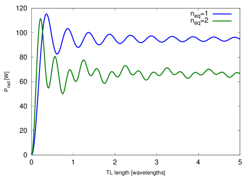
Next, we compare our results with Figure 6 in [5], which is the numerical integration of Eq. 20 in [5] for the cases and 2 (named ,2) where the solid line represents the free space case () and the dashed line represents the case. To calculate the result in Figure 6 of [5] they used A, hence we set A in Eq. (20). is the distance between the conductors in [5], equivalent to in this work, and they used , therefore in Eq. (20). Hence the prefactor [W]. The asymptotic value of in Eq. (42) is 1 for and 0.704 for (as shown also in Figure 3), therefore the asymptotic power for , for the two cases shown in the figure are [W] and [W], respectively. The results of Eq. (20) for and 2 are displayed in Figure 7 (and they are identical in shape to the corresponding cases of and 2 in Figure 3, up to the constant [W]).
III-B Comparison with ANSYS simulation results - Example 1
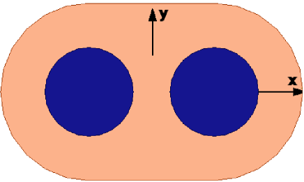
In this example we use the cross section shown in Figure 8, which is similar to the one used in [3], only insulated in a dielectric material.
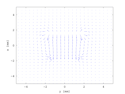
We performed an ANSYS-HFSS cross section analysis at the frequency 240 MHz. From this analysis we obtained the propagation constant [1/m], establishing the equivalent refraction index . An arrow plot of the transverse electric field is shown in Figure 9.
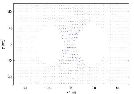
From this analysis, using Eqs. (B.28), (B.31 and (B.32) one finds that , confirming Eq. (B.33) and we obtain the separation distance in the twin lead representation cm (close to the distance obtained in the free space case [3], 2.54 cm).
Next using Eq. (B.44) we obtain , so that . From the cross section analysis we also obtain the value of the characteristic impedance , which is very close to what we obtained in [3] for a similar configuration 105.6 divided by (see Eq. (A.15)). This confirms that the electric size of our cross section is small (see discussion at the end of Appendix A).
We summarise here the parameters used in Eq. (22) for the comparison with simulation:
| (44) |
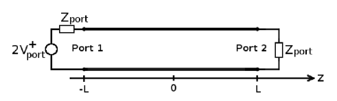
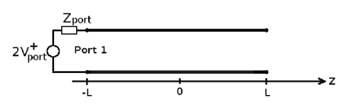
The simulation setup is shown schematically in Figure 10. The TL is ended at both sides by lumped ports of characteristic impedance , but fed only from port 1 by forward wave voltage , so the equivalent Thévenin feeding circuit is a generator of in series with a resistance .
We obtained from the simulation S matrices defined for a characteristic impedance at both ports, for different lengths of the transmission line (similarly to [3]). By symmetry, the S matrix has the form
| (45) |
from which one may calculate the ABCD matrix of the TL [8, 13, 14, 15]. We need only the A element from the ABCD matrix (which is insensitive to the value of ), as follows:
| (46) |
from which we compute the delay angle of the TL
| (47) |
The real part of represents the phase accumulated by a forward wave along the TL, and the imaginary part of (which is always negative) represents the relative decay of the forward wave (voltage or current) due to losses (in our case there are only radiation losses) along the TL, so that . Therefore, the power carried by the forward wave , but for small losses , so that the difference between the input and output values of (which represent the radiated power in Eq. (22)), relative to the (average) power carried by the wave is obtained by
| (48) |
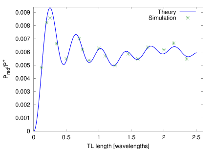
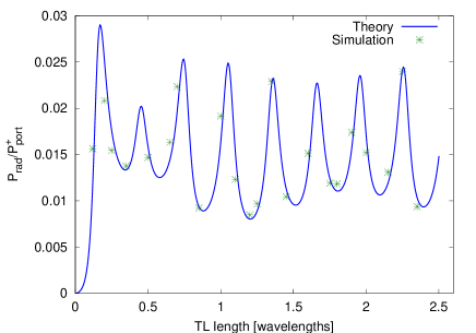
In Figure 11 we compare the analytic result for the relative power radiated by a forward wave in Eq. (22) with the result in Eq. (48) obtained from ANSYS-HFSS simulation, at the frequency 240 MHz.
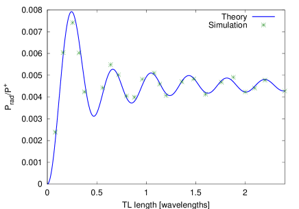
The result shows a very good match between theory and simulation with an average absolute relative error of 4%.
For this cross section is 0.93, hence close to 1, so the interference term (Eq. (40)), which scales like is small. We therefore do not simulate it for this cross section example, and we shall do it in the next example, as follows.
III-C Comparison with ANSYS simulation results - Example 2
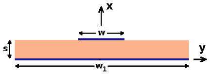
In this example we use a microstrip cross section shown in Figure 12. The width of the “plus” conductor is mm, the distance between the conductors is mm and the relative permittivity is . We avoided the conventional notation for the distance between the conductors, because is reserved for the equivalent distance in the twin lead representation, computed from the cross section analysis (see Appendix B). However, as expected, for the microstrip case it comes out that equals the distance between the conductors, as we shall see in the following cross section analysis.
Using the microstrip formulae [8], we obtain:
| (49) |
so that . The characteristic impedance for is given by (see [8])
| (50) |
Because of the “infinite” ground conductor in the definition of the microstrip, the theoretical solution implies 0 fields in the region , and of course perpendicular E field and parallel H field on the plane . We need to run simulations to determine the fields’ structure in the cross section and to calculate the S parameters for different microstrip lengths, for finding the radiation losses as function of the TL length, as we did in the previous example. Clearly, simulations cannot reproduce fields close to 0 at , unless one chooses a very big value for , consuming a lot of time and memory. For values of of the order of (like or ), simulations on the configuration in Figure 12 will suffer from significant inaccuracy, not being able to assure a perpendicular E field and a parallel H field on the plane .
The method to overcome this is to use an “imaged” configuration shown in Figure 13.
The imaged microstrip configuration assures by symmetry perpendicular E field and parallel H field on the plane , independently of the size of . It appears that increasing above the value almost does not change the results, hence the choice is very good.
We also remark that for a given forward wave current , the imaged configuration carries twice the power of the original configuration, implying a value of characteristic impedance which is twice the value in Eq (50), i.e.
| (51) |
Also, for a given forward wave current , the imaged configuration radiates twice the power of the original configuration, so that the relative radiated power in Eq. (22) is unchanged.
Like in the previous example we perform a cross section analysis, and Figure 14 shows an arrow plot of the transverse electric field .
From the cross section results, using Eqs. (B.28), (B.31) and (B.32), we find that the weight of the longitudinal polarisation is negligible (as in the previous example) and one obtains the separation distance in the twin lead representation mm. As mentioned previously, we expected this separation distance to be equal to the distance between the conductors, and indeed it came out (see Figure 13).
From the cross section analysis we also obtain the value of the characteristic impedance (very close to this in Eq. (51)) and the equivalent dielectric permittivity (very close to this in Eq. (49)), so . Using Eq. (B.44) we obtain , which equals in this case to , so that .
We summarise here the parameters for this cross section:
| (52) |
We first compare with ANSYS-HFSS simulation the power radiated by a forward wave, relative to the power carried by the wave (Eq. 22), following the same procedure described in the previous example, and using the same schematic setup in Figure 10. We obtained S matrices for different TL length and used Eqs. (45)-(48) to elaborate the simulated data. The comparison is shown in Figure 15.
The result shows a very good match between theory and simulation with an average absolute relative error of 3.2%.
For this cross section (far from 1), it is therefore expected the interference term (Eq. (40)) to be substantial. We built a simulation setup shown schematically in Figure 16
to simulate the effect of the interference term. The TL is fed at by a lumped port of with a wave of so the equivalent Thévenin feeding circuit is a generator of in series with a resistance (like in the setup from Figure 10), but the right side at is left open.
Using as first approximation the lossless TL theory, the open end implies , and the following connection between the phases of and
| (53) |
from which
| (54) |
This relation is used in Eq. (40) to calculate the interference term contribution in Eq. (38). The value of (or ) to be used for the terms in Eq. (39), in terms of is given by
| (55) |
Note that the values in Eqs. (54) and (55) are calculated separately for each value of , for the comparison with simulation.
By conservation of energy, the power radiated according to Eq. (38), must be equal to the power of the forward wave coming from port 1: , multiplied by . In Figure 17 we compare the analytic result from Eq. (38) relative to the port power:
| (56) |
with the values of obtained from the ANSYS-HFSS simulation for different TL lengths.
The result shows a very good match between theory and simulation with an average absolute relative error of 1.8%.
IV Conclusions
We presented in this work a general algorithm for the analytic calculation of the radiation losses from transmission lines of two conductors in a dielectric insulator. This work is the generalisation of [3], which deals with TL in free space, and similarly to [3], we assumed a small electric cross section, so that the TL carries a Quasi-TEM mode, which behaves similar to TEM.
We derived the radiation losses of matched TL (carrying a single forward wave) and generalised the result for non matched TL, carrying any combination of forward and backward waves. Unlike in the free space case [3], the interference between the forward and backward wave have a non zero contribution to the radiated power, and we successfully validated our analytic results by comparing them with the results of ANSYS-HFSS simulations for both matched and non matched TL. Also, we compared the matched case with [5], but had to neutralise the polarisation currents for the sake of this comparison (given the fact that that [5] did not include them in their calculation).
For the specification of the transverse polarisation currents we introduced a new definition of , which basically would mean the usual if all the polarisation current elements would be in the same direction (as approximately occurs in a microstrip). However in the general case, , where the relation represents the average projection of the polarisation current elements on the main direction of the resultant contribution (set without loss of generality as the direction).
Appendix A Cross section analysis of Quasi-TEM mode
We perform in this manuscript Quasi-TEM cross sections analyses, to obtain characteristics which affect the radiation process of dielectric insulated TL. We therefore summarise in this appendix some properties of the cross section solution for a general case of hybrid TE-TM fields [7, 8]. The time dependence is , so that the derivative with respect to time of any variable is a multiplication by .
We call the longitudinal ( directed) fields and , and the transverse ( and components) and . The transverse “nabla” operator is named in Cartesian coordinates. One looks for a forward wave solution, having the dependence of the form
| (A.1) |
implying
| (A.2) |
on any variable. This requirement implies the solution of the Helmholtz equations for the longitudinal fields, and linear relations connecting the transverse fields and with and , see [7, 8].
For a guided propagation mode, the longitudinal fields are 90 degrees out of phase relative to the transverse fields, so that any transverse Poynting vector is pure imaginary, which means that there is a standing wave in the transverse direction and the only net energy is flowing in the longitudinal direction [7, 8].
It is therefore convenient to scale the phase of the cross section solution so that the transverse fields are real and the longitudinal fields are pure imaginary, so that:
| (A.3) |
and
| (A.4) |
where the “R” and “I” subscripts indicate real and imaginary parts, respectively. From the cross section solution one obtains the Quasi-TEM mode propagation wavenumber (see Eqs. (A.1) and (A.2)), from which one defines the effective refraction index of the solution via
| (A.5) |
where
| (A.6) |
is the free space wavenumber, being the free space speed of light in vacuum. This equivalent refraction index satisfies , according to “how much” fields are in the dielectric and “how much” in the surrounding air, where is the refraction index of the dielectric material.
To be mentioned that such mode is called Quasi-TEM, because it behaves close to TEM, in the sense that the transverse fields and are dominant relative to the longitudinal fields and . This may be symbolically written as
| (A.7) |
in the averaging sense ( is the free space impedance). As smaller the electrical size of the cross section, the above condition is more accurate.
Now examining the surface free current continuity on one of the conductors in Figure 1 (say the “plus” conductor having the contour ), we obtain
| (A.8) |
where is the free surface charge and and are the longitudinal and transverse components of the free surface current. Using and (Eq. (A.2)), we get
| (A.9) |
Clearly the free transverse surface current which is proportional to is negligible relative to longitudinal surface current which is proportional to (see Eq. (A.7)). But for now we do not need this condition, because the last term in Eq. (A.9) vanishes after integrating around the contour , obtaining
| (A.10) |
where is the charge per longitudinal length unit. We shall use , for the forward current and voltage waves, respectively (we deal with a forward wave, so in principle, all quantities should have a “+” superscript, but it would be too cumbersome). Here we use the capacitance per length unit defined via :
| (A.11) |
and for this we do need condition (A.7), because the potential difference between the conductors has a meaning only if its value is independent of the integration trajectory, and this is strictly correct only if .
Supposing condition (A.7) is satisfied and using Eqs. (A.5), (A.6), and the definition of the characteristic impedance , we obtain
| (A.12) |
and comparing it to the “telegraph model” definition , being the inductance per length unit, one obtains
| (A.13) |
Dealing with dielectric materials, the inductance per unit length is the same as the free space inductance, we therefore conclude from Eq. (A.13) that is proportional to , so that
| (A.14) |
From Eqs. (A.12) and (A.14) it results that is inverse proportional to , so that
| (A.15) |
We may understand from this analysis that the relation between and , namely describes in the DC limit the connection between the capacitance per unit length (or the characteristic impedance) with dielectric and the parallel value in free space according to Eqs. (A.14) and (A.15). Therefore the relation between and keeps linear as long as the electric size of the cross section is small, and may deviate from this relation for higher frequencies.
Appendix B Far vector potential of separated two-conductors transmission line in twin lead representation
In this appendix we calculate the far magnetic vector potential for a general TL insulated in a dielectric material of relative dielectric permittivity as shown in Figure 1.
In spite of dealing with dielectric insulators on has to use the regular free space Lorenz gauge [6], in the frequency domain
| (B.1) |
obtaining the following wave equations for the magnetic vector potential and the scalar potential [6]:
| (B.2) |
| (B.3) |
where
| (B.4) |
| (B.5) |
and being the free current and charge densities, respectively,
| (B.6) |
is the electric polarisation field and
| (B.7) |
is the magnetisation field which is 0 in our case.
We remark that and satisfy the continuity equation
| (B.8) |
(which holds separately for the free and polarisation charges/currents). We see that can be calculated from , the same as can be calculated from using (B.1). This means that we have to solve only Eq. (B.2), as usually done in radiation problems [7, 9, 10, 11, 12]. Its formal solution, for a TL from to is the convolution integral
| (B.9) |
where
| (B.10) |
is the 3D Green’s function and
| (B.11) |
We remark that (B.9) is the potential vector due to the currents along the TL, and the contribution of the termination (source and load) currents [3] are calculated at the end of this appendix.
According to (A.1), we use
| (B.12) |
and approximating in (B.11) in far field in spherical coordinates to
| (B.13) |
we rewrite in the far field
| (B.14) |
At this point the integral can be separated from the cross section integral. Integrating on we obtain
| (B.15) |
where and is
| (B.16) |
so that the direction of is according to the direction of .
Considering the higher modes to be in deep cutoff, so that (small electric cross section), and defining the radial cross section unit vector
| (B.17) |
and the radial cross section integration variables vector
| (B.18) |
we may rewrite Eq. (B.16) as
| (B.19) |
The strategy to calculate is as follows: for components of on which the integral vanishes over the TL cross section, we perform the integral of the component multiplied by , as follows
| (B.20) |
while for components of on which the integral is not 0, we neglect relative to 1, as follows
| (B.21) |
For the free space TL [3] we had to deal only with the longitudinal ( component) of in what concerns the TL currents contribution (which were free surface currents in the direction), and we had transverse components ( or ) of only from the terminations of the TL. In the current case we note that contains both free longitudinal surface currents and polarisation currents contributions (which have both longitudinal and transverse components). We therefore deal first with the longitudinal component of , which is written as:
| (B.22) |
where is the contribution of the longitudinal free surface currents and hence is similar to [3] (so that the solution to Eq. (B.19) has the form (B.20)):
| (B.23) |
where is the contour parameter around the perfect conductors (i.e. and , see Figure 1). Separating the contours and noting that we deal with a differential mode for which the currents in the conductors are equal but with opposite signs, and using (i.e. the component of parallel to the conductors) one obtains:
| (B.24) |
the forward current is
| (B.25) |
| (B.26) |
The vector represents the vector distance pointing from the “negative” conductor to the “positive” conductor in the twin lead equivalent (see Figure 2). As in [3] it is convenient to redefine the axis to be aligned with , so that and , so that (B.24) simplifies to
| (B.27) |
and the expression for the distance simplifies to
| (B.28) |
For in Eq. (B.22) we use the longitudinal polarisation current density (see Figure 1), which according to (A.4) can be written as , and the integration is only on the dielectric region. Clearly, being a solution of the Helmholtz equation, the integral on the TL cross section vanishes, and for the twin lead representation, we obtain
| (B.29) |
which can be written as
| (B.30) |
where
| (B.31) |
and represents the Heaviside step function, limiting the integral to the regions in which and
| (B.32) |
Clearly, being the ratio between something proportional to and , which is proportional to , satisfies
| (B.33) |
(see Eq. (A.7)). Using the above definitions, we sum Eqs. (B.27) and (B.30) to obtain the total component of
| (B.34) |
where
| (B.35) |
is the separation distance between the conductors in the twin lead representation, analogous to what we obtained in [3]. For the case of conductors in dielectric insulator this vector separation has two contributions: is due to the free currents, due to the polarisation currents and is the “weight” of the longitudinal polarisation contribution, but as explained above, this weight is typically small (see Eq. (B.33)).
Now we calculate the transverse component of , which under the twin lead representation simplifies to (see Figure 2), where is due to the transverse polarisation currents. We therefore use for the directed polarisation current density (and the solution to Eq. (B.19) has the form (B.21)):
| (B.36) |
where
| (B.37) |
and is the component of .
It is useful to describe the transverse polarisation current in the twin lead representation as a directed surface current on the surface (see Figure 2). The polarisation (surface) current is proportional to the displacement surface current:
| (B.38) |
where the minus is due to the fact that the current is in the direction. Using relations (A.5) and (A.12), this can be written
| (B.39) |
Inside a uniform dielectric material the polarisation current is times the displacement current, but having part of the fields is in air, it looks like one has to use times the displacement current. As shown in Appendix C, due to the fact that parts of the polarisation current elements are in the perpendicular () direction, if one wants to use the same value for as defined in Eq. (B.35), one needs to use a value for the relative dielectric permittivity in general smaller than , which we name (the subscript “p” stands for polarisation), for expressing the polarisation surface current:
| (B.40) |
and being a surface current on , one gets the polarisation current density
| (B.41) |
The value of satisfies:
| (B.42) |
and Appendix C is dedicated to explain this connection, the physical meaning of and its relation to .
Using (B.41) in (B.36), the integral is carried out from 0 to , while the integral yield 1, because of the delta function, obtaining
| (B.43) |
By comparing (B.43) with (B.36) and using (B.37), one obtains an equation to calculate from the numerical cross section solution, as follows:
| (B.44) |
where the RHS is positive, because the phase of is scaled to point mainly from the “positive” to the “negative” conductor, i.e. it is mainly negative.
At this point we summarise the results for the vector potential components contributed by the currents along the TL. From (B.15) and (B.34) we obtain
| (B.45) |
and from (B.15) and (B.43) we get the directed contribution. Given this contribution is from transverse polarisation, we name it :
| (B.46) |
It is worthwhile to mention that any representation that keeps the value of correct, for example replacing by , but accordingly use a smaller value of for the transverse polarisation would be a completely equivalent representation, but we chose to keep the same value of for representing the free currents and the polarisation currents (see discussion in Appendix C).
Now we calculate the contribution of the termination currents to the potential vector. The twin lead geometry allows us to use a simple model for the termination currents, which are in the direction (see Figure 2), and their values are at the locations respectively. They result in
| (B.47) |
where the indices 1,2 denote the contributions from the termination currents at , respectively, (see Figure 2). The distances of the far observer from the terminations may be expressed in spherical coordinates, as follows:
| (B.48) |
The integral (B.47) is carried out for , using (A.5), results in
| (B.49) |
The two contributions sum to :
| (B.50) |
and we call it , because the termination currents are free currents. The total transverse directed potential vector is obtained by summing (B.46) with (B.50):
| (B.51) |
Appendix C The physical meaning of , and the connection between them
We used in this work a new quantity called for the purpose of defining the contribution of the transverse polarisation currents. This appendix is dedicated to explain the physical meaning of and show the connection between it and .
First, it should be mentioned that it is not the polarisation current per se which affects the radiation, but rather the polarisation current element, i.e. - see Eq. (B.43). Looking at Eq. (B.44), it is clear that the value of is only a function of the cross section geometry (while is something that we defined in Eq. (B.35) to formulate the twin lead model).
This means that the only requirement to obtain a correct expression for the radiation is to use the correct value of , and we had the freedom to replace by and determine accordingly a new value for the equivalent distance for the polarisation contribution and call it for example. This would imply
| (C.1) |
so the usage of and gives a completely equivalent formulation, leading to the same result. The only reason we did not choose it is aesthetic: we simply preferred a uniform twin lead model for both free currents and polarisation, having the same effective separation distance .
We emphasise this point, because we need a consistent definition for the separation distance to analyse the polarisation current elements in an equivalent circuit that we develop here (shown in Figure C.1).
For this purpose we use the same value used along the whole paper, i.e. this one given in Eq. (B.35).
We consider the capacitors in Figure C.1 as parallel plates capacitors, as follows
| (C.2) |
where is a fixed effective area (more accurately perpendicular length), and are the effective separation distances of the air and dielectric parts, respectively, and we require their sum to be the total effective separation distance mentioned before:
| (C.3) |
From Eqs. (C.2) and (C.3) it is easy to show that and come out
| (C.4) |
and the capacitor may be written as
| (C.5) |
The field lines describing the capacitors in the equivalent circuit in Figure C.1 are shown in Figure C.2 for a microstrip.
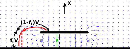
In general each field line is partly in the air and partly in the dielectric, so that the voltage on the air is and the voltage on the dielectric is . According to this, we defined the fraction of voltage on the dielectric, as evidently shown on the “red” line in Figure C.2. The “green” line in Figure C.2 passes only through the dielectric, it is therefore a special case of the above with . The dashed “red” line shows the projection of the continuous line (inside the dielectric) on the direction, and the relation between the projected line and the original line is called for the electric field line . For the red line, is not equal, but close to 1. For the green line, being in the direction, . The projection is discussed further on in context with the polarisation currents.
Given the number of capacitors is , the total capacitance per longitudinal unit length is equal the sum on of all the capacitances in Eq. (C.5)
| (C.6) |
The free space capacitance is obtained by setting all : , and the value of is calculated from Eq. (A.14), obtaining
| (C.7) |
or in a more suggestive form:
| (C.8) |
where is the average fraction of voltage on the dielectric. Given that electric field is proportional to voltage, and polarisation vector is proportional to times electric field (see Eq. (B.6)), suggests that indicates on the average polarisation vector. We remark that using Eqs. (C.6) and (C.7), one can write the total capacitance as
| (C.9) |
so that it is represented by a parallel plates capacitor of relative dielectric permittivity , distance between the plates and area (or rather perpendicular length) .
Now we calculate the polarisation current element. On a given capacitor, the displacement current is , which is also the (AC) current passing through the capacitor. We remark that this total current is a cross section integral on a current density vector in the space between the plates, and this vector may have different directions in different locations. The total effect on the radiation comes from the equivalent polarisation current element vector contribution (we chose the axis in this direction - see Appendix B). We therefore need the projection of the polarisation current element vector (see projection factor - dashed red line in Figure C.2) - we shall call it . It is obtained by multiplying by , where already includes effect of the projection, as explained at the beginning of this appendix. Considering the parallel plate capacitor of our model in Eq. (C.9), we have
| (C.10) |
Now we apply this to our model: the total polarisation current element is the sum on the polarisation current elements on all the capacitors in dielectric . The contribution from each capacitor is times the voltage on this capacitor , times the projection factor , times , hence we obtain
| (C.11) |
Now comparing (C.10) with (C.11), yields
| (C.12) |
We divide it by from Eq. (C.8), obtaining
| (C.13) |
or in a more suggestive form:
| (C.14) |
where is the projection factor averaged by the fraction of voltage in the dielectric. Given that , also
| (C.15) |
and hence
| (C.16) |
however it seems that cannot be 0 for a physical system, hence the lower limit should be bigger than 0, so that practically always. Hence we consider the case of , or only in the context of “ignoring the transverse polarisation”. For the microstrip example (see Figure 14), , so that , but for the circular shaped conductors cross section (see Figure 9), .
Using this model, we can also show that the solution of Eq. (B.44) yields (C.14). The integral in Eq. (B.44), carried over the dielectric region, yields on capacitor , , and this is summed on all capacitors:
| (C.17) |
Using , Eq. (A.12), and , one obtains
| (C.18) |
and using from Eq. (C.9), reproduces exactly Eq. (C.12), leading to the result (C.14).
Returning to the discussion at the beginning of this appendix (from which we derived Eq. (C.1)), we understand from Eq. (C.14) that the physical meaning of is expressed by the relation
| (C.19) |
so that in the representation we used in this work of keeping the separation value , the projection factor lies in the definition of . In the alternative representation of replacing by and use for the effective separation the value , the projection lies in the separation .
References
- [1] R. Ianconescu and V. Vulfin, TEM Transmission line radiation losses analysis, Proceedings of the 46th European Microwave Conference, EuMW 2016, London, October 3-7 (2016)
- [2] R. Ianconescu and V. Vulfin, Simulation and theory of TEM transmission lines radiation losses, ICSEE International Conference on the Science of Electrical Engineering, Eilat, Israel, November 16-18 (2016)
- [3] R. Ianconescu and V. Vulfin, Free space TEM transmission lines radiation losses model, arXiv:1701.04878 (2016)
- [4] R. Ianconescu, and V. Vladimir, ”Quasi-TEM insulated transmission line radiation losses analysis.” Microwaves, Antennas, Communications and Electronic Systems (COMCAS), 2017 IEEE International Conference on. IEEE, 2017.
- [5] T. Nakamura, N. Takase and R, Sato, Radiation Characteristics of a Transmission Line with a Side Plate, Electronics and Communications in Japan, Part 1, Vol. 89, No. 6, 2006
- [6] U. Krey, A. Owen, Basic Theoretical Physics – A Concise Overview, Berlin-Heidelberg-New York, Springer 2007
- [7] Orfanidis S.J., Electromagnetic Waves and Antennas, ISBN: 0130938556, (Rutgers University, 2002)
- [8] D. M. Pozar, Microwave Engineering, Wiley India Pvt., 2009
- [9] S. Ramo, J. R. Whinnery and T. Van Duzer, Fields and Waves in Communication Electronics, 3rd edition, Wiley 1994
- [10] E. C. Jordan and K. G. Balmain, Electromagnetic Waves and Radiating Systems, 2nd edition, Prentice Hall 1968
- [11] C. A. Balanis, Antenna Theory: Analysis and Design, 3rd edition, John Wiley & Sons, 2005
- [12] W. L. Stutzman and G. A. Thiele, Antenna Theory and Design, 3rd Edition, John Wiley & Sons, 2012
- [13] V. Vulfin and R. Ianconescu, Transmission of the maximum number of signals through a Multi-Conductor transmission line without crosstalk or return loss: theory and simulation, IET MICROW ANTENNA P, 9(13), pp. 1444-1452 (2015)
- [14] R. Ianconescu and V. Vulfin, Analysis of lossy multiconductor transmission lines and application of a crosstalk canceling algorithm, IET MICROW ANTENNA P, 11(3), pp. 394-401 (2016)
- [15] R. Ianconescu and V. Vulfin, “Simulation for a Crosstalk Avoiding Algorithm in Multi-Conductor Communication”, 2014 IEEE 28-th Convention of Electrical and Electronics Engineers in Israel, Eilat, December 3-5