Graphene Labs, Istituto Italiano di Tecnologia, Via Morego 30, I-16163 Genova, Italy \alsoaffiliationGraphene Labs, Istituto Italiano di Tecnologia, Via Morego 30, I-16163 Genova, Italy \alsoaffiliationCNR NANOTEC-Istituto di Nanotecnologia, Polo di Nanotecnologia c/o Campus Ecotekne, via Monteroni, 73100 Lecce, Italy \alsoaffiliationGraphene Labs, Istituto Italiano di Tecnologia, Via Morego 30, I-16163 Genova, Italy \alsoaffiliationGraphene Labs, Istituto Italiano di Tecnologia, Via Morego 30, I-16163 Genova, Italy
UV Light Detection from CdS Nanocrystal Sensitized Graphene Photodetectors at kHz Frequencies
Abstract
We have fabricated UV-sensitive photodetectors based on colloidal CdS nanocrystals and graphene. The nanocrystals act as a sensitizer layer that improves light harvesting leading to high responsivity of the detector. Despite the slow relaxation of the photogenerated charges in the nanocrystal film, faster processes allowed to detect pulses up to a repetition rate of 2 kHz. We have performed time-resolved analysis of the processes occurring in our hybrid system, and discuss possible photo-induced charge transfer mechanisms.111This document is the Accepted Manuscript version of a Published Work that appeared in final form in The Journal of Physical Chemistry C, 119, 42, 23859, copyright 2015 © American Chemical Society after peer review and technical editing by the publisher. To access the final edited and published work see http://pubsdc3.acs.org/articlesonrequest/AOR-UT8wHWPSqtQ72WdMmjhm
1 Introduction
Graphene has established itself as a platform for electronics and optoelectronics because of its particular properties and versatility.1, 2, 3, 4 It has been exploited for photodetection, operating in a wide range of wavelengths. Here the main advantage of graphene is the intrinsically broad band and tunable absorption, which however yields only very low signal, and therefore limits the performance of pure graphene photodetectors 4.
Recently, hybrid systems composed by graphene and a sensitizer layer have proved to be a promising solution to this limitation, for example with bulk semiconductors, 5, 6 molecules, 7 plasmonic structures, 8, 9 and colloidal semiconductor nanocrystals (NC). 10, 11, 12 In particular colloidal semiconductor nanocrystals are an attractive alternative due to their strong optical absorption that can be tuned via size and composition over a wide spectral range,13 which in turn leads to high responsivity of the hybrid detectors. Furthermore, the nanocrystal layer can be deposited by low cost solution processes. 11, 12, 14 Here the working principle is that of a photoconductor: light is efficiently absorbed by the nanocrystal layer, generating electron-hole pairs. While carriers of one type (e.g., holes) are trapped in the nanocrystals, carriers of the other type (e.g., electrons) are transferred to graphene. The ratio of the relaxation time of the photogenerated charges to the transit time in the graphene channel can result in a large photoconductive gain. However, so far slow recombination processes limit the working speed of such devices below hundred Hz. 4
Investigating the charge dynamics and the transfer mechanisms between the graphene and the nanocrystal layers is therefore important to improve the performance of the devices and to understand the fundamental limits. Previous works have focused on the effect of molecules absorbed onto nanocrystal surface, 15, 16 and highlighted the role of ligands on the surface of nanocrystals.17
In this work, we fabricated photodetectors based on colloidal CdS nanocrystal and CVD graphene from which we achieved high responsivity, fast detection in the kHz range and UV sensitivity. Pulsed laser illumination allows us to access the relevant time scales, and we propose a tentative description of the processes involved in the photoresponse.
2 Experimental
2.1 Graphene growth and device fabrication
The graphene was grown on 25 m-thick Cu foil using low-pressure chemical vapor deposition (CVD). 18 Initially, the foil was electropolished to remove surface impurities and reduce the surface roughness. It was then annealed for 10 minutes at 1060∘C and a pressure of 25 mBar in Ar atmosphere to increase the Cu grain size. The growth of graphene was performed at 1060∘C by flowing 1 sccm of methane, 20 sccm of hydrogen and 980 sccm of argon for 10 minutes, producing isolated single-crystals of graphene of approximately 150 m in diameter The sample was then cooled to 120∘C before removing it from the reactor.
The graphene was transferred using the standard wet transfer technique. The foil was spin-coated with a 200 nm layer of poly(methyl-methacrylate) (PMMA) and immersed for 16 hours in a 0.1 M solution of to etch the copper. After the etching, a film of graphene and PMMA was left floating on the surface of the etchant solution. The film was thoroughly rinsed by transferring it to a beaker of deionized water several times. The target substrate ( chip, 285 nm oxide thickness) was then immersed in the water and the graphene/PMMA film was scooped out of the beaker. The substrate was left to dry under ambient conditions for 60 minutes. Finally, the substrate was immersed in acetone for 4 hours to remove the PMMA support film and rinsed in isopropyl alcohol.
On these samples FETs have been fabricated using electron beam lithography; ohmic contacts (source and drain) were defined by evaporation of Cr/Au (5 nm/40 nm) and lift-off; devices were isolated by reactive ion etching in . Width and length of the channel of the FETs described in this work are m and m. The p-doped silicon substrate was contacted with indium to function as a planar back gate.
2.2 Synthesis of CdS nanocrystals, ligand exchange and thin film deposition
CdS nanocrystals with 3 nm diameter were synthesized following a protocol from Yu and Peng. 19 Briefly, 130 mg CdO, 63 ml octadecene and 4.35 ml oleic acid were mixed in a flask and the flask was connected to a Schlenk line. The mixture was heated to ca. 120∘C under vacuum, and kept at that temperature for 30 minutes. Several purging cycles of nitrogen and vacuum were executed, and finally the flask was heated to 300∘C (under nitrogen) until the solution turned colorless. At that point the flask was cooled to 100∘C and vacuum was applied again in order to remove residual water that formed during the decomposition of CdO. When no more fog was formed in the flask, the flask was filled with nitrogen again and the solution was heated to 293∘C. At that point a solution of sulfur (24 mg) in degassed octadecene (15 ml) was injected into the flask. The temperature control was set to 250∘C after the injection. After 330 seconds, the growth of the nanocrystals was stopped by removing the heat source. Residual organic material was removed from the solution by repeated precipitation of the nanocrystals with methanol and redispersion in toluene.
For the deposition of the films the nanocrystals, the surface of the as-synthesized nanocrystals was chemically modified with p-methylbenzenethiolate ligands replacing native oleate ligands.20. The nanocrystal were passivated with methylbenzenethiol and transferred into a mixture of chloroform and dichlorobenzene (2:3 volume ratio).20, 21 In details, this ligand exchange was performed by adding a methylbenzenethiol solution (95 mg methylbenzenethiol, 10 ml dichlorobenzene, 300 l trioctylamine) in a 2:1 volume ratio to a 300 M solution of CdS nanocrystals in toluene (concentration determined according to Ref. 22). The success of the ligand exchange could be observed by a slight color change of the solution due to the decrease in exciton confinement caused by the methylbenzenethiol ligands.20 The nanocrystals were precipitated by the addition of hexane (ca. 1 ml per 100 l of CdS solution) and redissolved in the solution of methylbenzenethiol. This process was repeated twice. Finally, the nanocrystals were dissolved in the mixture of chloroform and dichlorobenzene.
The thin films on the graphene devices were produced by covering first the substrate with the ligand-exchanged solution of CdS nanocrystals. The substrate with the solution was then covered with a small beaker for 10 minutes. After that, the beaker was removed and the substrate was spun at 300 RPM for 10 seconds and then at 1200 RPM and 2000 RPM for at least 15 minutes until the solvent had evaporated completely.
This procedure yields a 50 nm-thick sensitizer layer covering the conductive graphene channel. A scheme of the final configuration of the device is reported in panel (a) of Fig. 1; panel (b) is false color optical microscope image of one of the investigated devices.
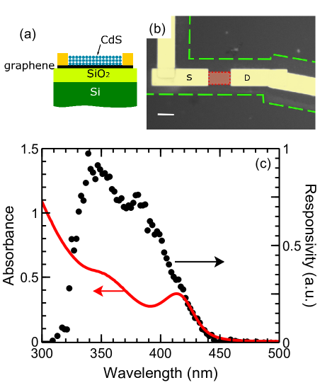
Figure 1c reports the absorbance of the nanocrystals recorded from toluene solution, and the spectral response of a NC coated graphene FET after the UV treatment that is described in detail in the following. The photocurrent spectra corresponds well to the optical absorption of the nanocrystals and confirms their key role in photo carrier generation.
3 Results and discussion
We measured the source-drain resistance as a function of the gate voltage at the different steps of the device fabrication and report the corresponding transfer characteristic in Fig. 2a. All measurements were performed in vacuum.
After transfer and electrode fabrication the graphene is strongly p-doped (curve 1 in Fig. 2a); similar p-doping was found after nanocrystal deposition (curve 2). We then used a pulsed diode laser at 349 nm to illuminate the devices. Curve 3 in Fig. 2a demonstrates that after illumination with the UV light (nanoseconds pulses at 1 kHz leading to an average intensity of 19.8 mW cm-2) the graphene changed to n-doped. We explore this process in more detail in Fig. 2c, where we report the source-drain current measured during this UV-treatment. At the beginning, the sample is in the dark. As the laser is turned on, the current decreases (negative photocurrent) and reaches a minimum value in about 20 s (see inset of Fig. 2b), then the current increases and exceeds the value of the initial dark current, and eventually saturates after about 15 minutes. After passing through the minimum the photocurrent is positive, as shown at and , and the Dirac peak has shifted to negative gate voltage (curve 3 in Fig. 2a), which corresponds to n-doping. This n-doping is stable, and lasts as long as the sample is kept in vacuum.
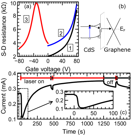
The change from p- to n-doping and the related switching of the photocurrent polarity can be understood in terms of initial oxygen passivation of the NC surface. 23, 15, 16 At the beginning, the nanocrystals have oxygen adsorbed on their surface which can desorb under UV illumination, leaving positively charged surface traps behind, that we assume to be unpassivated atoms. During this process, photogenerated electrons will screen the positive surface traps and at the same time the traps can mediate electron transport into the graphene (see a sketch of the process in Fig. 2b). This process raises the Fermi level in graphene, approaching the Dirac point and thus first reducing the hole conductivity, and after crossing the Dirac point (minimum in Fig. 2c) conduction is mediated by electrons and increases with illumination until the electron transfer saturates. When light is turned off under this condition, the electron density in graphene decreases, photocurrent is positive, and the surface traps on the NC surface cannot efficiently be passivated under vacuum. Thus, the graphene layer does not return to its original p-doped status when the light is turned off, but remains n-doped. Exposing the sample to air restores the original p-doping.
3.1 Photoresponse measurements
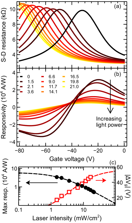
The source-drain resistance as a function of the gate voltage is reported in Fig. 3a, acquired in dark and with increasing laser intensity. Upon UV-treatment, the graphene in the dark is n-doped; the mobility and the residual carrier density are cm2 V-1 s-1 and cm-2, respectively, calculated using the formula in Ref. 24. As the laser power increases, the peak (Dirac point) shifts toward more negative voltage, indicating that electrons are transferred from the nanocrystals. and do not change (within 10%) with illumination.
Fig. 3b shows the responsivity, defined as ( being the power impinging on the device), as a function of the gate voltage. As the gate voltage is swept toward negative values, the photocurrent (hence the responsivity) is positive and reaches a maximum. Then it goes to zero and changes sign reaching a minimum (negative) value and then again approaches zero.
We can model the source drain resistance versus gate voltage by: 24
| (1) |
where is the contact resistance, is the carrier density induced by the gate voltage ( being the gate capacitance per unit area, the Dirac voltage), the residual carrier density, and ( being the mobility, and , being width and length of the FET channel).
The effect of the light is to transfer charge to the graphene. Therefore, we model it replacing , or .
With these definitions, the photocurrent reads
| (2) |
The zero of the photocurrent occurs when , independently of the other parameters. We experimentally observe this dependence on the photogenerated carrier density as the shift in the zero of the responsivity. We can also account for our observation that the photocurrent (and thus the responsivity) approaches zero far away from the Dirac point (large ). In this case, the responsivity is limited by the contact resistance , and one finds
| (3) |
while, if , the photocurrent approaches a constant value
| (4) |
Figure 3b shows a clear impact of Rc since far away from the maximum it approaches zero. However, in order to find a simple expression to fit the maximum of the responsivity in Fig. 3b versus light power, we take , which is justified since it plays only a role far away from the maximum. Furthermore, we need to elaborate on the light power dependence of the photoexcited charges () in the graphene channel.
In general, the number of charge excited in the nanocrystals per unit area is
| (5) |
where is excitation efficiency (including the absorption coefficient), is the power impinging on the device, the lifetime of excited carrier. The charges induced in the graphene layer are given by , where is introduced to account for non-perfect efficiency in the process.
In Fig. 3c we report the dependence of the maximum responsivity and the shift of the Dirac point (that is proportional to ) versus light intensity. In the simplest case the photogenerated charges are directly proportional to the light power. However, in our data we find non-linear behavior, indeed, we observe that the responsivity decreases as the power increases, while with a linear dependence one would expect a constant responsivity following the photocurrent dependence on : , .
Another approach used by other groups is a simple power law (),12, 25 but also this does not reproduce our data. Ref. 15 proposes to explain the saturating behavior of the responsivity based on a power-dependent lifetime of the photogenerated charges, given by
| (6) |
For low power, the lifetime saturates to a finite value . Here describes the dependence at high power. A similar formula was considered also in Ref. 11, with , which worked also for experimental data fits in Ref. 15. In our case, we can fit the power dependence of the responsivity in Fig. 3c using Eq. 3, 5 and 6 with , with the formula
| (7) |
where is the transit time of the carriers in the FET channel. The Dirac point shift is given by
| (8) |
We note that this model was proposed to describe the saturation of trap states on nanocrystal surfaces by photoexcited carriers, which is in line with the processes that we assume relevant for our system.
As for the figures of merit of these devices, the responsivity has a peak value of A/W at 1.5 mW/cm2, and from this value the external quantum efficiency can be evaluated as , reaching . UV sensitivity of our device is demonstrated by a 25-times smaller responsivity in the visible range (measured at 473 nm). With respect to previously reported works, we note that devices of similar concept, based on simple deposition of colloidal nanocrystals, have reached A W-1 in the near UV-blue range,26, 15, 27 with a time response that was of the order of seconds or fractions of seconds, while higher responsivity values can be reached with subsequent chemical process or more complex substrate structures.28, 29
The noise equivalent power (NEP) is given by the current noise divided by the responsivity. The noise can be evaluated experimentally from a time trace of the dark current. This yields 10-12 W Hz-1/2 as minimum NEP at the maximum responsivity, which corresponds to a detectivity (defined as , where is the surface of the device) of 109 Jones. We note, however, that this estimation includes both the intrinsic noise of the device and the noise in the experimental set-up, which was not optimized for such purposes. If we assume only thermal noise, we can estimate the noise current as , being resistance in the dark, the temperature. With this estimate, NEP and detectivity improve to 10-17 W Hz-1/2 and 1013 Jones, respectively.
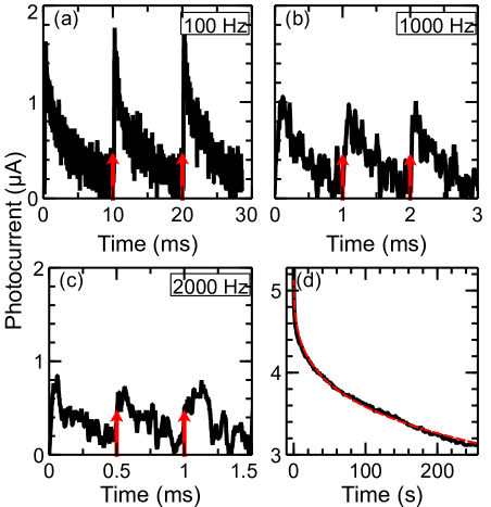
To assess the temporal response of our photodetectors experimentally, we have performed pulsed laser excitation experiments at different frequencies and with varying fluences. Pulse width was some nanoseconds. Figure 4a-c shows time traces of the photocurrent for pulsed stimulation at different frequencies, which clearly demonstrate that the device can detect the laser signal up to 2 kHz (Fig. 4c), which is at least one order of magnitude faster than the values reported for sensitized graphene photodetectors, 11, 15, 17 and several orders of magnitude faster than NC based photodetectors.30 From the fitting of the data in Fig. 3c we can extract a response time of our system in the form of the product , yielding ms for the responsivity fit, and ms for the fit of the Dirac point shift. At least for the fastest response of our detectors these values appear to be in the correct range. We note that will be smaller than 1, thus our fitting represents a lower limit for the charge carrier relaxation time .
Figure 4d reports the time trace of the photocurrent after illumination is turned off on a longer time period. In this case, we observe a much longer timescale for the decay, which we can describe as a persistent photocurrent effect. A simple exponential decay does not reproduce the experimental curve, since the current decay is characterized by an initial fast decrease, followed by a much slower tail. Although a sum of two exponential functions would improve the fit, we can as well use the stretched exponential function , often used to describe the time response in detectors based on nanocrystals and other materials.31, 32, 33 A system described by this formula can be interpreted as a continuous distribution of time scales which sum up in the response.34 Within this model, we obtain the best fit with an average timescale of about 2000 s.
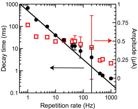
To gain more insight into the time constants that play a role in our system we analyzed the photocurrent time traces at different repetition rate while keeping pulse power, and constant. The time traces were fitted with a single exponential adjusting the amplitude, the decay time and the base current, and the results are reported in Fig. 5. We note that single exponential fits worked well at high frequencies, while at lower frequency (5 Hz) they only described the fastest component of the trace. The good single exponential fits at high frequency are possible because the slower processes contribute only as a DC offset (a persistent photocurrent). Figure 5 shows that the decay time is inversely proportional to the repetition rate and suggests a continuous distribution of time scale . Consistently, the amplitude does not show the typical relation expected for a simple single relaxation time system.
It is well known that the optoelectronic properties of colloidal nanocrystals depend significantly on their surface chemistry.13 While ligands coming from the synthetic procedures result in good surface passivation and colloidal stability in solution, they are detrimental for charge transport. We exchanged these native ligands and worked with methylbenzenethiolate-capped nanocrystals in our devices that yield thin-films with enhanced conductivity.21
With such short ligands the nanocrystal surface becomes more accessible for the photogenerated charges, and shallow surface traps will play a strong role concerning recombination processes. On the other hand, the UV assisted desorption of oxygen molecules under vacuum is likely to result in unpassivated atoms on the NC surface, which should lead to deep trap states approximately 0.7 eV below the conduction band.35, 36, 37
Konstantatos et al.30 have reported that trap states significantly influence the relaxation times of photogenerated carriers in NC films. They demonstrated that deep traps around 0.3 eV below the conduction band lead to long relaxation times of few seconds, while shallow traps of less than 0.1 eV resulted in short times responses of few tens of milliseconds. Consequently, trap state engineering could be exploited as a means to reduce the response time of PbS NC photodetectors to 25 ms by using ethanethiols as surface ligands.38 We therefore tentatively assign the large distribution of relaxation times observed from our hybrid graphene-NC photodetectors to surface trap states with different depth. Here the shallow trap states enable the extremely fast response times of less than a millisecond, while deep traps are responsible for the observed persistent photoconductivity.
4 Conclusions
We presented semiconductor nanocrystal sensitized graphene photodetectors that can provide high sensitivity up to and fast signal detection reaching the kHz range. Here the overcoating of graphene FETs with a layer of CdS nanocrystals by simple spin coating greatly enhanced their absorption in the UV spectral range. The surface passivation of the nanocrystals with methylbenzenethiolate ligands resulted in a photocurrent decay spanning timescales from hundreds of microseconds to minutes.
The fast decay times enabled detection at high repetition rates well above the limit needed, for example, for video recording. This approach can be extended straightforwardly to constitute a platform of semiconductor nanocrystals passivated with arenethiolate ligands, such as Cd-, Pb-, and Zn-based chalcogenides, that enables tuning of the spectral sensitivity of such hybrid photodetectors via the nanocrystal material, while maintaining high sensitivity and fast response. Future developments will aim at increasing the responsivity at high repetition rate by eliminating deep surface traps, and by the use of less toxic nanocrystal materials based on copper indium (gallium) selenides, for instance.
This work was supported by the EC under the Graphene Flagship program (contract no. CNECT-ICT-604391).
References
- Das Sarma et al. 2011 Das Sarma, S.; Adam, S.; Hwang, E. H.; Rossi, E. Electronic transport in two-dimensional graphene. Rev. Mod. Phys. 2011, 83, 407–470
- Avouris 2010 Avouris, P. Graphene: Electronic and photonic properties and devices. Nano Lett. 2010, 10, 4285–4294
- Fiori et al. 2014 Fiori, G.; Bonaccorso, F.; Iannaccone, G.; Palacios, T.; Neumaier, D.; Seabaugh, A.; Banerjee, S. K.; Colombo, L. Electronics based on two-dimensional materials. Nat. Nanotechnol. 2014, 9, 768–779
- Koppens et al. 2014 Koppens, F. H. L.; Mueller, T.; Avouris, P.; Ferrari, A. C.; Vitiello, M. S.; Polini, M. Photodetectors based on graphene, other two-dimensional materials and hybrid systems. Nat. Nanotechnol. 2014, 9, 780–793
- An et al. 2013 An, X.; Liu, F.; Jung, Y. J.; Kar, S. Tunable graphene–silicon heterojunctions for ultrasensitive photodetection. Nano Lett. 2013, 13, 909–916
- Liu and Kar 2014 Liu, F.; Kar, S. Quantum carrier reinvestment-induced ultrahigh and broadband photocurrent responses in graphene–silicon junctions. ACS Nano 2014, 8, 10270–10279
- Chen et al. 2013 Chen, S.-Y.; Lu, Y.-Y.; Shih, F.-Y.; Ho, P.-H.; Chen, Y.-F.; Chen, C.-W.; Chen, Y.-T.; Wang, W.-H. Biologically inspired graphene-chlorophyll phototransistors with high gain. Carbon 2013, 63, 23–29
- Echtermeyer et al. 2011 Echtermeyer, T. J.; Britnell, L.; Jasnos, P. K.; Lombardo, A.; Gorbachev, R. V.; Grigorenko, A. N.; Geim, A. K.; Ferrari, A. C.; Novoselov, K. S. Strong plasmonic enhancement of photovoltage in graphene. Nat. Commun. 2011, 2, 458
- Yao et al. 2014 Yao, Y.; Shankar, R.; Rauter, P.; Song, Y.; Kong, J.; Loncar, M.; Capasso, F. High-responsivity mid-infrared graphene detectors with antenna-enhanced photocarrier generation and collection. Nano Lett. 2014, 14, 3749–3754
- Klekachev et al. 2011 Klekachev, A. V.; Cantoro, M.; van der Veen, M. H.; Stesmans, A. L.; Heyns, M. M.; De Gendt, S. Electron accumulation in graphene by interaction with optically excited quantum dots. Physica E: Low-dimensional Systems and Nanostructures 2011, 43, 1046–1049
- Konstantatos et al. 2012 Konstantatos, G.; Badioli, M.; Gaudreau, L.; Osmond, J.; Bernechea, M.; de Arquer, F. P. G.; Gatti, F.; Koppens, F. H. L. Hybrid graphene-quantum dot phototransistors with ultrahigh gain. Nat. Nanotechnol. 2012, 7, 363–368
- Sun et al. 2012 Sun, Z.; Liu, Z.; Li, J.; Tai, G.-a.; Lau, S.-P.; Yan, F. Infrared photodetectors based on CVD-grown graphene and PbS quantum dots with ultrahigh responsivity. Adv. Mater. 2012, 24, 5878–5883
- Talapin et al. 2010 Talapin, D. V.; Lee, J.-S.; Kovalenko, M. V.; Shevchenko, E. V. Prospects of colloidal nanocrystals for electronic and optoelectronic applications. Chem. Rev. 2010, 110, 389–458
- Li et al. 2014 Li, J.; Niu, L.; Zheng, Z.; Yan, F. Photosensitive graphene transistors. Adv. Mater. 2014, 26, 5239–5273
- Guo et al. 2013 Guo, W.; Xu, S.; Wu, Z.; Wang, N.; Loy, M. M. T.; Du, S. Oxygen-assisted charge transfer between ZnO quantum dots and graphene. Small 2013, 9, 3031–3036
- Zheng et al. 2013 Zheng, K.; Meng, F.; Jiang, L.; Yan, Q.; Hng, H. H.; Chen, X. Visible photoresponse of single-layer graphene decorated with TiO2 nanoparticles. Small 2013, 9, 2076–2080
- Liu et al. 2015 Liu, X.; Liu, N.; Liu, M.; Tao, Z.; Kuang, W.; Ji, X.; Chen, J.; Lei, W.; Dai, Q.; Li, C. et al. Graphene nanomesh photodetector with effective charge tunnelling from quantum dots. Nanoscale 2015, 7, 4242–4249
- Miseikis et al. 2015 Miseikis, V.; Convertino, D.; Mishra, N.; Gemmi, M.; Mashoff, T.; Heun, S.; Haghighian, N.; Bisio, F.; Canepa, M.; Piazza, V. et al. Rapid CVD growth of millimetre-sized single crystal graphene using a cold-wall reactor. 2D Mater. 2015, 2, 014006
- Yu and Peng 2002 Yu, W. W.; Peng, X. Formation of high-quality CdS and other II–VI semiconductor nanocrystals in noncoordinating solvents: tunable reactivity of monomers. Angewandte Chemie International Edition 2002, 41, 2368–2371
- Giansante et al. 2015 Giansante, C.; Infante, I.; Fabiano, E.; Grisorio, R.; Suranna, G. P.; Gigli, G. “Darker-than-black” PbS quantum dots: Enhancing optical absorption of colloidal semiconductor nanocrystals via short conjugated ligands. J. Am. Chem. Soc. 2015, 137, 1875–1886
- Giansante et al. 2013 Giansante, C.; Carbone, L.; Giannini, C.; Altamura, D.; Ameer, Z.; Maruccio, G.; Loiudice, A.; Belviso, M. R.; Cozzoli, P. D.; Rizzo, A. et al. Colloidal arenethiolate-capped PbS quantum dots: Optoelectronic properties, self-assembly, and application in solution-cast photovoltaics. J. Phys. Chem. C 2013, 117, 13305–13317
- Yu et al. 2003 Yu, W. W.; Qu, L.; Guo, W.; Peng, X. Experimental determination of the extinction coefficient of CdTe, CdSe, and CdS nanocrystals. Chem. Mater. 2003, 15, 2854–2860
- Maserati et al. 2014 Maserati, L.; Moreels, I.; Prato, M.; Krahne, R.; Manna, L.; Zhang, Y. Oxygen sensitivity of atomically passivated CdS nanocrystal films. ACS Appl. Mater. Interfaces 2014, 6, 9517–9523
- Kim et al. 2009 Kim, S.; Nah, J.; Jo, I.; Shahrjerdi, D.; Colombo, L.; Yao, Z.; Tutuc, E.; Banerjee, S. K. Realization of a high mobility dual-gated graphene field-effect transistor with Al2O3 dielectric. Appl. Phys. Lett. 2009, 94, 062107
- Wang et al. 2015 Wang, R.; Zhang, Y.; Wang, H.; Song, X.; Jin, L.; Yao, J. Wide spectral response field-effect phototransistor based on graphene-quantum dot hybrid. IEEE Photonics J. 2015, 7, 1–6
- Huang et al. 2013 Huang, Y. Q.; Zhu, R. J.; Kang, N.; Du, J.; Xu, H. Q. Photoelectrical response of hybrid graphene-PbS quantum dot devices. Appl. Phys. Lett. 2013, 103, 143119
- Son et al. 2013 Son, D. I.; Yang, H. Y.; Kim, T. W.; Park, W. I. Photoresponse mechanisms of ultraviolet photodetectors based on colloidal ZnO quantum dot-graphene nanocomposites. Appl. Phys. Lett. 2013, 102, 021105
- Dang et al. 2015 Dang, V. Q.; Trung, T. Q.; Kim, D.-I.; Duy, L. T.; Hwang, B.-U.; Lee, D.-W.; Kim, B.-Y.; Toan, L. D.; Lee, N.-E. Ultrahigh responsivity in graphene–ZnO nanorod hybrid UV photodetector. Small 2015, 11, 3054–3065
- Shao et al. 2015 Shao, D.; Gao, J.; Chow, P.; Sun, H.; Xin, G.; Sharma, P.; Lian, J.; Koratkar, N. A.; Sawyer, S. Organic–inorganic heterointerfaces for ultrasensitive detection of ultraviolet light. Nano Lett. 2015, 15, 3787–3792
- Konstantatos and Sargent 2007 Konstantatos, G.; Sargent, E. H. PbS colloidal quantum dot photoconductive photodetectors: transport, traps, and gain. Appl. Phys. Lett. 2007, 91, 173505
- Mondal and Raychaudhuri 2011 Mondal, S.; Raychaudhuri, A. K. Observation of a large gate-controlled persistent photoconduction in single crystal ZnO at room temperature. Appl. Phys. Lett. 2011, 98, 023501
- Carrey et al. 2008 Carrey, J.; Carrère, H.; Kahn, M. L.; Chaudret, B.; Marie, X.; Respaud, M. Photoconductivity of self-assembled ZnO nanoparticles synthesized by organometallic chemistry. Semicond. Sci. Technol. 2008, 23, 025003
- Ginger and Greenham 2000 Ginger, D. S.; Greenham, N. C. Charge injection and transport in films of CdSe nanocrystals. J. Appl. Phys. 2000, 87, 1361–1368
- Johnston 2006 Johnston, D. C. Stretched exponential relaxation arising from a continuous sum of exponential decays. Phys. Rev. B 2006, 74, 184430
- Chrysochoos 1992 Chrysochoos, J. Recombination luminescence quenching of nonstoichiometric cadmium sulfide clusters by ZnTPP. J. Phys. Chem. 1992, 96, 2868–2873
- Lü et al. 2009 Lü, W.; Tokuhiro, Y.; Umezu, I.; Sugimura, A.; Nagasaki, Y. Trap state emission of water-soluble CdS nanocrystals. Phys. Status Solidi (c) 2009, 6, 346–349
- Zhao et al. 2012 Zhao, P. Q.; Xiong, S. J.; Wu, X. L.; Chu, P. K. Photoluminescence induced by twinning interface in CdS nanocrystals. Appl. Phys. Lett. 2012, 100, 171911
- Konstantatos et al. 2008 Konstantatos, G.; Levina, L.; Fischer, A.; Sargent, E. H. Engineering the temporal response of photoconductive photodetectors via selective introduction of surface trap states. Nano Lett. 2008, 8, 1446–1450