Band Alignment in Quantum Wells from Automatically Tuned DFT+
Abstract
Band alignment between two materials is of fundamental importance for multitude of applications. However, density functional theory (DFT) either underestimates the bandgap - as is the case with local density approximation (LDA) or generalized gradient approximation (GGA) - or is highly computationally demanding, as is the case with hybrid-functional methods. The latter can become prohibitive in electronic-structure calculations of supercells which describe quantum wells. We propose to apply the DFT method, with for each atomic shell being treated as set of tuning parameters, to automatically fit the bulk bandgap and the lattice constant, and then use thus obtained parameters in large supercell calculations to determine the band alignment. We apply this procedure to InP/In0.5Ga0.5As, In0.5Ga0.5As/In0.5Al0.5As and InP/In0.5Al0.5As quantum wells, and obtain good agreement with experimental results. Although this procedure requires some experimental input, it provides both meaningful valence and conduction band offsets while, crucially, lattice relaxation is taken into account. The computational cost of this procedure is comparable to that of LDA. We believe that this is a practical procedure that can be useful for providing accurate estimate of band alignments between more complicated alloys.
I Introduction
Band alignment between two materials is crucial for many industrial applications, such as light-emitting diodes and diode lasers Yang et al. (2000), field-effect transistors Chen et al. (1988), photovoltaics Baena et al. (2015), photocatalysts Scanlon et al. (2013), photon waveguides Kuo et al. (2005) and others. The most common theoretical approach used to determine the band alignment is density functional theory (DFT) Kohn and Sham (1965), which is usually adequate for qualitatively comparing different materials, but is unsatisfactory quantitatively. One serious difficulty of DFT is that it underestimates the bandgap when using standard local density approximation (LDA) or generalized gradient approximation (GGA) exchange-correlation functionals. When using GGA or LDA to determine the band alignment, only the valence band offset (VBO) can be directly determined by the calculation with acceptable accuracy; the conduction band offset (CBO) is inferred from the experimental bandgap of the bulk materials Peressi et al. (1990); Hybertsen (1991); Van de Walle and Martin (1987); Lany and Zunger (2008). Using this approach, the CBO cannot be determined when the interface strain changes the bandgap of a material. The precision of a bulk bandgap can be greatly improved by using better approximations, such as the many-body GW approach Hedin (1965); Zhu and Louie (1991) or hybrid-functional DFT Perdew et al. (1996a); Heyd and Scuseria (2004). These calculations, however, require significantly more computational resources than those required for LDA or GGA, so that supercell calculations to determine the band alignment can become too time consuming, and supercell relaxation is often out of reach. DFT is a method where the exchange-correlation functional is corrected by a set of values which are applied to selected atomic orbitals Anisimov et al. (1991); Dudarev et al. (1998). DFT allows adjustment of the bulk bandgap to the experimental value by using values as tuning parameters. This approach was explored, for example, in Ref. Lany and Zunger (2008) with application to the band-alignment problem. The results are not satisfactory in that DFT, while making bandgap-fitting possible for a fixed lattice structure, does not reproduce the proper structure of the material when the structure is allowed to relax. The same authors also proposed a different empirical approach using the non-local external potential Lany et al. (2008) which provides the orbital-dependent energy shift to correct the bandgap. Another promising approach is the use of meta-GGA functionals such as the modified Becke-Johnson functionals Becke and Johnson (2006); Becke and Roussel (1989); Tran and Blaha (2009); Waroquiers et al. (2013), which are computationally inexpensive, but provide better estimation of the bandgap. While ab initio methods such as GW, hybrid-functional and meta-GGA DFT offer significant improvements over LDA/GGA-functional DFT they are still quite problematic to use in practical calculations: GW is accurate only in its self-consistent realization Faleev et al. (2004); van Schilfgaarde et al. (2006) for some materials and less accurate for others Chantis et al. (2006); Kang and Hybertsen (2010); the computational cost of this method is prohibitive in supercell and lattice relaxation calculations. Both hybrid-functional and meta-GGA DFT require tuning of the parameters of the functional (e.g. screening length and fraction of exchange) to the material to achieve sufficient accuracy Wadehra et al. (2010); Gmitra and Fabian (2016); Wang et al. (2013), while large supercells and lattice relaxation are still difficult with the former.
In this paper, we re-examine DFT as a practical “black-box” method for the determination of the band alignment between two semiconductors. The values of the bulk material are determined completely automatically by an optimization procedure which adjusts them until the calculation reproduces i) the experimental bandgap and ii) the lattice parameters. The same values are then used in the superlattice calculations. This procedure is semi-empirical, in the sense that some experimental inputs are needed. However, it takes the interface strain into account and results in accurate VBO and CBO, while using minimalistic basis sets and computational resources comparable to those required by LDA or GGA functionals. We apply this procedure to In0.5Ga0.5As/InP (denoted as InGaAs/InP below) and In0.5Ga0.5As/In0.5Al0.5As (InGaAs/InAlAs) superlattices, with varying InGaAs widths. All alloys studied here are lattice-matched to InP. The change of the band alignment is quantitatively consistent with the reported experiments, and bandgaps of the full superlattice are consistent with photo-luminescent (PL) measurements. The same procedure is applied to InP/InAlAs to test transitivity tra . The rest of the paper is organized as follows. In Section II we describe the procedure to determine the band alignment, including a summary of bulk experimental values. In Section III we show our results for InP/InGaAs, InGaAs/InAlAs, and InP/InAlAs lattice calculations. The comparison to the photo-luminescent measurements is shown and discussed. A brief conclusion is given in Section IV.
II Method
II.1 Computational details
In the main part of this work we used the SIESTA package Soler et al. (2002). The pseudopotential input files were downloaded from the SIESTA website. In and Ga pseudopotentials were generated with (In) and (Ga) electrons included in the valence. We used single- + polarization shell (SZP) basis sets, which were optimized in a bulk setup (such as GaAs or InP) using the Optimizer tool from the SIESTA package García-Gil et al. (2009) with basis pressure equal to 0.2 GPa and the Perdew-Burke-Ernzerhof (PBE) DFT functional Perdew et al. (1996b). The optimized SZP basis sets have been shown to have similar quality to a generic double- + polarization (DZP) basis García-Gil et al. (2009). The spin-orbit coupling was not included in the calculations. This is done in order to reduce the computational cost and in order to avoid convergence difficulties while probing different sets of parameters. Thus we attempt to capture the essential features of the quantum wells, that is band alignment in the relaxed structures, with parameters only. All geometry relaxations were performed using the conjugate gradient method.
For the bulk calculation we used conventional unit cells and Monkhorst-Pack k-point sampling. All materials considered in this work have zinc-blend structures. For alloy materials such as InGaAs we also used the conventional unit cell. The same unit cells were replicated to construct the interface supercells. We did not use virtual crystal approximation (VCA) or coherent potential approximation (CPA) Hybertsen (1991); Peressi et al. (1990) in this work.
DFT Anisimov et al. (1991); Liechtenstein et al. (1995); Dudarev et al. (1998) is a method which is in principle close to the hybrid-functional approach in that it attempts to address the electron-electron interaction problem of local DFT functionals Cococcioni and De Gironcoli (2005); Ivády et al. (2014). In the DFT approach an atomic orbital-dependent correction is added to the DFT HamiltonianAnisimov et al. (1991). In the Dudarev spherically averaged approach Dudarev et al. (1998), which was employed here, this results in an effective orbital-dependent potential:
| (1) |
where are orbital indices and is the electronic single-particle density matrix. The parameter for each orbital can in principle be computed ab initio Cococcioni and De Gironcoli (2005); Aryasetiawan et al. (2006); Ivády et al. (2014); Agapito et al. (2015) but in practice is often fitted to reproduce experimental results such as the bandgap. Eq. (1) shows that for positive the energy levels are shifted up for unoccupied orbitals and down for occupied ones.
II.2 optimization
In this work we used the DFT approach where values were fitted in a systematic way. Given a bulk crystal structure we enable for each valence atomic orbital, except for semicore orbitals such as in In, which are completely filled and lie very deeply in the valence band of the materials we study here. We then apply the simplex method as implemented in the Optimizer tool from the SIESTA package to minimize an objective function:
| (2) |
Here denotes set of all values of , being a combined index for an atomic species and , quantum numbers, and denote bandgap and lattice vectors respectively and superscript “exp” denotes experimental values. and are weights, which we chose to be eV-2 and Å-2. For a given , the full lattice relaxation followed by a bandgap computation is performed.
We would like to make a few remarks. i) The minimization is deemed sufficient when because of experimental uncertainties. ii) Here are treated as free parameters, which are not only aimed at correcting deficiencies of the PBE functional but also serve as a finite basis set correction Kulik et al. (2016). Thus ’s could in principle be negative, although in this work we restrict them to be positive. iii) The optimization is performed on the bulk unit cell and is computationally inexpensive, typically taking several hours on four CPU cores.
II.3 Determination of the band alignment
We consider band alignments between InGaAs and InP, and between InGaAs and InAlAs. In both cases InGaAs is the “well” material which has a bandgap of 0.82eV; InP and InAlAs serve as the “barrier” materials whose bandgaps are around 1.4 eV. All three materials have lattice constants of 5.86Å, lattice matched to InP. The band diagram of a quantum well or a superlattice is illustrated in Fig. 1(a).
To determine the band alignment, superlattices of (InGaAs)n/(InP)10, (InGaAs)n/(InAlAs)10, and (InAlAs)10/(InP)10 are used, with the conventional zinc blende unit cell serving as the basic building block. As illustrated in Fig. 1(a), the supercell has a period of , with the stacking direction defined as . Because all three materials have almost the same lattice constant which is reproduced in our bulk calculations with optimized parameters, we fix the in-plane lattice constant to that of bulk InP and allow only relaxation of the supercell in the -direction and relaxation of the ionic positions in our calculations. As the projected density of states (DOS) recovers its bulk profile away from the interface, the band alignment is determined by the projected DOS in the middle of InGaAs, InP, and InAlAs respectively.
II.4 Summary of bulk experiments
We conclude this section by summarizing the experimental results of two classes of III-V zinc-blend alloys. The first class is GaxIn1-xAsyP1-y, whose lattice constant is given by Sonomura et al. (1982); Nahory et al. (1978)
| (3) |
The bulk bandgaps are Nahory et al. (1978)
| (4) |
Eq. (3) and (4) are room-temperature results. When lowering the temperature, the bandgap becomes larger and the lattice constant smaller. For example, InP at 4K has a bandgap around 1.45 eV and a lattice constant around 5.85Å.
The second class of alloys is In1-x-yGaxAlyAs. The physical quantities can be parametrized as Minch et al. (1999)
| (5) |
Using the bulk data summarized in Ref. Zhang et al. (2011), the lattice constants of GaAs, GaP, InAs, and AlAs are respectively 5.6533Å, 5.4505Å, 6.0584Å, and 5.660Å. The lattice constant of this class of alloys is therefore parameterized as
| (6) |
The bulk bandgap is obtained from
| (7) |
For alloys that are lattice matched to InP (5.86 Å) where , i.e., In0.53Ga0.47-yAlyAs, the bandgap fitted from Ref. Olego et al. (1982)
| (8) |
Directly using Eq. (7), we get . It appears that the coefficient of is not consistent between these two expressions. However since , the error is at most eV, which sets the uncertainty in our calculations. The experimental results summarized here are used to optimize the values in the DFT functional.
III Results
III.1 Optimized U values
| Material | (eV) | (Å) | Species | quantum number | (eV) | (eV) |
| In0.5Ga0.5As | -0.01 | -0.02 | In | 5 | 0.04 | 7.43 |
| Ga | 4 | 0.00 | 4.23 | |||
| As | 4 | 0.00 | 0.00 | |||
| InP | -0.03 | -0.02 | In | 5 | 0.00 | 4.23 |
| P | 3 | 0.00 | 0.48 | |||
| In0.5Al0.5As | 0.00 | 0.00 | In | 5 | 0.01 | 3.31 |
| Al | 3 | 0.41 | 2.80 | |||
| As | 4 | 0.03 | 0.15 |
The values for InP, InGaAs, and InAlAs are given in Table 1. As described in Section II.2, these values are computationally optimized to fit both experimental bulk lattice structure and bandgap. It can be seen that values of the same species strongly depend on the material. For example for the -shell of the In atom, the value of is 7.43, 4.23 and 3.31 eV in InGaAs, InP and InAlAs respectively. This is expected, because the value of incorporates screening effects Anisimov et al. (1991) and thus depends on the environment of the atom.
There are two other trends clearly visible in Table 1. First, the values for all species are small or nearly zero. Second, the values for anionic atoms are much smaller then for cationic atoms. This indicates that both the optimization of the geometry and the bandgap is largely controlled by -states of the cationic atoms, which constitute the largest part of the conduction band and a smaller but not insignificant part of the valence band.
III.2 InGaAs/InP, InGaAs/InAlAs, and InAlAs/InP
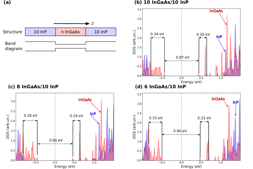
Fig. 1(b)-(d) show the computed projected DOS for (InGaAs)n/(InP)10 with . The bandgap increases as the quantum well width, characterized by , decreases due to the increasing quantum confinement. The computed bandgap is in excellent agreement with the PL experiments, as summarized in Table 2. The band alignment is about the same for all three quantum well widths: the VBO is around 0.35 eV whereas the CBO is around 0.20 eV. This falls within the range of experimental values, where the VBO and CBO were measured at 0.35 eV and 0.22 eV on average (Refs. Skolnick et al. (1986); Vurgaftman et al. (2001); Adachi et al. (2009) and references therein).
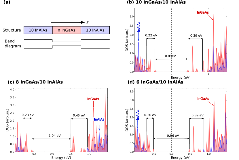
Fig. 2(b)-(d) show the computed projected DOS for (InGaAs)n/(InAlAs)10 with . The bandgap also opens up with decreasing due to the stronger quantum confinement. The band alignment is roughly the same for all three quantum well widths: the VBO is around 0.22 eV whereas the CBO is around 0.41 eV. In Refs. Peng et al. (1986); Vurgaftman et al. (2001) In0.53Ga0.47As (0.78 eV)/In0.52Al0.48As (1.44 eV, 5.85Å) is shown to have a VBO and CBO on average of 0.22 eV and 0.50 eV respectively; the VBO is about the same, whereas the CBO is 0.1 eV larger than the computed values. We note that one of the lower experimental values reported is eV López-Villegas et al. (1993) and our lower computed value is consistent with the lower fraction of In used in the computation (0.5 vs lattice-matching 0.53 in experiment) López-Villegas et al. (1993).
As InP and InAlAs have similar bandgaps and lattice constants, our calculations show that InGaAs/InP has the larger VBO and the smaller CBO, whereas InGaAs/InAlAs has the larger CBO and the smaller VBO. This trend is consistent with the experiments. Generally, the VBO/CBO values depend only weakly on the quantum well width. The bandgap, however, displays an observable dependence on quantum well width, and will be discussed in Section III.3 in terms of photoluminescent measurements.
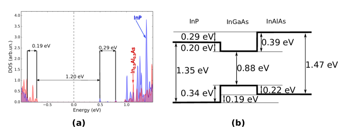
To check the transitivity of the proposed procedure, we compute the band alignment using (InAlAs)10/(InP)10, as shown in Fig. 3(a). Treating InP as the quantum well, the CBO and VBO are respectively around 0.29 eV and -0.19 eV. These values are at about the average of the experimental values Adachi et al. (2009); Vurgaftman et al. (2001). Fig. 3(b) shows the combined band diagram of all three interfaces InP/InGaAs/InAlAs. The VBOs and CBOs of these three materials are transitive within eV. This degree of non-transitivity agrees with experiment Vurgaftman et al. (2001).
III.3 Comparison to photoluminescent measurements
| Quantum well | Bandgap (theory) | PL measurement | Experimental well width |
|---|---|---|---|
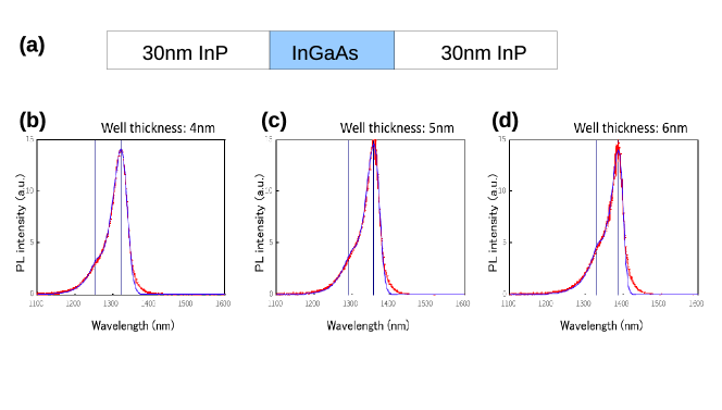
| 6InGaAs/10 InP | 0.94 eV | 0.94 eV | 4nm |
| 8 InGaAs/10 InP | 0.90 eV | 0.91 eV | 5nm |
| 10 InGaAs/10 InP | 0.87 eV | 0.89 eV | 6nm |
To further test the calculations, we prepared quantum wells of 4nm, 5nm and 6nm InGaAs as well as 30nm InP, and perform the PL measurements. The superlattice is grown using the standard MOCVD (Metal-Organic Chemical Vapour Deposition) method. The PL experiments were carried out at 300 K. The results are shown in Fig. 4. The Gaussian fits imply that the PL spectra display at least two peaks, which we interpret as the heavy hole and light hole splitting. The observed lowest-energy peak corresponds to the bandgap of the quantum well, and is summarized in Table 2. As the lattice constant is 5.86 Å, InGaAs wells of width 4nm, 5nm, 6nm are close to 6, 8, 10 InGaAs unit cells. The computed bandgaps are also given in Table 2, and good agreement is seen.
IV Conclusion
In this paper, we demonstrate that DFT calculations using DFT can be an efficient way to determine the band alignments between two alloys. The full procedure can be divided into two steps. The first step is to determine values of a bulk alloy by automatically optimizing atomic orbital-specific values of so that the experimental bandgap and the lattice constant agree with the values obtained in the simulation. The second step is to use these fitted values in a superlattice calculation (with lattice relaxation), and the valence and conduction band offsets are then determined from the projected DOS away from the interface. We apply this procedure to InGaAs/InP, InGaAs/InAlAs, and InAlAs/InP, and are able to obtain both VBOs and CBOs consistent with experiments. The degree of non-transitivity eV in the calculated band alignments is in agreement with experiment. In addition the computed quantum-well width-dependent bandgaps of InGaAs/InP are in excellent agreement with the photoluminescent measurements. The proposed method is semi-empirical, because optimization of values requires knowledge of experimental bandgaps and lattice constants. However, it provides meaningful valence and conduction band offsets between two alloys, with the interface strain taken into account. For many semiconductor alloys the experimental data are available for at least 3 compositions, that is for and in the AxB1-xC alloy. Because empirical composition-bandgap dependencies (section II.4) are quadratic, it seems plausible that the set of values can be likewise interpolated by a quadratic polynomial. The use of a compact numerical atomic orbital basis sets as implemented in SIESTA package makes this method quite lightweight, amenable to large (200+ atoms) supercell computation on a single workstation. Because lattice relaxation is taken into account, the proposed procedure can serve as a practical method to explore the band alignments between complicated alloys.
Acknowledgement
We thank Dr. Gilles Zérah and Prof. Efthimios Kaxiras for several insightful discussions. The photoluminescent measurements were performed in Amagasaki, Japan.
References
- Yang et al. (2000) G. Yang, R. J. Hwu, Z. Xu, and X. Ma, IEEE Journal of Selected Topics in Quantum Electronics 6, 577 (2000).
- Chen et al. (1988) Y. Chen, D. Radulescu, G. Wang, F. Najjar, and L. Eastman, IEEE electron device letters 9, 1 (1988).
- Baena et al. (2015) J. P. C. Baena, L. Steier, W. Tress, M. Saliba, S. Neutzner, T. Matsui, F. Giordano, T. J. Jacobsson, A. R. S. Kandada, S. M. Zakeeruddin, et al., Energy Environ. Sci. 8, 2928 (2015).
- Scanlon et al. (2013) D. O. Scanlon, C. W. Dunnill, J. Buckeridge, S. A. Shevlin, A. J. Logsdail, S. M. Woodley, C. R. A. Catlow, M. J. Powell, R. G. Palgrave, I. P. Parkin, et al., Nat. Mater. 12 (2013).
- Kuo et al. (2005) Y.-H. Kuo, Y. K. Lee, Y. Ge, S. Ren, J. E. Roth, T. I. Kamins, D. A. B. Miller, and J. S. Harris, Nature 437 (2005).
- Kohn and Sham (1965) W. Kohn and L. J. Sham, Phys. Rev. 140, A1133 (1965).
- Peressi et al. (1990) M. Peressi, S. Baroni, A. Baldereschi, and R. Resta, Phys. Rev. B 41, 12106 (1990).
- Hybertsen (1991) M. S. Hybertsen, Applied Physics Letters 58 (1991).
- Van de Walle and Martin (1987) C. G. Van de Walle and R. M. Martin, Phys. Rev. B 35, 8154 (1987).
- Lany and Zunger (2008) S. Lany and A. Zunger, Phys. Rev. B 78, 235104 (2008).
- Hedin (1965) L. Hedin, Phys. Rev. 139, A796 (1965).
- Zhu and Louie (1991) X. Zhu and S. G. Louie, Phys. Rev. B 43, 14142 (1991).
- Perdew et al. (1996a) J. P. Perdew, M. Ernzerhof, and K. Burke, J. Chem. Phys. 105 (1996a).
- Heyd and Scuseria (2004) J. Heyd and G. E. Scuseria, J. Chem. Phys. 121, 1187 (2004).
- Anisimov et al. (1991) V. I. Anisimov, J. Zaanen, and O. K. Andersen, Phys. Rev. B 44, 943 (1991).
- Dudarev et al. (1998) S. L. Dudarev, G. A. Botton, S. Y. Savrasov, C. J. Humphreys, and A. P. Sutton, Phys. Rev. B 57, 1505 (1998).
- Lany et al. (2008) S. Lany, H. Raebiger, and A. Zunger, Phys. Rev. B 77, 241201 (2008).
- Becke and Johnson (2006) A. D. Becke and E. R. Johnson, The Journal of Chemical Physics 124, 221101 (2006).
- Becke and Roussel (1989) A. D. Becke and M. R. Roussel, Phys. Rev. A: At., Mol., Opt. Phys. 39, 3761 (1989).
- Tran and Blaha (2009) F. Tran and P. Blaha, Phys. Rev. Lett. 102, 226401 (2009).
- Waroquiers et al. (2013) D. Waroquiers, A. Lherbier, A. Miglio, M. Stankovski, S. Poncé, M. J. T. Oliveira, M. Giantom assi, G.-M. Rignanese, and X. Gonze, Phys. Rev. B 87, 075121 (2013).
- Faleev et al. (2004) S. V. Faleev, M. van Schilfgaarde, and T. Kotani, Phys. Rev. Lett. 93, 126406 (2004).
- van Schilfgaarde et al. (2006) M. van Schilfgaarde, T. Kotani, and S. Faleev, Phys. Rev. Lett. 96, 226402 (2006).
- Chantis et al. (2006) A. N. Chantis, M. van Schilfgaarde, and T. Kotani, Phys. Rev. Lett. 96, 086405 (2006).
- Kang and Hybertsen (2010) W. Kang and M. S. Hybertsen, Phys. Rev. B 82, 085203 (2010).
- Wadehra et al. (2010) A. Wadehra, J. W. Nicklas, and J. W. Wilkins, Applied Physics Letters 97, 092119 (2010).
- Gmitra and Fabian (2016) M. Gmitra and J. Fabian, Phys. Rev. B 94, 165202 (2016).
- Wang et al. (2013) Y. Wang, F. Zahid, Y. Zhu, L. Liu, J. Wang, and H. Guo, Applied Physics Letters 102, 132109 (2013).
- (29) The transitivity rule refers to the following: for three semiconductors, A, B, and C, the band offset at the heterojunction A/B can be deduced from the band offsets at the heterojunctions A/C and C/B.
- Soler et al. (2002) J. M. Soler, E. Artacho, J. D. Gale, A. García, J. Junquera, P. Ordejón, and D. Sánchez-Portal, J. Phys.: Condens. Matter 14, 2745 (2002).
- García-Gil et al. (2009) S. García-Gil, A. García, N. Lorente, and P. Ordejon, Phys. Rev. B 79, 075441 (2009).
- Perdew et al. (1996b) J. P. Perdew, K. Burke, and M. Ernzerhof, Phys. Rev. Lett. 77, 3865 (1996b).
- Liechtenstein et al. (1995) A. I. Liechtenstein, V. I. Anisimov, and J. Zaanen, Phys. Rev. B 52, R5467 (1995).
- Cococcioni and De Gironcoli (2005) M. Cococcioni and S. De Gironcoli, Phys. Rev. B 71, 035105 (2005).
- Ivády et al. (2014) V. Ivády, R. Armiento, K. Szász, E. Janzén, A. Gali, and I. A. Abrikosov, Phys. Rev. B 90, 035146 (2014).
- Aryasetiawan et al. (2006) F. Aryasetiawan, K. Karlsson, O. Jepsen, and U. Schönberger, Phys. Rev. B 74, 125106 (2006).
- Agapito et al. (2015) L. A. Agapito, S. Curtarolo, and M. B. Nardelli, Phys. Rev. X 5, 011006 (2015).
- Kulik et al. (2016) H. J. Kulik, N. Seelam, B. D. Mar, and T. J. Mart nez, J. Phys. Chem. A 120, 5939 (2016).
- Sonomura et al. (1982) H. Sonomura, G. Sunatori, and T. Miyauchi, Journal of Applied Physics 53, 5336 (1982).
- Nahory et al. (1978) R. E. Nahory, M. A. Pollack, W. D. J. Jr., and R. L. Barns, Applied Physics Letters 33, 659 (1978).
- Minch et al. (1999) J. Minch, S. Park, T. Keating, and S. Chuang, IEEE Journal of Quantum Electronics 35 (1999).
- Zhang et al. (2011) Y. Zhang, Y. Ning, L. Zhang, J. Zhang, J. Zhang, Z. Wang, J. Zhang, Y. Zeng, and L. Wang, Opt. Express 19, 12569 (2011).
- Olego et al. (1982) D. Olego, T. Y. Chang, E. Silberg, E. A. Caridi, and A. Pinczuk, Applied Physics Letters 41, 476 (1982).
- Skolnick et al. (1986) M. S. Skolnick, P. R. Tapster, S. J. Bass, A. D. Pitt, N. Apsley, and S. P. Aldred, Semiconductor Science and Technology 1, 29 (1986).
- Vurgaftman et al. (2001) I. Vurgaftman, J. Meyer, and L. Ram-Mohan, Journal of applied physics 89, 5815 (2001).
- Adachi et al. (2009) S. Adachi, P. Capper, S. Kasap, and A. Willoughby, Properties of Semiconductor Alloys: Group-IV, III-V and II-VI Semiconductors, Wiley Series in Materials for Electronic & Optoelectronic Applications (Wiley, 2009), ISBN 9780470743690.
- Peng et al. (1986) C. K. Peng, A. Ketterson, H. Morko , and P. M. Solomon, Journal of Applied Physics 60, 1709 (1986).
- López-Villegas et al. (1993) J. López-Villegas, P. Roura, J. Bosch, J. Morante, A. Georgakilas, and K. Zekentes, Journal of The Electrochemical Society 140, 1492 (1993).