Channel thickness optimization for ultra thin and 2D chemically doped TFETs
Abstract
2D material based tunnel FETs are among the most promising candidates for low power electronics applications, since they offer ultimate gate control and high current drives that are achievable through small tunneling distances () during the device operation. The ideal device is characterized by a minimized . However, devices with the thinnest possible body do not necessarily provide the best performance. For example, reducing the channel thickness () increases the depletion width in the source which can be a significant part of the total . Hence, it is important to determine the optimum for each channel material individually. In this work, we study the optimum for three channel materials: WSe2, Black Phosphorus (BP), and InAs using full-band self-consistent quantum transport simulations. To identify the ideal for each material at a specific doping density, a new analytic model is proposed and benchmarked against the numerical simulations.
Index Terms:
tunnel transistors, channel thickness, quantum transport.I Introduction
The supply voltage of metal oxide semiconductor field-effect transistors (MOSFETs) has almost stopped scaling since the beginning of the millennium, since the sub-threshold swings in conventional transistors cannot be imporved beyond 60 mV/dec at room-temperature for fundamental reasons. Even today’s state-of-the-art 14nm tri-gate MOSFET does not operate below 0.6V [1]. For decades, the semiconductor industry has been researching transistors with steeper subthreshold characteristics than obtainable in conventional FETs with the goal to enbale low supply voltages to reduce power consumption [2, 3]. Unlike MOSFETs, tunneling field effect transistors (TFETs) are not bound by the 60mV/dec limit and can operate at significantly lower voltages [4, 5, 6, 7]. Such merit makes TFETs an appealing alternative option to MOSFETs for low power applications [8, 9]. However, TFETs utilize band to band tunneling (BTBT) to switch the device ON and OFF, and the BTBT process limits the ON current () accordingly.
is proportional to the BTBT transmission probability () which can be expressed in terms of both electrostatics and material properties [11] as
| (1) |
where in the simplest picture is the reduced effective mass along the transport direction (). is the band gap of the channel material and is the tunneling distance at the junction. Reducing increases and exponentially. For a more detailed discussion on equation (1) and its accuracy, please refer to Appendix I.
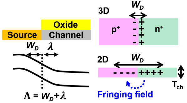
For a chemically doped TFET, the total tunneling distance () has two contributions [10, 11]: the depletion width () in the doped source region and the scaling length () in the channel as shown in Fig. 1.
Reducing the channel thickness () is beneficial in terms of electrostatics and may translate into a smaller [9] if for example does not depend on . In reality, however, is thickness dependent in a low dimensional system (i.e. 2D material). This has been demonstrated experimentally [12], numerically, and analytically [13, 12, 14, 15] where is larger in a 2D compared to a 3D PN junction. In a 2D PN junction, is inversely proportional to the thickness [13].
| (2) |
where is the doping density and is the built-in potential. is an averaged dielectric constant of the channel material and the dielectric surrounding the source. for a chemically doped double gated 2D TFET [16] can be approximated as
| (3) |
where and are the dielectric constant and the thickness of the gate oxide in Fig. 1, respectively. and are fitting parameters, since the expression without and was derived for an electrostatically doped 2D TFET [17, 16].
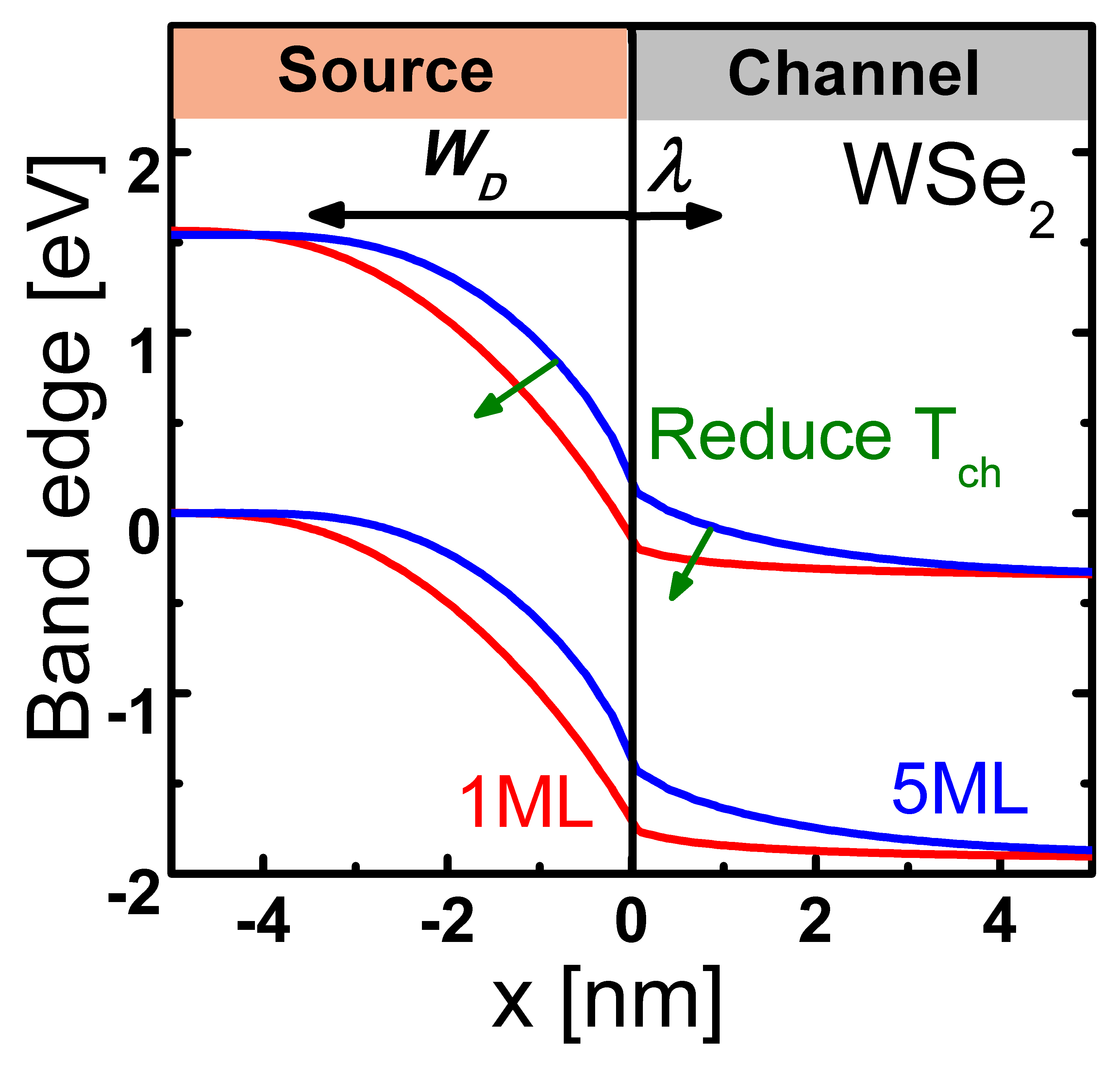
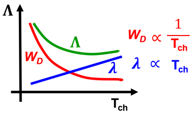
Fig. 2 shows that and respond to in the opposite fashion as illustrated in the band diagrams extracted from atomistic simulations of a mono-layer (1ML) and a 5ML WSe2 TFETs. When is reduced from 5ML to 1ML, is reduced due to the tighter gate control according to eq. (3) while increases according to eq. (2). As a result, the thinnest possible may not minimize as shown in Fig. 3.
Moreover, the channel thickness () that minimizes the total tunneling distance () is not necessarily the best overall since material parameters might change also with . To obtain the highest , the optimum should minimize the entire expression . In this work, a compact model to optimize for the ON state () is introduced, and the model is benchmarked with state-of-the-art atomistic quantum transport simulations.
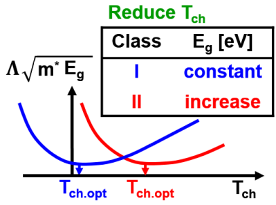
Materials considered in this article can be classified depending on how their band gap changes with . We define class I materials as those that do not show a dependence of on , which, as will be discussed below, results in thinner for optimum ON-state performance. On the other hand, class II materials, according to our definition, exhibit a decrease of with increasing . As a result, an optimum design is achieved with a relatively thicker . Details are described later.
In sections II and III, the impact of the body thickness on material properties and tunneling distance are discussed. Section IV shows the optimized for the ON-state obtained from an analytic analysis and atomistic quantum transport simulations. Section V shows the upper limit of in a TFET. Last, section VI summarizes the design rules for a TFET.
II The impact of on and
Three channel materials are considered in this work: WSe2, BP, and InAs. BP and InAs are chosen, because their small direct occurs promising for TFET applications [18, 19, 20, 21]. Note that in the case of InAs, body thicknesses beyond what has been experimentaqlly achieved were considered, and that in general transport in channels with below 5 nm is strongly impacted by surface scattering [22, 23], while our model assumes that ballistic transport conditions prevail. WSe2 is chosen as a case study, since its direct band gap () barely changes with . Moreover, WSe2 based TFETs are expected to show the best performance among semiconducting transition metal dichalcogenides (TMDs) [24, 25, 26].
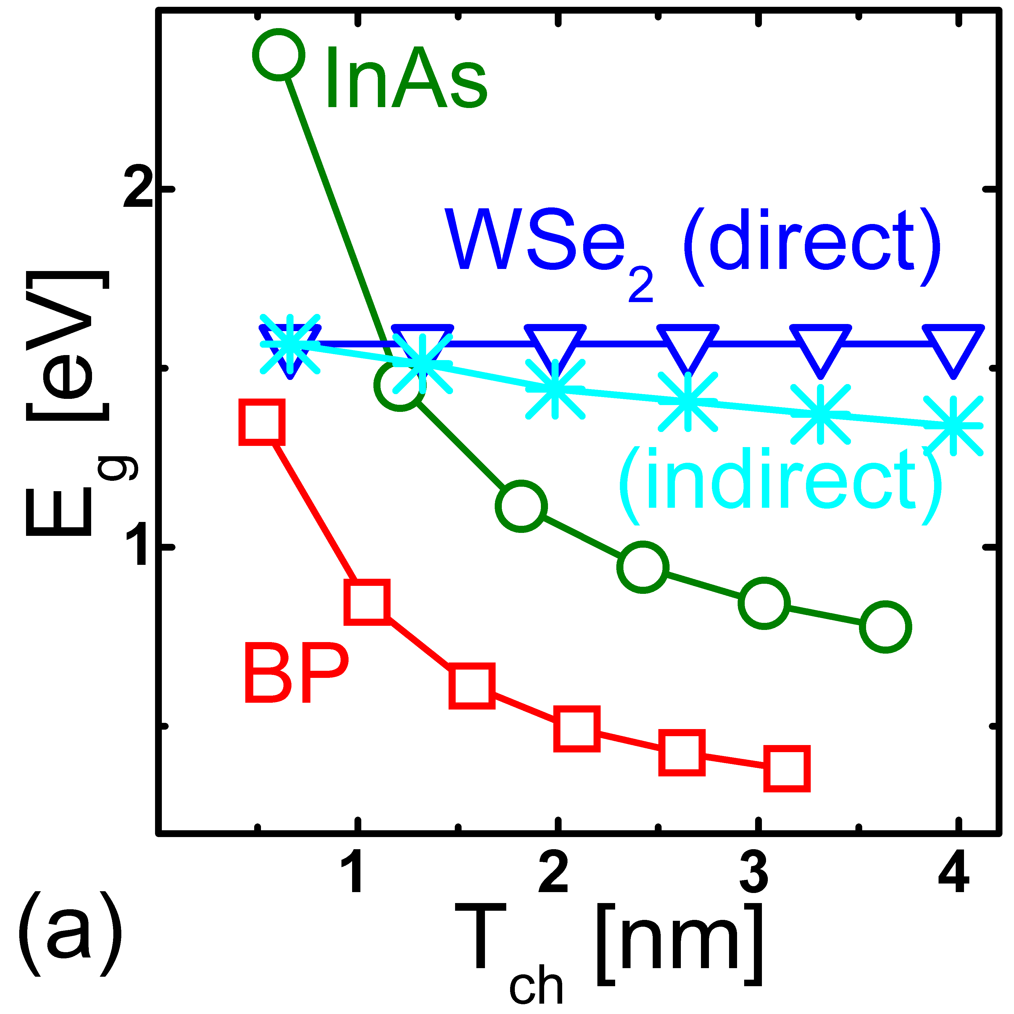
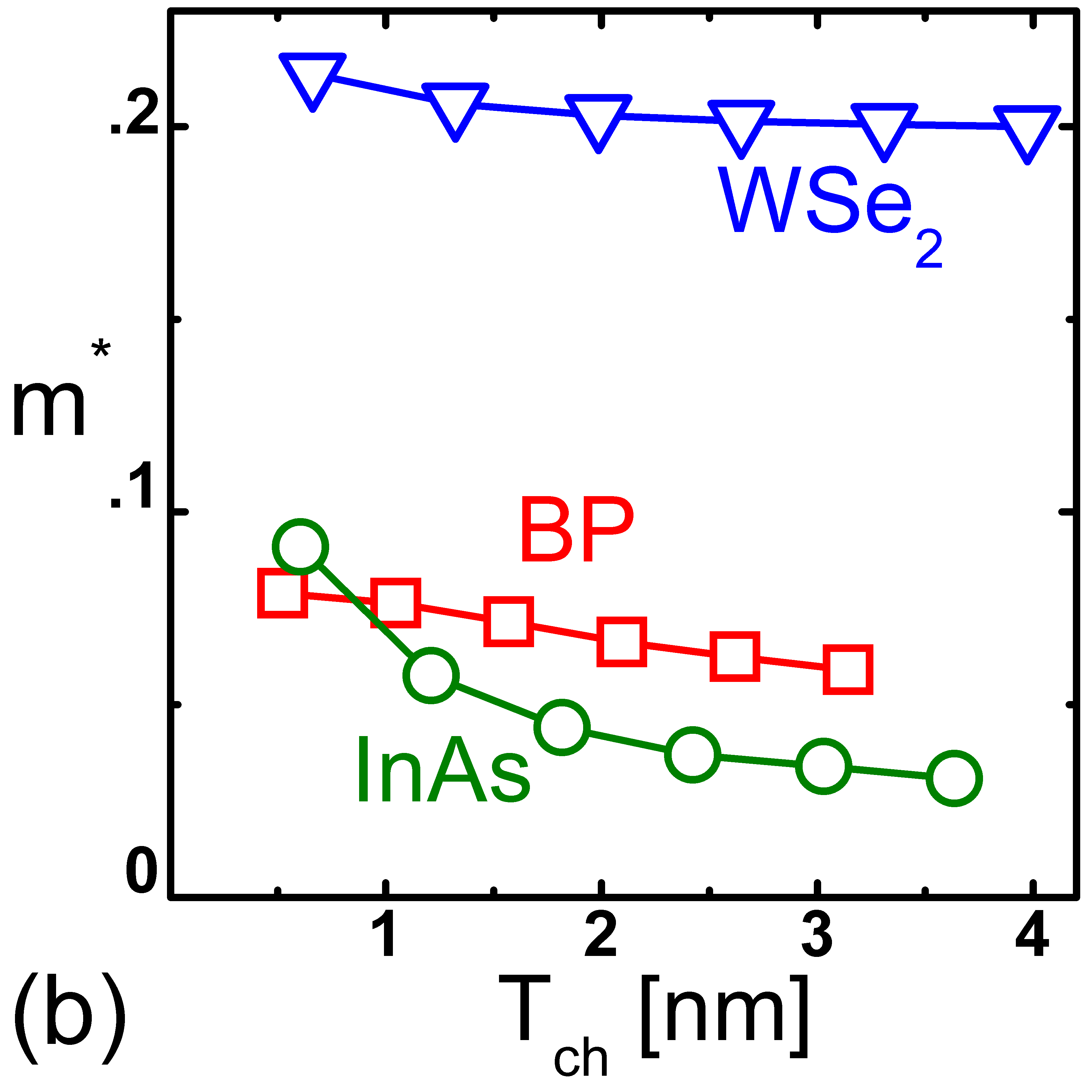
Fig. 5 shows and tunneling mass of WSe2, BP, and InAs extracted from atomistic tight binding simulations. The Slater-Koster tight binding parameters [27] of WSe2 are extracted from the band structure calculated by density function theory (DFT) with generalized gradient approximation (GGA) [24, 28]. Note that is not exactly the same as in some transport experiments [29], but is comparable.
and typically increase with stronger confinement achieved by reducing . The dependence of and on can be expressed as and . and are determined from Fig. 5 by fitting. The parameter for the case of WSe2 is significantly smaller than in the case of BP and InAs due to weak inter-layer coupling [30, 31].
channel [eV] [eV/nm] [] [] WSe2 1.535 0.02 0.2 0.01 BP 0.28 0.52 0.055 0.02 InAs 0.35 1.5 0.025 0.035
III The impact of on the tunneling distance
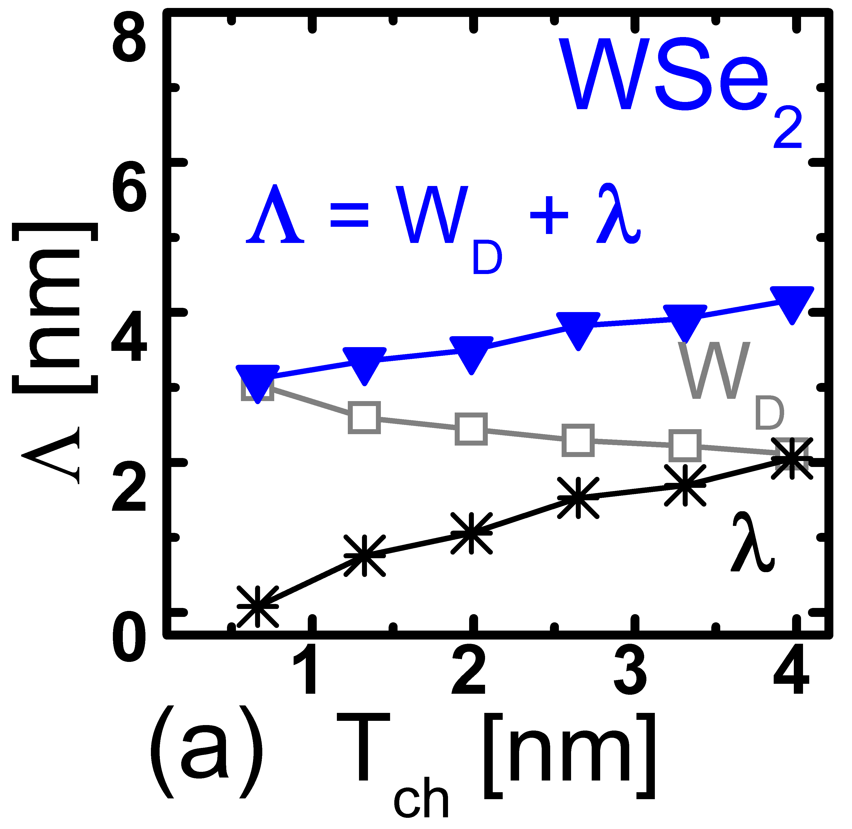
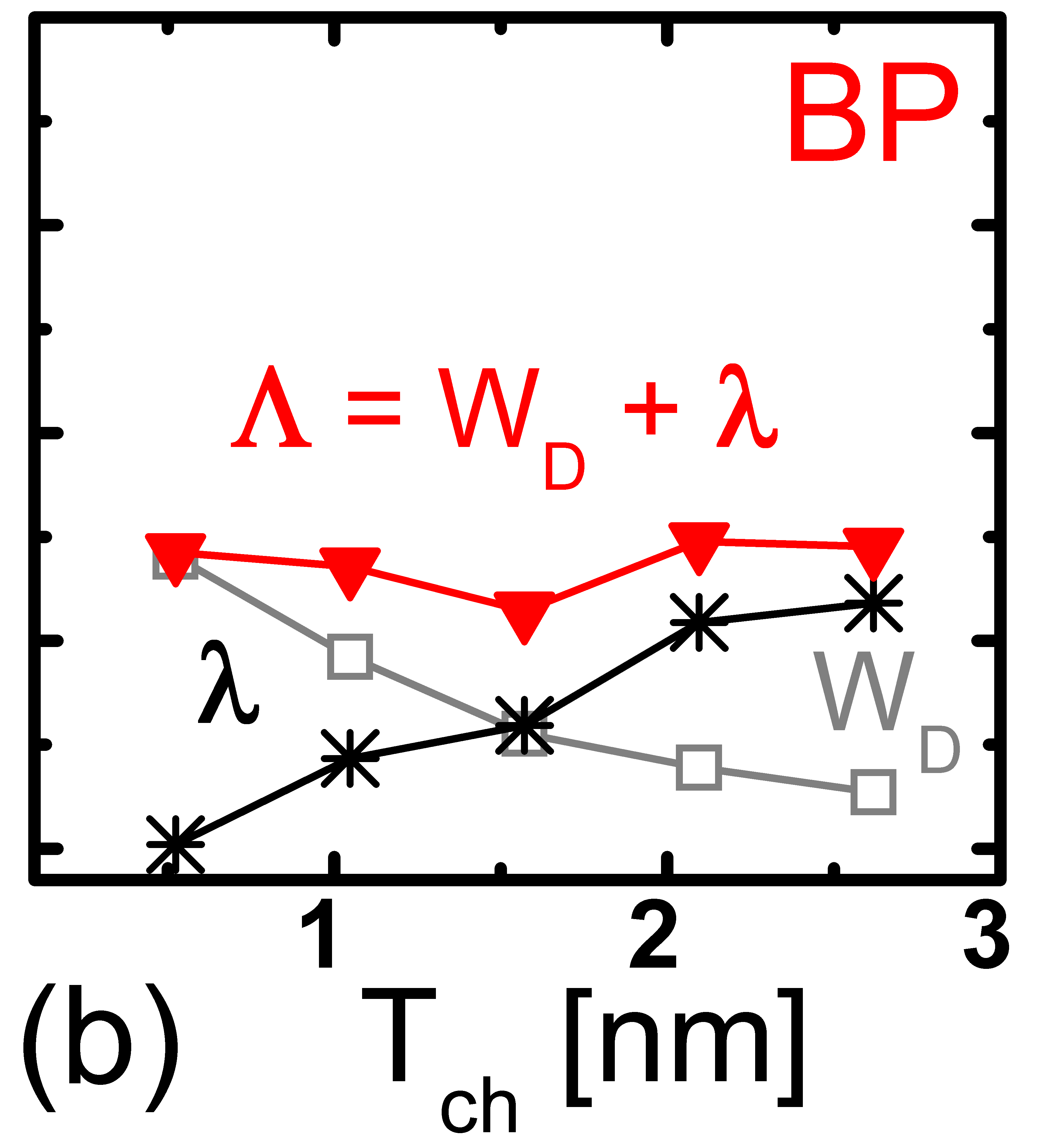
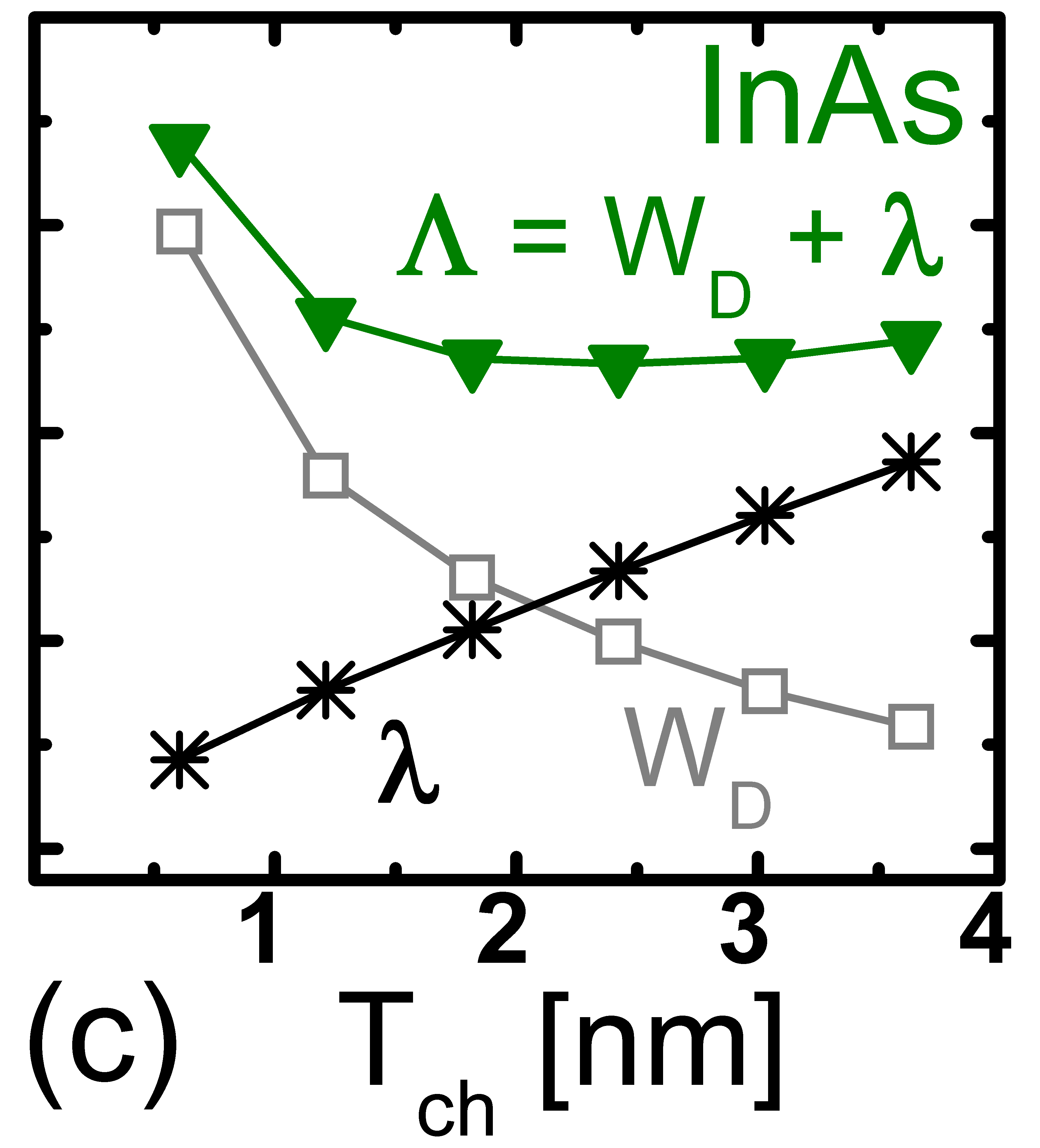
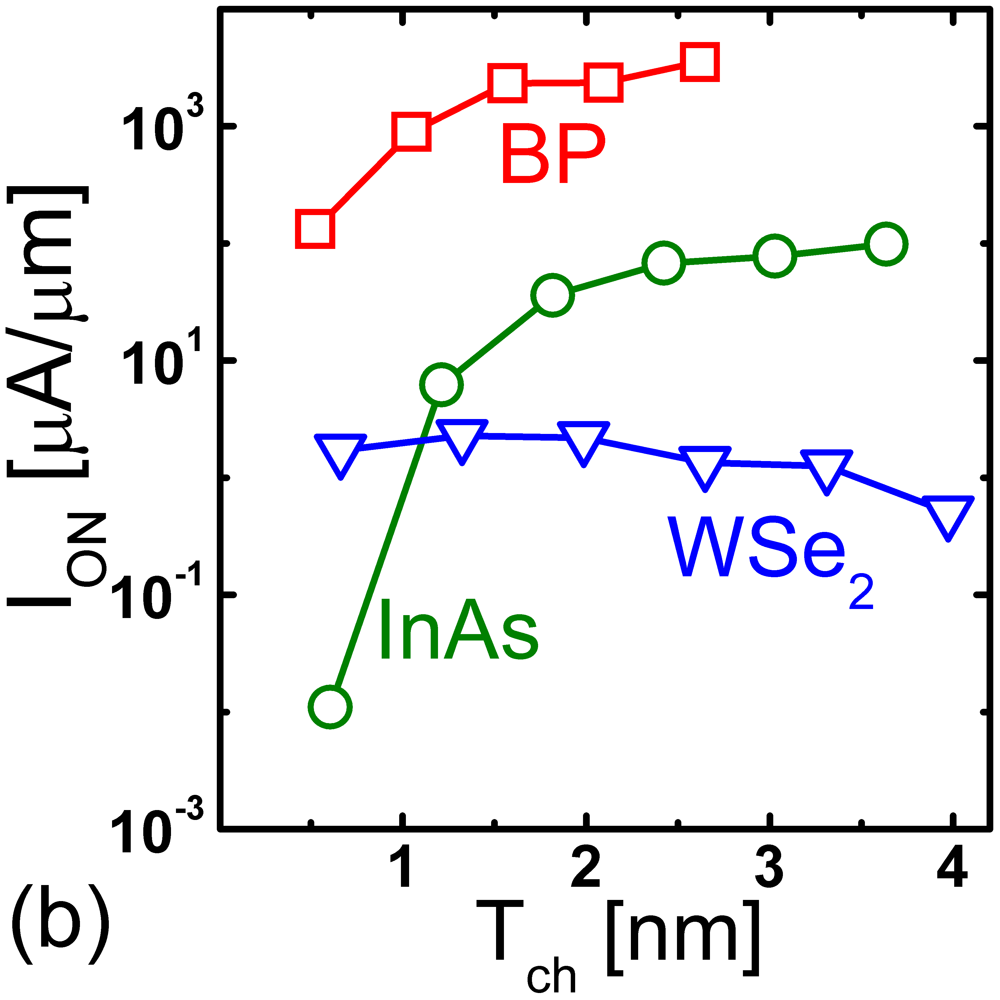
WSe2, BP, and InAs 2D TFETs’ , , and are shown in Fig. 6 (a), (b), and (c). The source doping density (N) is . All simulated materials show that is proportional to while is inversely proportional to . The data are extracted from atomistic quantum transport simulations. The details of the simulation method and the simulated structure is described in Appendix II. in the ON-state is proportional to the potential drop () across the depletion layer in the source, which is of the order of . Since of of BP and InAs has a stronger dependence on compared to WSe2, their also shows a stronger dependence on .
IV The Optimum for ON-state ()
The optimum () for the ON-state minimizes and is expected to maximize . The dependence of , , and on has been discussed in section II and III. All of them can be expressed as a function of . As a result, can also be expressed as a function of and is given by
| (4) | ||||
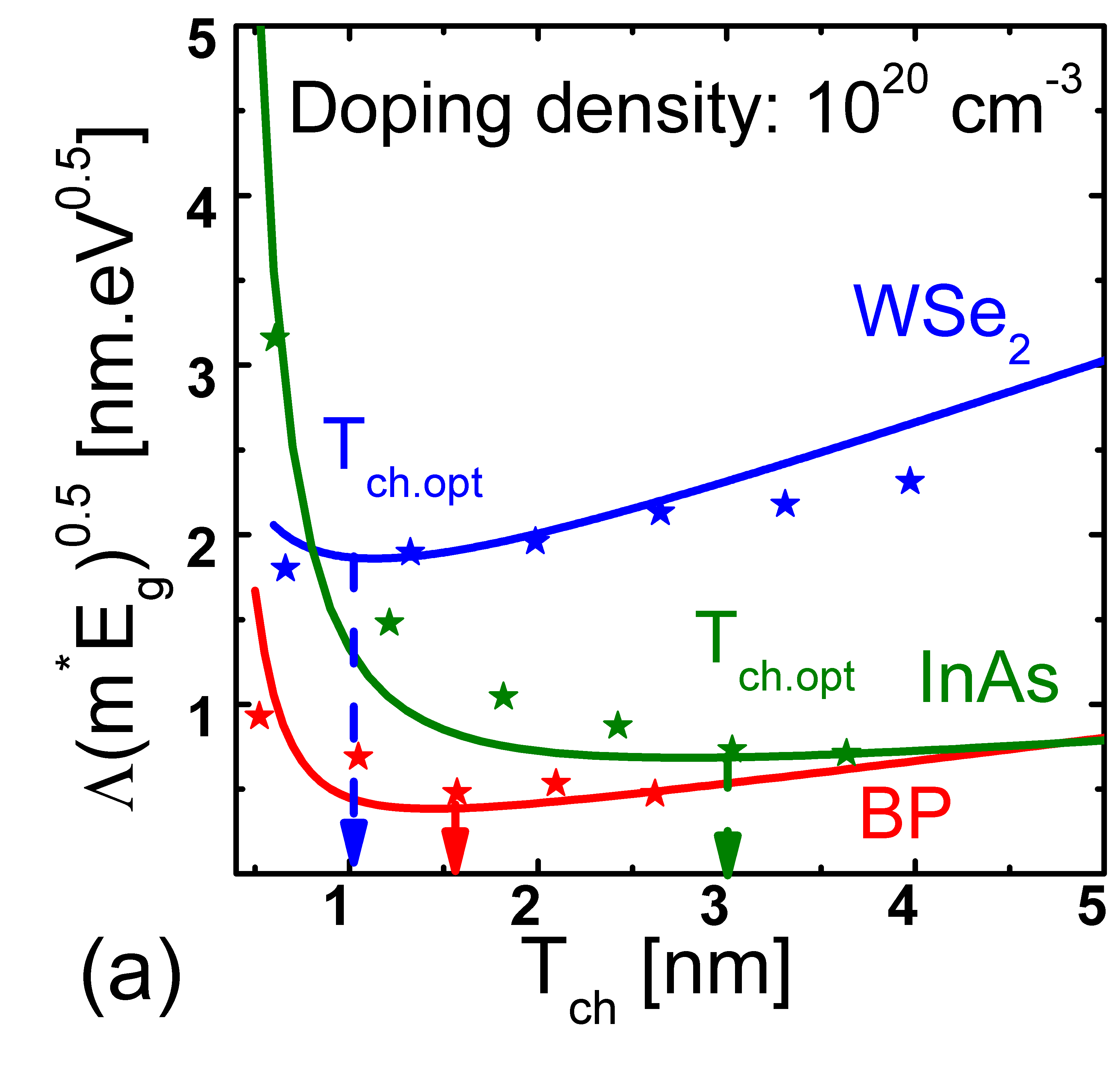
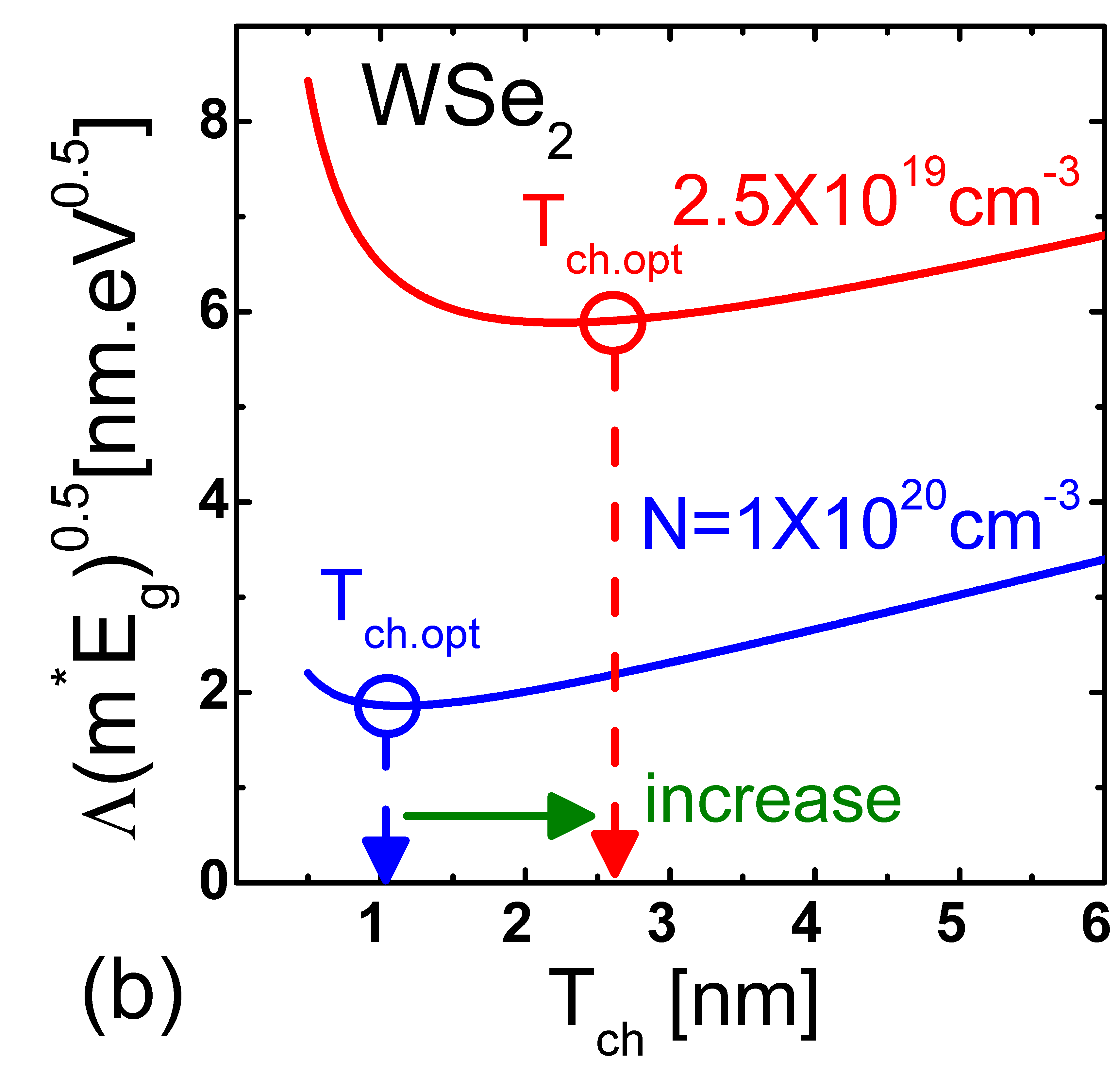
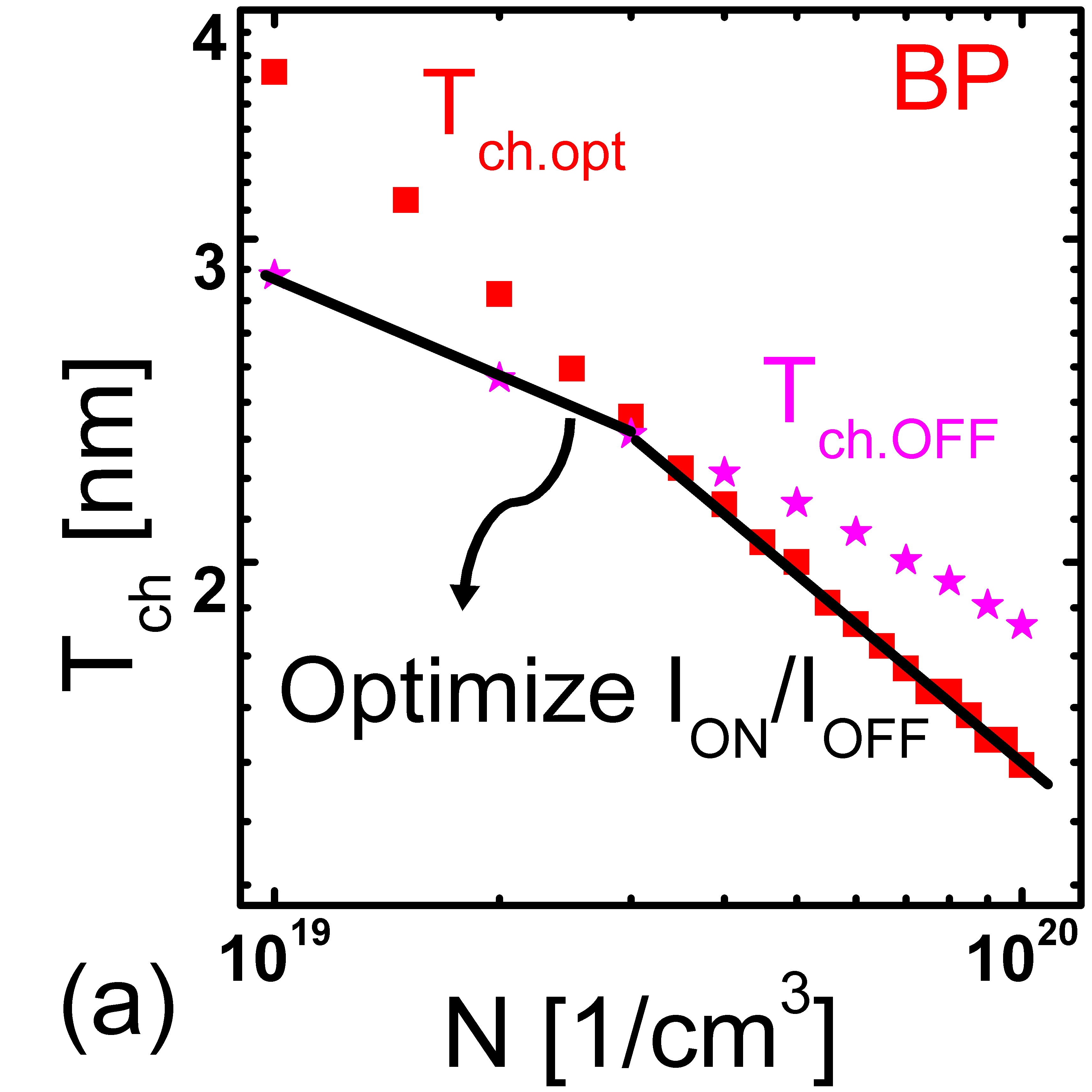
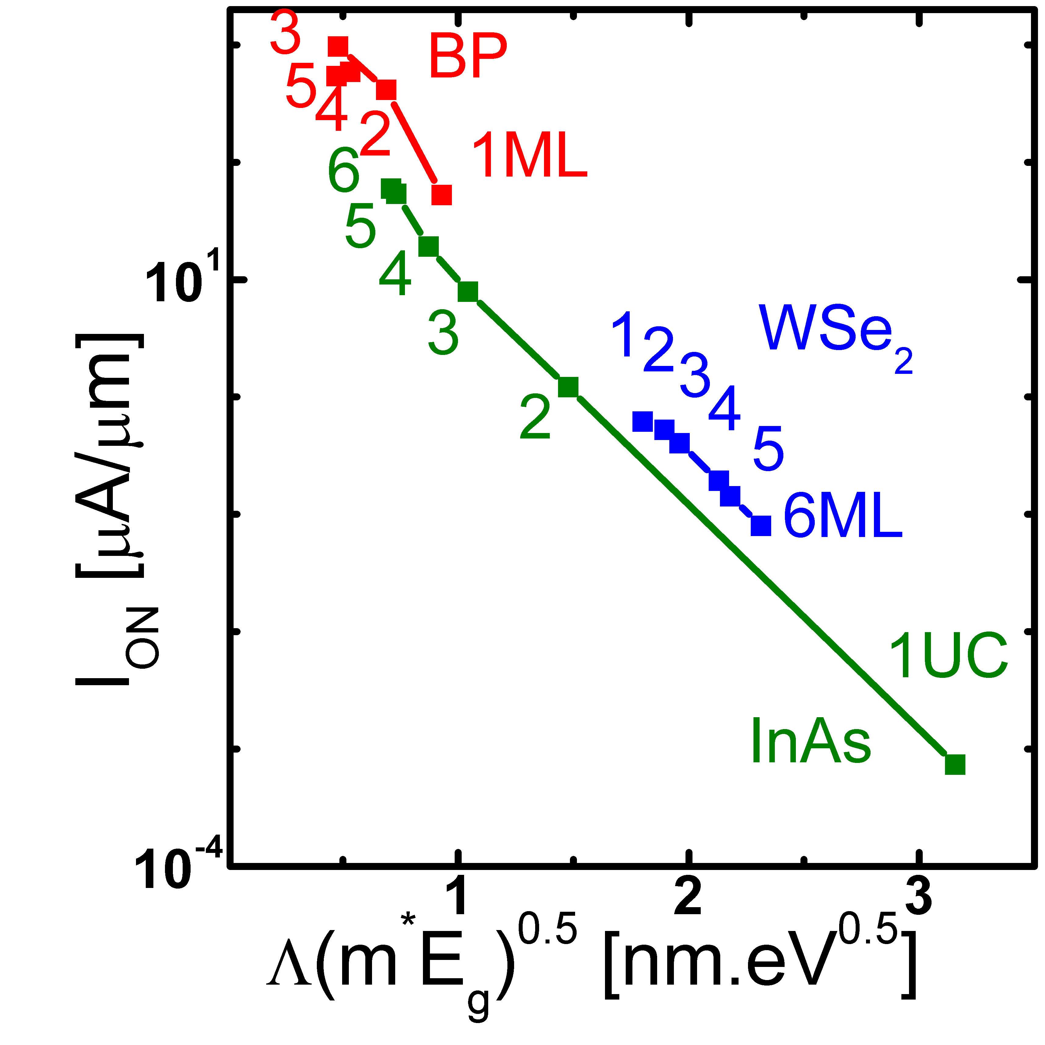
parameters are described in Appendix III in detail. Finding that minimizes can be accomplished analytically or numerically. An exact analytic solved by is complicated to interpret. Therefore, we will focus in the following on the numerical results by calculating at different and find as the minimum of those plots. Fig. 7 (a) shows for WSe2, BP, and InAs TFETs calculated form eq. (4), corresponding well with the results from atomistic quantum simulations.
It is apparent that WSe2 as a class I material exhibits a smaller as mentioned before, since 0.5 nm which is a single atomic layer’s thickness. For a class II material like BP or InAs, is larger than a mono-layer’s thickness which implies a larger . Moreover, increases when the source doping density (N) decreases as apparent from fig. 7(b), since inversely proportionally depends on N as stated above.
WSe2 BP InAs [nm] 0.01 1.8 4.3 Class I II II
V An upper limit of defined by the OFF-state ()
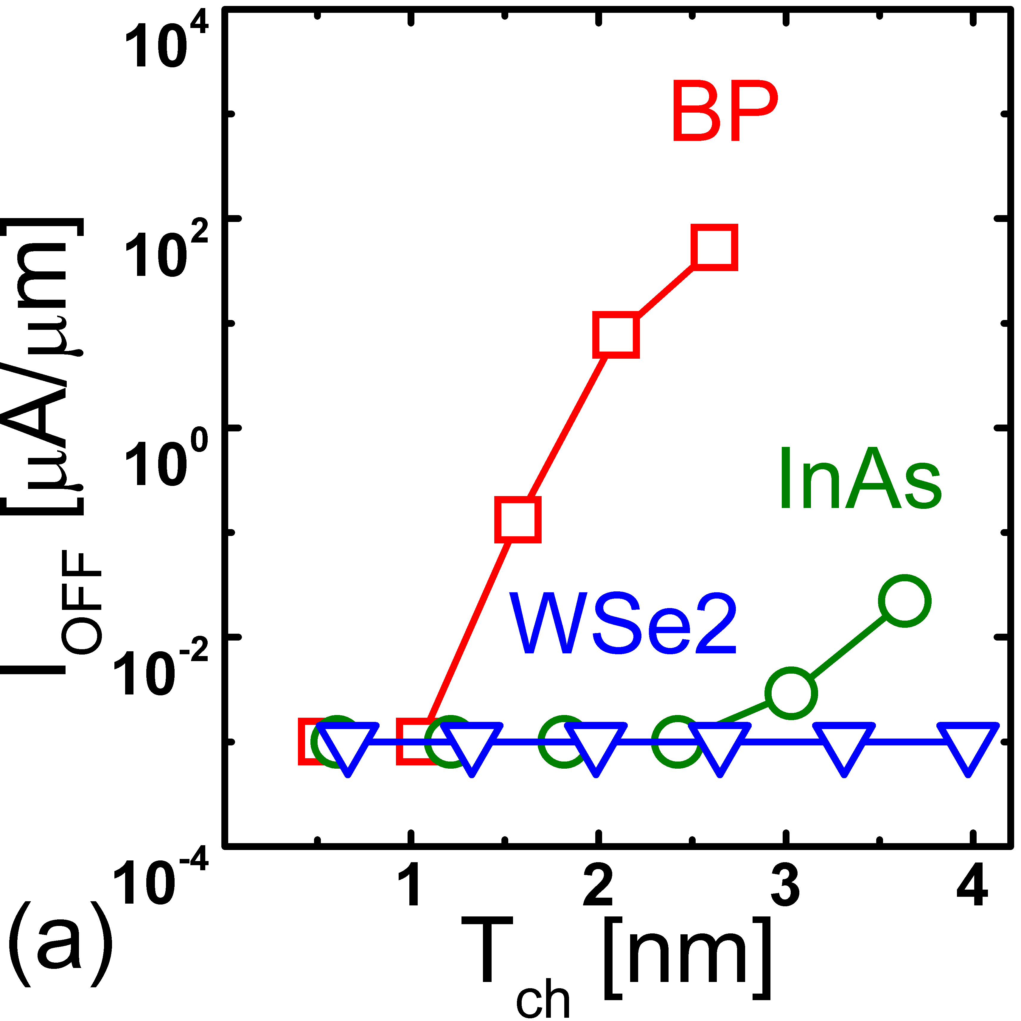
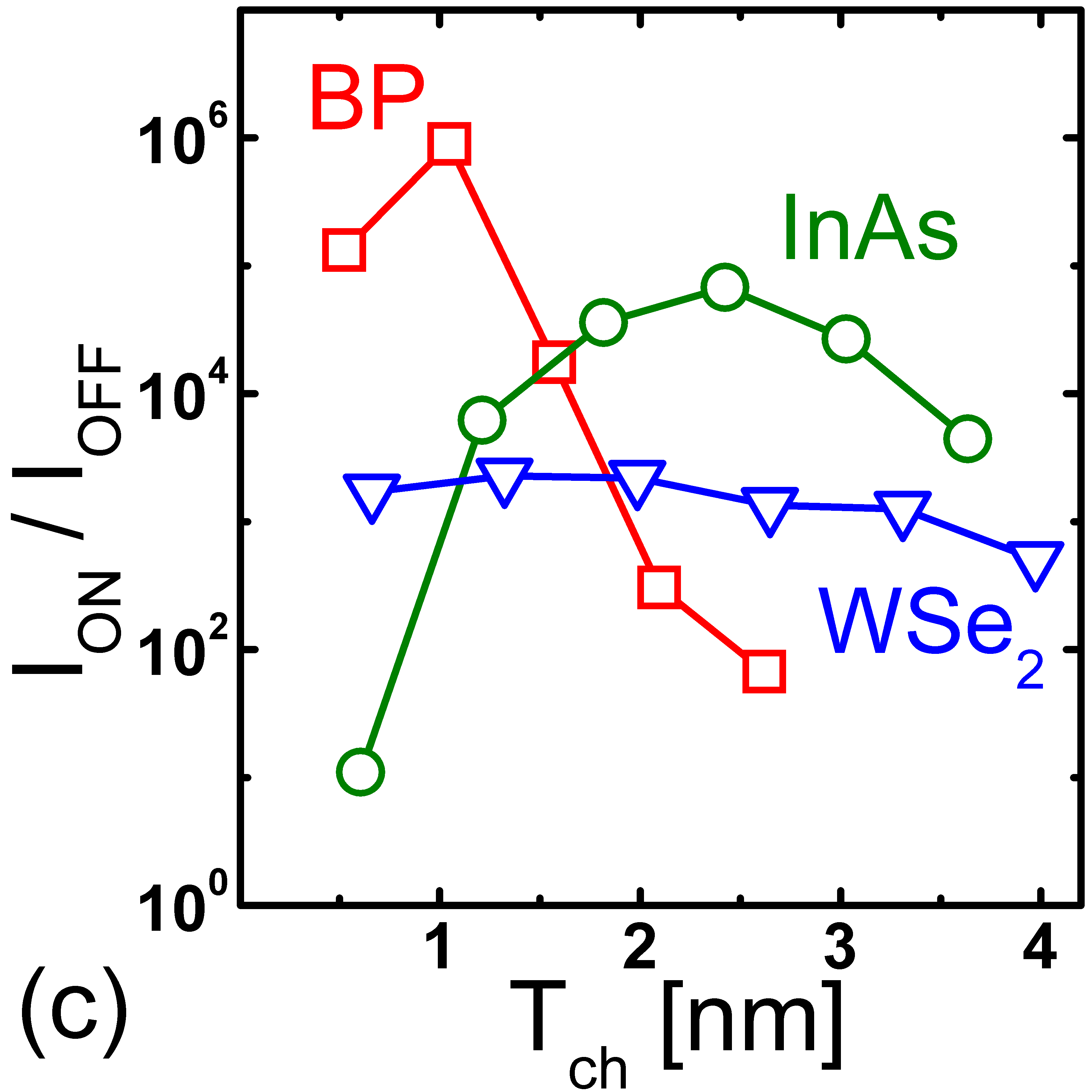
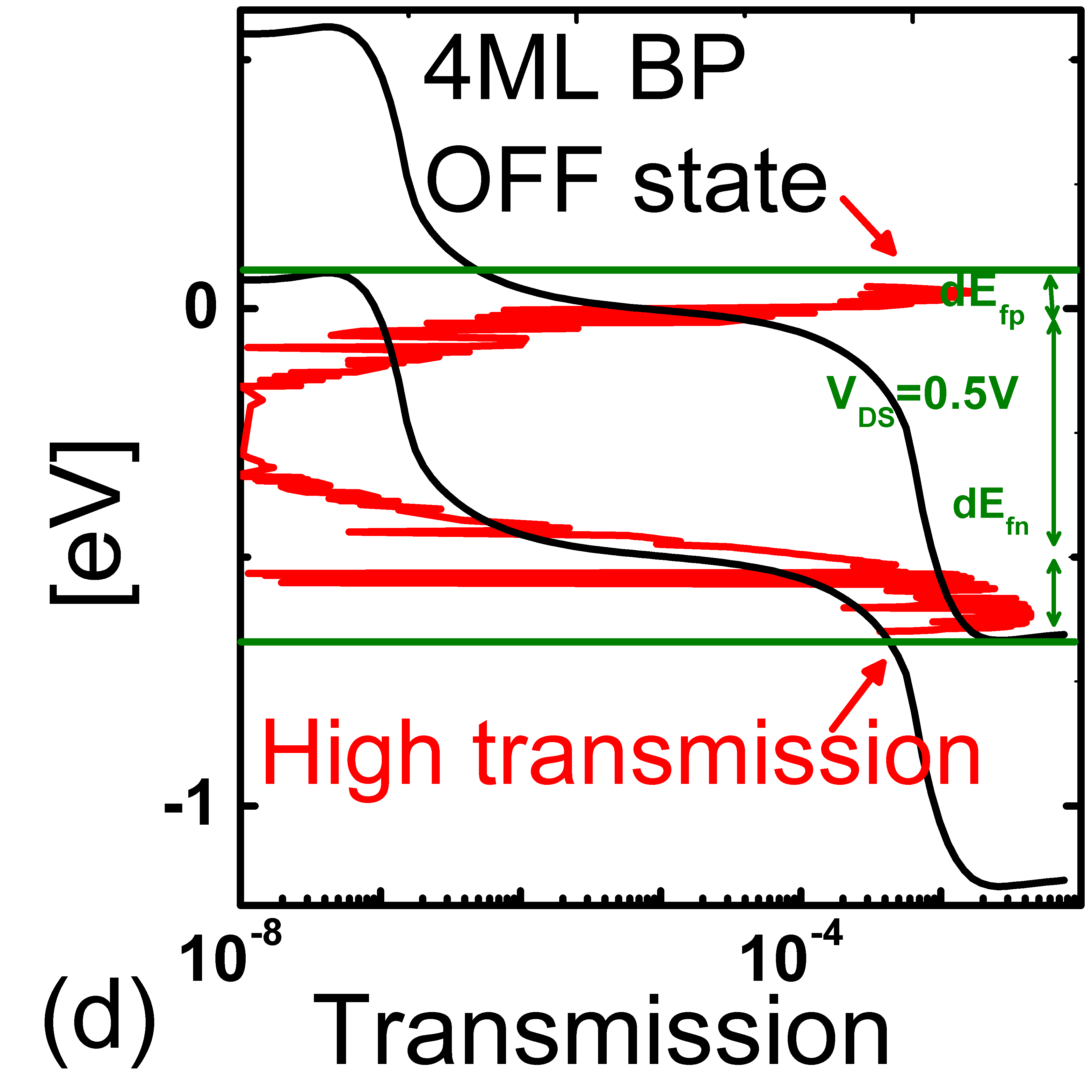
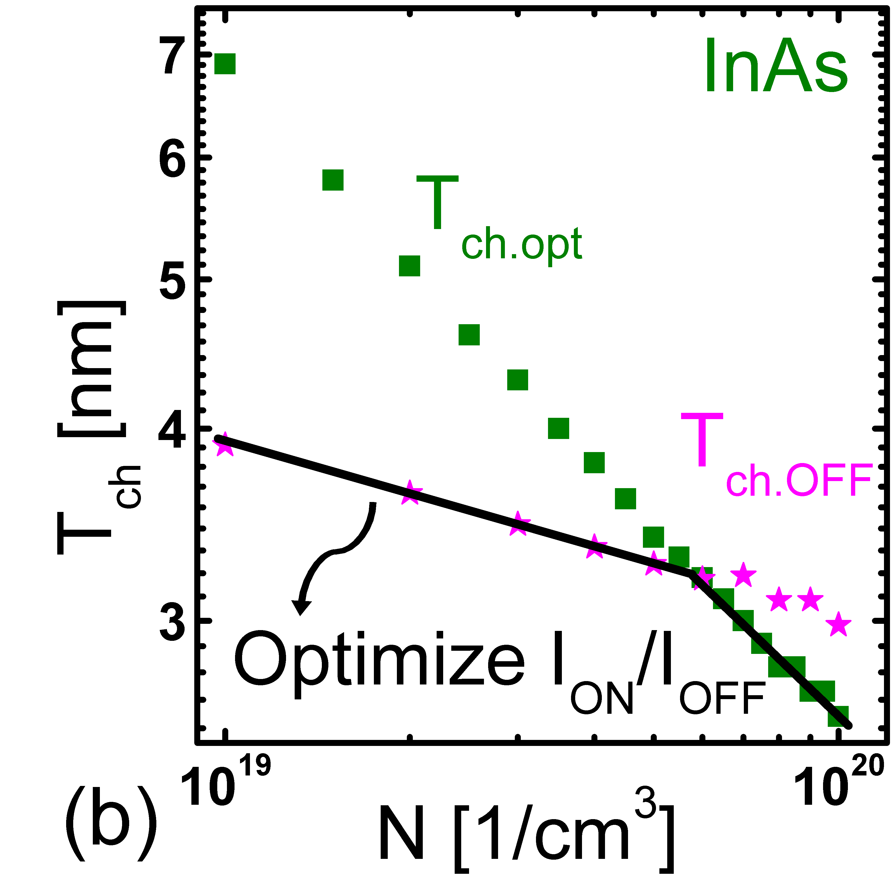
A thicker channel with a smaller bandgap may increase and deteriorate the ON/OFF current ratio. An upper limit on can be deduced by considering the maximum permissible OFF current (). Fig. 8(a), (b), and (c) show the , , and ON/OFF current ratio extracted from the curves as calculated from atomistic quantum transport simulations. The simulated structure is shown in Appendix II and assumes the supply voltage () is 0.5V. The is shifted by adjusting the OFF-state () to V. is extracted at V after shifting the curves. Following the convention of the ITRS roadmap [2], is chosen to be or the minimum possible current above this value. for BP and InAs is substantial when is above 1 nm and 3 nm respectively. This is because in this case is too small to block the tunneling current in the OFF-state as shown in the Fig. 8(d).
The ON/OFF current ratio suffers from significant degradation if the device cannot be turned off effectively as shown in Fig. 8(c). This would occur if . and are the difference between the Fermi level and the band edge in the degenerately doped source and drain region respectively. There exist a below which is large enough to suppress the OFF current. Given that, , can be expressed as
| (5) |
and reduces as the doping density decreases, which results in a larger .
To optimize a TFET’s ON/OFF current ratio, or whichever is smaller should be used. Fig. 9 (a) and (b) show how and for BP and InAs change as a function of the source doping density. Both and increase as the source doping density is reduced.
VI Summary
Optimizing the channel thickness of a 2D TFET can significantly improve its performance. The choice of the channel thickness affects both the material properties and the electrostatics. There exists a channel thickness that minimizes the tunneling distance. However, the ON-state channel thickness () should optimize the product of the band gap, reduced effective mass and square of the tunneling distance. Moreover, a maximum permissible channel thickness () is needed to reach acceptable OFF-currents. In this work, compact models were introduced to describe these two important channel thicknesses. A 2D TFET exhibits the highest ON/OFF current ratio when the channel thickness is chosen to be the smaller of and .
Appendix I. How descriptive is ?
Knowing how descriptive is compared to sophisticated quantum transport simulations is critical before optimizing by minimizing . Fig. 10 shows and its corresponding from full band self consistent atomistic simulations.
This compact equation quantitatively represents the trend of sophisticated atomistic simulations, although it assumes a simple potential distribution and a simple [11], Different materials that have the same are expected to provide within the same order of magnitude. However, we find minor deviations between different materials because this compact equation approximates complex band structures by a single band reduced effective mass and ignores contributions from higher sub-bands. To demonstrate the descriptiveness of this compact equation, and in Fig. 10 are extracted when the tunneling window is opened to 0.35 eV to reduce contributions from higher sub-bands.
Appendix II. Simulation Details
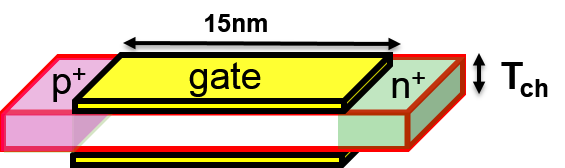
A schematic structure of the simulated double gated chemically doped TFET is shown in Fig. 11. The channel is 15 nm with the supply voltage () following the ITRS 15nm technology node [32]. The oxide is assumed to be HFO2 with an EOT of 0.5 nm. The source is heavily doped at density 1/.
The numerical simulations are performed self-consistently by coupling quantum trasmissting boundary method (QTBM) and 3D-Poisson equation [33]. 3D finite-difference method is used to calculate the carrier density (). The anisotropic dielectric constant is taken into account in the Poisson equation as shown in eq. (6) [34, 35].
| (6) |
where and are the in-plane and out-of-plane dielectric constants. The QTBM method is equivalent to the nonequalibrium Green’s function approach without scattering but is more computationally efficient [24]. The open boundary Schrdinder equation is solved in the following form:
| (7) |
where , , , and are energy, identity matrix, device Hamiltonian, and the total self-energy due to the open boundaries condition. and are the wave function in the device and the strengh of the carrier injection from contacts respectively. The Hamiltonian is constructed with the second nearest neighbor tight binding method. The simulation is performed by the Nanoelectronics Modeling tool: NEMO5. [36, 37] More simulation details can be found in [20] and [38].
Appendix III Analytical expression for
can be expressed as a function of as
| (8) | ||||
| (9) |
where through are obtained after expressing , , , and as a function of . The dependence of and on has been discussed in Section II.
for a 2D PN-junction is given by
| (10) | ||||
| (11) | ||||
| (12) |
which can be expressed as a function of explicitly. is of the order of which can be expressed as . increases with due to changes in the electrostatic environment and can be expressed as . and can be obtained by fitting shown in Fig. 6(a), (b), and (c).
channel [] [] WSe2 0.43 0.99 BP 0.62 0.91 InAs 0.83 1.28
On the other hand, the chemically doped TFET’s scaling length () is given by
| (13) | ||||
| (14) |
which is a modified version of the electrically doped TFETs’ [16, 17]. and can be obtained by fitting shown in Fig. 6 (a), (b), and (c).
channel [cons.] [nm] WSe2 0.7 0.12 BP 1.13 -0.46 InAs 0.94 0.35
After substituting , , , and , can be rearranged as
| (15) |
where to are
| (16) | ||||
| (17) | ||||
| (18) | ||||
| (19) | ||||
| (20) | ||||
| (21) | ||||
| (22) | ||||
| (23) |
to for the three channel materials are listed in the Table V.
| channel | ||||||||
|---|---|---|---|---|---|---|---|---|
| WSe2 | 0.7 | 1.78 | 0.85 | 0.01 | 0.554 | 0.01 | 1.24 | 0.54 |
| BP | 1.14 | -0.24 | 0.71 | 0.57 | 0.12 | 1.79 | 0.78 | 1.14 |
| InAs | 0.94 | 0.91 | 2.77 | 1.56 | 0.09 | 4.28 | 1.60 | 1.04 |
References
- [1] M. Bohr, “Intel s Revolutionary 22 nm Transistor Technology.” http://download.intel.com/newsroom/kits/22nm/pdfs/22nm-Details_Presentation.pdf, 2011. [Online].
- [2] “International Technology Roadmap for Semiconductors (ITRS).” http://www.itrs2.net/, 2015. [Online].
- [3] R. Gonzalez, B. Gordon, and M. Horowitz, “Supply and threshold voltage scaling for low power CMOS,” IEEE Journal of Solid-State Circuits, vol. 32, no. 8, pp. 1210–1216, 1997.
- [4] J. Appenzeller, Y.-M. Lin, J. Knoch, and P. Avouris, “Band-to-band tunneling in carbon nanotube field-effect transistors,” Phys. Rev. Lett., vol. 93, p. 196805, Nov 2004.
- [5] J. Appenzeller, Y. M. Lin, J. Knoch, Z. Chen, and P. Avouris, “Comparing carbon nanotube transistors - the ideal choice: A novel tunneling device design,” IEEE Transactions on Electron Devices, vol. 52, no. 12, pp. 2568–2576, 2005.
- [6] W. Y. Choi, B.-g. Park, J. D. Lee, and T.-j. K. Liu, “Tunneling field-effect transistors ( tfets ) with subthreshold swing ( ss ) less than 60 mv / dec,” vol. 28, no. 8, pp. 743–745, 2007.
- [7] A. M. Ionescu and H. Riel, “Tunnel field-effect transistors as energy-efficient electronic switches,” Nature, vol. 479, no. 7373, pp. 329–337, 2011.
- [8] A. C. Seabaugh and Q. Zhang, “Low-voltage tunnel transistors for beyond CMOS logic,” Proceedings of the IEEE, vol. 98, no. 12, pp. 2095–2110, 2010.
- [9] U. E. Avci, D. H. Morris, and I. a. Young, “Tunnel field-effect transistors: Prospects and challenges,” IEEE Journal of the Electron Devices Society, vol. 3, no. 3, pp. 88–95, 2015.
- [10] R. B. Salazar, H. Ilatikhameneh, R. Rahman, G. Klimeck, and J. Appenzeller, “A predictive analytic model for high-performance tunneling field-effect transistors approaching non-equilibrium Green’s function simulations,” Journal of Applied Physics, vol. 118, no. 16, 2015.
- [11] H. Ilatikhameneh, R. B. Salazar, G. Klimeck, R. Rahman, and J. Appenzeller, “From fowler-nordheim to nonequilibrium green’s function modeling of tunneling,” IEEE Transactions on Electron Devices, vol. 63, pp. 2871–2878, July 2016.
- [12] D. Reuter, C. Werner, a. D. Wieck, and S. Petrosyan, “Depletion characteristics of two-dimensional lateral p-n-junctions,” Applied Physics Letters, vol. 86, no. 16, pp. 1–3, 2005.
- [13] H. Ilatikhameneh, T. Ameen, F. Chen, H. Sahasrabudhe, G. Klimeck, and R. Rahman, “Dramatic Impact of Dimensionality on the Electrostatics of PN Junctions,” pp. 1–5, 2017.
- [14] A. Nipane, S. Jayanti, A. Borah, and J. T. Teherani, “Electrostatics of lateral p-n junctions in atomically thin materials,” Journal of Applied Physics, vol. 122, no. 19, 2017.
- [15] H. Yu, A. Kutana, and B. I. Yakobson, “Carrier Delocalization in Two-Dimensional Coplanar p-n Junctions of Graphene and Metal Dichalcogenides,” Nano Letters, vol. 16, no. 8, pp. 5032–5036, 2016.
- [16] H. Ilatikhameneh, T. a. Ameen, G. Klimeck, J. Appenzeller, and R. Rahman, “Dielectric engineered tunnel field-effect transistor,” IEEE Electron Device Letters, vol. 36, no. 10, pp. 1097–1100, 2015.
- [17] H. Ilatikhameneh, G. Klimeck, J. Appenzeller, and R. Rahman, “Scaling theory of electrically doped 2d transistors,” IEEE Electron Device Letters, vol. 36, no. 7, pp. 726–728, 2015.
- [18] H. Ilatikhameneh, T. Ameen, B. Novakovic, Y. Tan, G. Klimeck, and R. Rahman, “Saving Moore’s Law Down to 1 nm Channels with Anisotropic Effective Mass,” Scientific Reports, vol. 6, no. August, pp. 1–6, 2016.
- [19] G. B. Beneventi, E. Gnani, A. Gnudi, S. Reggiani, and G. Baccarani, “Dual-metal-gate InAs tunnel FET with enhanced turn-on steepness and high on-current,” IEEE Transactions on Electron Devices, vol. 61, no. 3, pp. 776–784, 2014.
- [20] T. A. Ameen, H. Ilatikhameneh, G. Klimeck, and R. Rahman, “Few-layer phosphorene: An ideal 2d material for tunnel transistors,” Scientific Reports, vol. 6, pp. 28515 EP –, Jun 2016. Article.
- [21] A. C. Ford, C. W. Yeung, S. Chuang, H. S. Kim, E. Plis, S. Krishna, C. Hu, and A. Javey, “Ultrathin body InAs tunneling field-effect transistors on Si substrates,” Applied Physics Letters, vol. 98, no. 11, pp. 98–100, 2011.
- [22] K. Tomioka, M. Yoshimura, and T. Fukui, “Steep-slope tunnel field-effect transistors using III-V nanowire/Si heterojunction,” Digest of Technical Papers - Symposium on VLSI Technology, no. 2010, pp. 47–48, 2012.
- [23] D. Cutaia, K. E. Moselund, H. Schmid, M. Borg, a. Olziersky, and H. Riel, “Complementary III-V heterojunction lateral NW Tunnel FET technology on Si,” Digest of Technical Papers - Symposium on VLSI Technology, vol. 2016-Septe, no. 619509, pp. 4–5, 2016.
- [24] H. Ilatikhameneh, “Tunnel field-effect transistors in 2-D transition metal dichalcogenide materials,” Ieee J. Explor. Solid State Computat. Devices Circuits, vol. 1, no. April, pp. 12–18, 2015.
- [25] H. Ilatikhameneh, G. Klimeck, J. Appenzeller, and R. Rahman, “Design rules for high performance tunnel transistors from 2-D materials,” IEEE Journal of the Electron Devices Society, vol. 4, no. 5, pp. 260–265, 2016.
- [26] Y. Ma, B. Liu, A. Zhang, L. Chen, M. Fathi, C. Shen, A. N. Abbas, M. Ge, M. Mecklenburg, and C. Zhou, “Reversible Semiconducting-to-Metallic Phase Transition in Chemical Vapor Deposition Grown Monolayer and Applications for Devices,” ACS Nano, vol. 9, no. 7, pp. 7383–7391, 2015.
- [27] J. C. S. Koster and G. F., “Simplified LCAO Methos for periodic potential problem,” vol. 94, 1954.
- [28] C. Gong, H. Zhang, W. Wang, L. Colombo, R. M. Wallace, and K. Cho, “Band alignment of two-dimensional transition metal dichalcogenides: Application in tunnel field effect transistors,” Applied Physics Letters, vol. 103, no. 5, 2013.
- [29] A. Prakash, H. Ilatikhameneh, P. Wu, and J. Appenzeller, “Understanding contact gating in Schottky barrier transistors from 2D channels,” Scientific Reports, vol. 7, no. 1, pp. 1–30, 2017.
- [30] K. Novoselov, a. Mishchenko, a. Carvalho, and a. H. Castro Neto, “2d materials and van der waals heterostructures,” Science, vol. 353, no. 6298, pp. 1–25, 2016.
- [31] K. C. Wang, T. K. Stanev, D. Valencia, J. Charles, A. Henning, V. K. Sangwan, A. Lahiri, D. Mejia, P. Sarangapani, M. Povolotskyi, A. Afzalian, J. Maassen, G. Klimeck, M. C. Hersam, L. J. Lauhon, N. P. Stern, and T. Kubis, “Control of interlayer physics in 2H transition metal dichalcogenides,” Journal of Applied Physics, vol. 122, no. 22, 2017.
- [32] B. Hoefflinger, “Itrs 2028—international roadmap of semiconductors.”
- [33] M. Luisier, A. Schenk, W. Fichtner, and G. Klimeck, “Atomistic simulation of nanowires in the tight-binding formalism: From boundary conditions to strain calculations,” Phys. Rev. B, vol. 74, p. 205323, Nov 2006.
- [34] V. Wang, Y. Kawazoe, and W. T. Geng, “Native point defects in few-layer phosphorene,” Physical Review B - Condensed Matter and Materials Physics, vol. 91, no. 4, pp. 1–9, 2015.
- [35] A. Kumar and P. K. Ahluwalia, “Tunable dielectric response of transition metals dichalcogenides MX 2 (M=Mo, W; X=S, Se, Te): Effect of quantum confinement,” Physica B: Condensed Matter, vol. 407, no. 24, pp. 4627–4634, 2012.
- [36] S. Steiger, M. Povolotskyi, H. H. Park, T. Kubis, and G. Klimeck, “NEMO5: A parallel multiscale nanoelectronics modeling tool,” IEEE Transactions on Nanotechnology, vol. 10, no. 6, pp. 1464–1474, 2011.
- [37] J. E. Fonseca, T. Kubis, M. Povolotskyi, B. Novakovic, a. Ajoy, G. Hegde, H. Ilatikhameneh, Z. Jiang, P. Sengupta, Y. Tan, and G. Klimeck, “Efficient and realistic device modeling from atomic detail to the nanoscale,” Journal of Computational Electronics, vol. 12, no. 4, pp. 592–600, 2013.
- [38] H. Ilatikhameneh, T. A. Ameen, C. Chen, G. Klimeck, and R. Rahman, “Sensitivity challenge of steep transistors,” IEEE Transactions on Electron Devices, vol. 65, pp. 1633–1639, April 2018.