Direct-gap materials hold promises for excitonic insulator. In contrast to indirect-gap materials, here the difficulty to distinguish from a Peierls charge density wave is circumvented. However, direct-gap materials still suffer from the divergence of polarizability when the band gap approaches zero, leading to diminishing exciton binding energy. We propose that one can decouple the exciton binding energy from the band gap in materials where band-edge states have the same parity. First-principles calculations of two-dimensional GaAs and experimentally mechanically exfoliated single-layer TiS3 lend solid supports to the new principle.
Realizing intrinsic excitonic insulator by decoupling exciton binding energy from the minimum band gap
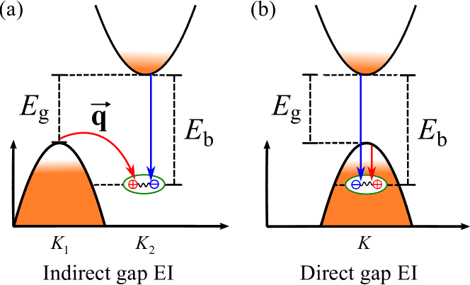
Excitonic insulator (EI) is a new state of matter with a many-body ground state. It was named in 1967Kohn , where the exciton binding energy () exceeds the bandgap (), leading to the renormalization of the single-electron band structure in a semiconductor or a semimetal against the spontaneous formation of excitons. Because the exciton is made of two fermions, it obeys the bosonic statistics on the scale larger than the exciton radius, therefore allowing for a Bose condensation. As a naturally-formed electron-hole condensate, EI behaves as a perfect insulator for both charge and heat transportRontani , despite that both electrons and holes are ideal carriers for them. Hence, EI represents a highly promising and uncharted frontier in condensed matter physics, especially in the vicinity of a transition between the EI and non-EI phases. The search for EI has lasted a half century but compelling experimental evidence is still lackingKogar . Although some evidence has been provided very recently in the quantum-well systemDu , an ideal EI would be to identify the material with naturally. The few materials proposed as possible candidates include 1T-TiSe2Cercellier ; Cazzaniga ; Kogar , Ta2NiSe5Mor ; Lu ; Wakisaka , TmSe0.45Te0.55Bucher ; Bronold , iron pnictides superconductorBrydon , CaB6Zhitomirsky ; Bascones , and carbon nanotubeVarsano . In the early days, much attention was paid to materials with interacting electron-hole pockets located at different regions in the Brillouin zone for semiconductors with a small band gap or semimetals with a small band overlap to minimize the effect of screening Sherrington . Unfortunately, however, as schematically illustrated in Fig. 1(a), perceived formation of indirect excitons is always accompanied by a strong structural distortion such as a charge density wave due to the finite momentum transfer q, which makes it difficult to determine whether the observed instability is originated from an excitonic effect or a band-type Jahn-Teller distortionKogar ; Rossnagel . For this reason, recent interests both in theoryKaneko and experimentMor ; Lu have shifted to direct gap semiconductors such as Ta2NiSe5 where structural distortion can be quenched, in spite of its generally larger screening due to band edge transitions, as shown in Fig. 1(b).
To realize an intrinsic EI, one can engineer the band structure, e.g., through an external field modulation, to increase and/or decrease such that in an otherwise trivial semiconductor or semimetal. Intuitively, it seems trivial since external means can always yield , and then is straightforward. However, this is not the case because the and are closely correlated and generally leads to diminishing . The reason is that the is determined by the system screening which is characterized by the polarizability . Within the random phase approximation and not considering the local field effects, the polarizability may be expressedusPRL ; ZRLiu as
| (1) |
where and refer to the periodical parts of conduction and valence band Bloch states, respectively, and k is integrated over the first Brillouin zone. is a dimension-related coefficient. On the appearance, Eq. (1) exhibits an inverse relationship between and , as by definition is the smallest in a direct gap material, whereby contributing the most to . More importantly, Eq. (1) reveals that when approaches zero, is going to diverge, leading to a negligible .
So it becomes clear that, the two seemingly intimately-related physical quantities and have to be decoupled in order to alter them individually via external means. According to Eq. (1), this requires = 0, corresponding to band-edge transitions so that can be finite when . In this way, the could have no response to the reduction of , therefore allowing for via band engineering. Note that prevalently used quantum-well structures to investigate the exciton condensate are also within such a notion but utilizing the spatial separation of electron and hole to suppress the band-edge transitions. To this end, two-dimensional (2D) materials provide us a new opportunity for realizing the intrinsic EI, not only because of the orders-of-magnitude enhanced usPRL , but also because the electronic properties can be more effectively controlled by applying an electric field or a strainFiori . This can be contrasted to three-dimensional materials for which tuning and/or over a wide range still represents a formidable task.
In this work, we makes use of an intrinsic way to suppress band-edge transitions, namely, the parity, unlike the spatial separation in the quantum-well structures. That is, when the band-edge states have the same parity, transitions between them are dipole forbiddenNie so becomes very close to zero. As a result, the strongly related behaviorusPRL between and no longer holds, because the two are now derived from different states with different characteristic energies. In particular, is controlled, as usual, by the band-edge states, but is now controlled to a much lesser degree by such band-edge states but to a much larger degree by states away from the band edges. Consequently, the divergence of 2D polarizability as is prevented. In the following, we will first take the recently-proposed 2D GaAsLucking as a concrete example to illustrate how the principle come into play to result in the stabilization of the EI phase over the non-EI phase. Then we turn to the case of the mechanically exfoliated single-layer TiS3 which would transit to an EI under a compressive strain about 3%.
The density functional theory calculations were performed within the Perdew-Burke-Ernzerhof (PBE)PBE exchange correlation functional as implemented in the VASPvasp code. The plane-wave basis cutoff energy was set to 600 eV. An 18 Å vacuum layer was used to avoid spurious interactions between adjacent layers. An -centered grid was used to sample the Brillouin zone. The atomic structures were fully relaxed until residual forces on each atom were less than 0.001 eV/Å and the system dynamical stability was further confirmed by phonon calculations. Owing to the well-known band-gap underestimation by PBE, we also performed Heyd-Scuseria-Ernzerhof (HSE) hybrid functionalHSE03 ; HSE06 and many-body GWGWKress calculations, and the results are given for comparison. We used Yamboyambo code to calculate by solving the Bethe-Salpeter equation (BSE)BSELouie with the single-electron band structure produced by Quantum Espresso packagepwscf .
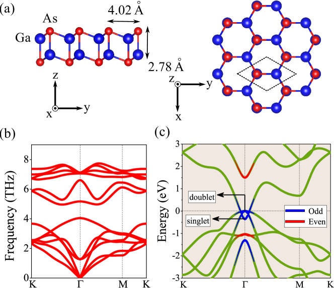
Recently, a 2D form of traditional semiconductors has been synthesized via a migration-enhanced encapsulated growth technique utilizing epitaxial grapheneBalushi . In the meantime, based on the first-principles calculations, it was predicted that the ultra-thin limit of traditional binary III-V, II-VI, and I-VII semiconductors could take the kinetically stable and energetically favorable double-layer honeycomb (DLHC) structureLucking . Intriguingly, the DLHCs have the desired properties that band-edge states have the same symmetry. Figure 2(a) shows the DLHC structure for 2D GaAs. It is made of two monolayers of buckled honeycombs vertically coupled to each other with an AB stacking. Figure 2(b) shows the calculated phonon spectrum confirming its kinetic stability. In Ref. Lucking, , ab initio molecular dynamics were also carried out to confirm the stability.
Figure 2(c) shows the PBE band structure for the GaAs. Near the Fermi energy, there are three bands, a singlet and the doubly degenerate bands (doublet) at point, which deserve special attention. Noticeably, these band edge states do have the same parity as required. However, 2D GaAs exhibits a metallic behavior instead of the usual semiconducting behavior and the doublet is above the singlet, which leads to a negative of 0.34 eV at . While having the correct parities near the Fermi level, the metallic behavior is indicative of a strong screening, which usually diminishes .
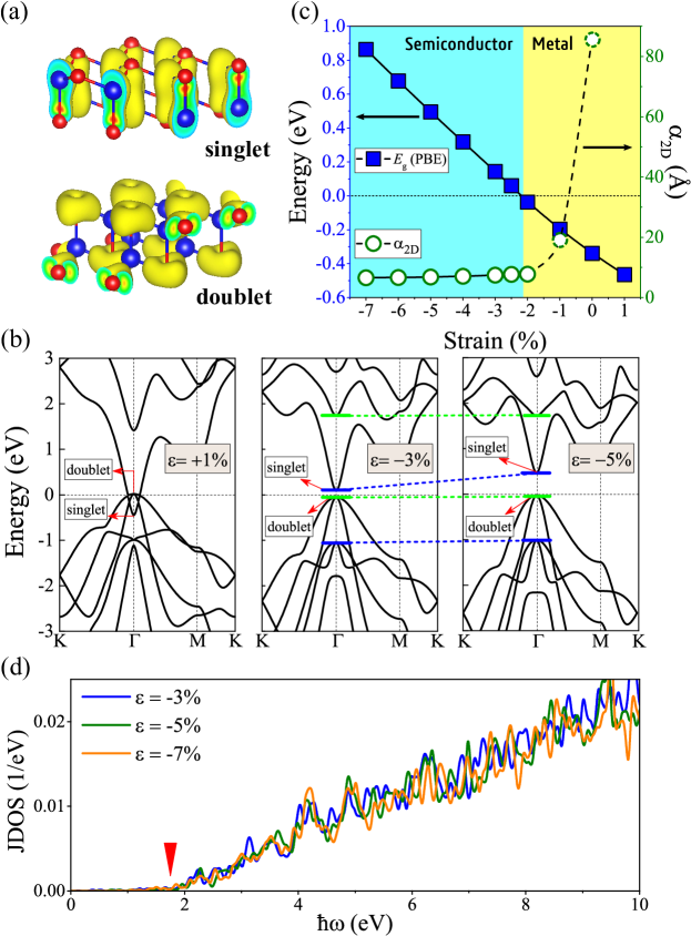
To this end, we note that strain can induce metal-semiconductor transition in 2D materialsFiori ; my2D . Moreover, we find that the charge densities of the singlet and doublet at point have different out-of-plane and in-plane characters, as can be seen in Fig. 3(a). As a result, they must have substantially different responses to applied strain. Figure 3(b) plots selectively the band structures for 2D GaAs as a function of an in-plane biaxial strain. It can be seen that when the system is compressed by 3%, band “inversion” at point is lifted to open a gap of 0.14 eV. It increases notably with the strain to 0.49 eV at 5% compression. In contrast, the 2D GaAs remains to be metallic under a tensile stain.
In Fig. 3(c), we plot the respective dependence of and 2D polarizability [derived from Eq. (1) with coefficient ] on the in-plane biaxial strain. Clearly, they behave in completely different manners. While the reveals a simple linear dependence on the strain, the keeps almost unchanged for positive and rapidly diverges when the system becomes metallic. This strongly implies the quite different responses of and to strain, hence their decoupling, as will be quantitatively demonstrated later.
We further plot the joint density of states (JDOS) under the typical strains in Fig. 3(d) in order to understand the nearly strain independent behavior of . The JDOS is calculated as
| (2) |
where is the surface area of unit cell and the measures the excitation energy. Such a quantity characterizes the number of transitions between a certain energy range . It is seen that the JDOS keeps negligible until an about 1.8 eV [Red arrow in Fig. 3(d)] and its distribution is almost invariant to the strain during the whole energy region, corresponding to the strain independence of as shown in Fig. 3(c). In addition, the existence of such a critical energy seems as if it was a strain-independent “effective” of 1.8 eV that contributes to the system screening, although the system possesses a strain-sensitive electronic much smaller than that.
It is well-known that PBE underestimates . In some cases, it can even be qualitatively wrong, e.g., predicting a semiconductor as a metalTran . Such a shortcoming can often be removed by using the HSE hybrid functional where a screened Coulomb potential is used for the Hartree-Fock exchangeHSE03 ; HSE06 . Figure 4(a) depicts the HSE results as a function of the in-plane biaxial strain. It shows that 2D GaAs is a semiconductor with a gap of 0.25 eV, which transforms into a metal under a tensile strain of about 1%. Figure 4(a) also shows , calculated by the BSE approachBSELouie at the HSE level. Stimulatingly, we see that the 2D GaAs is an intrinsic EI with exceeding in the strain range of % to 1%.
Figure 4(a) also sheds lights on the strain dependence of and . While both and are linear functions of the strain, only is sensitive to the strain with a slope of eV per 1%-strain increase. In contrast, is nearly insensitive to the strain with a negligible slope of only meV per 1%-strain, until the system becomes metallic (not shown). So the ratio between the two is almost a factor of 25. Such a marked difference reinforces the notion that one can indeed decouple from . One can qualitatively understand these results as follows: the band-edge states of 2D GaAs have different out-of-plane and in-plane characteristics for the singlet and doublet, which translate into the response of to strain. In contrast, (intrinsically the dielectric screening) is controlled by the overall effect of allowed transitions between the occupied and empty states according to Eq. (1). Figure 3(b) (middle and right panels) shows that not only the energy differences () in this case are much larger than the minimum band gap (), but also for both transitions (green green and blue blue), a non-band-edge state with a different strain response from those of the band-edge states is always involved. Not surprisingly, is no longer tied to . Actually, our aforementioned results imply that they manifest themselves from the respectively strain-independent “effective screening” gap and strain-sensitive electronic gap. Moreover, we plot the spatial distributions of the corresponding exciton state for 4%-, 2.5%-compressed and pristine GaAs, which represent the cases within the traditional semiconductor phase, near the phase boundary and within the exotic EI phase. No noticeable distinction is observed in both their shape and radius. Little change of the exciton state again corroborates the insensitivity of to strain.
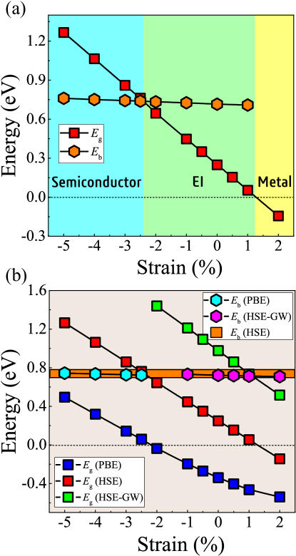
In order to be certain of our findings, we also carry out many-body GWGWKress calculations in a single-shot scheme (). The results are shown in Fig. 4(b). While unlike the HSE where the system is an EI without any strain, GW increases the from 0.25 eV (HSE) to 0.98 eV so the 2D GaAs under normal condition becomes a trivial band insulator, but turns into an EI at a modest tensile strain of 1%. Three important points are worth noting: (1) as long as , is almost a constant and its value of about 0.73 eV is also insensitive to the calculation method. (2) The given by the different methods have a rather similar slope with respect to the strain. As we increase the level of accuracy of the calculation methods, exhibits a blue shift from PBE to HSE, and then to GW. (3) Irrespective of the methods, there is always a crossing point between the and curves in Fig. 4(b). Hence, irrespective of the technical details, we conclude that while the exact is difficult to predict, it is unambiguous that all the methods used here predicts the formation of EI at modest experimental conditions.
With these results in hand, we further notice that single-layer TiS3, which has been experimentally exfoliatedIsland , also fulfills the parity requirement. Previous workDai showed that the HSE calculation is necessary to yield the consistent with the experiment for TiS3. Nevertheless, the computational cost is unaffordable at present for a fully converged solution of BSE at the HSE level for the system. Fortunately, it is revealed in Fig. 4(b) that the just weakly depends upon the calculation methods which suggests an alternative estimation of from the PBE result. Our first-principles calculations show that the (HSE level) monotonously decreases but the (PBE level) varies a little with the increase of compressive strain for the single-layer TiS3. Without strain, it is 1.16 eV vs. 0.92 eV for vs. , while it becomes 0.90 eV vs. 0.94 eV under -3% strain, indicative of the transition to EI phase. Such a moderate strain lies within an experimentally accessible regime, thus calling experimentalists for test.
In summary, we show that direct gap materials whose band-edge states possess the same parity are promising candidates for the EIs. Actually, any material with a lowest transition forbidden, regardless of direct or indirect gap, might be promising for engineering an intrinsic EI. Note that this EI principle works independent of the dimensionality. In three-dimensional bulk materials, however, the large screening often limits to be only a few or several tens of an meV, as well as making an effective tuning of and difficult. In this regard, 2D semiconductors with an appropriate band parity and a reasonable offer a unique opportunity for success. The 2D materials also hold another promise because a modest strain variation can lead to a rich phase diagram ranging from a traditional semiconductor, over an EI, to a metal, therefore potentially allowing for a device of complex functionalities to be made of purely a single material.
Acknowledgements.
Work in China was supported by the Ministry of Science and Technology of China (Grant No. 2016YFA0301001), the National Natural Science Foundation of China (Grant Nos. 51788104, 11674071, 21373015, and 11674188), the Beijing Advanced Innovation Center for Future Chip (ICFC), and Open Research Fund Program of the State Key Laboratory of Low-Dimensional Quantum Physics. Work in the US was supported by the US DOE Grant No. DESC0002623.References
- (1) D. Jérome, T. M. Rice, and W. Kohn. Phys. Rev. 158, 462 (1967).
- (2) M. Rontani and L. J. Sham, in Novel Superfluids, edited by K. H. Bennemann and J. B. Ketterson (Oxford University Press, Oxford, 2014), vol. 2, p. 423.
- (3) A. Kogar, S. Vig, M. S. Rak, A. A. Husain, F. Flicker, Y. I. Joe, L. Venema, G. J. MacDougall, T. C. Chiang, E. Fradkin, J. van Wezel, and P. Abbamonte, Science 358, 1314 (2017).
- (4) L. J. Du, X. W. Li, W. K. Lou, G. Sullivan, K. Chang, J. Kono, and R.-R. Du, Nat. Commun. 8, 1971 (2017).
- (5) H. Cercellier, C. Monney, F. Clerc, C. Battaglia, L. Despont, M. G. Garnier, H. Beck, P. Aebi, L. Patthey, H. Berger, and L. Forró, Phys. Rev. Lett. 99, 146403 (2007).
- (6) M. Cazzaniga, H. Cercellier, M. Holzmann, C. Monney, P. Aebi, G. Onida, and V. Olevano, Phys. Rev. B 85, 195111 (2012).
- (7) S. Mor, M. Herzog, D. Golež, P. Werner, M. Eckstein, N. Katayama, M. Nohara, H. Takagi, T. Mizokawa, C. Monney, and J. Stähler, Phys. Rev. Lett. 119, 086401 (2017).
- (8) Y. F. Lu, H. Kono, T. I. Larkin, A. W. Rost, T. Takayama, A. V. Boris, B. Keimer, and H. Takagi, Nat. Commun. 8, 14408 (2017).
- (9) Y. Wakisaka, T. Sudayama, K. Takubo, T. Mizokawa, M. Arita, H. Namatame, M. Taniguchi, N. Katayama, M. Nohara, and H. Takagi, Phys. Rev. Lett. 103, 026402 (2009).
- (10) B. Bucher, P. Steiner, and P. Wachter, Phys. Rev. Lett. 67, 2717 (1991).
- (11) F. X. Bronold and H. Fehske, Phys. Rev. B 74, 165107 (2006).
- (12) P. M. R. Brydon and C. Timm, Phys. Rev. B 80, 174401 (2009).
- (13) M. E. Zhitomirsky, T. M. Rice, and V. I. Anisimov, Nature (London) 402, 251 (1999).
- (14) E. Bascones, A. A. Burkov, and A. H. MacDonald, Phys. Rev. Lett. 89, 086401 (2002).
- (15) D. Varsano, S. Sorella, D. Sangalli, M. Barborini, S. Corni, E. Molinari, and M. Rontani, Nat. Commun. 8, 1461 (2017).
- (16) D. Sherrington and W. Kohn, Rev. Mod. Phys. 40, 768 (1968).
- (17) K. Rossnagel, L. Kipp, and M. Skibowski, Phys. Rev. B 65, 235101 (2002).
- (18) T. Kaneko, T. Toriyama, T. Konishi, and Y. Ohta, Phys. Rev. B. 87, 035121 (2013).
- (19) Z. Y. Jiang, Z. R. Liu, Y. C. Li, and W. H. Duan, Phys. Rev. Lett. 118, 266401 (2017).
- (20) Z. R. Liu, J. Wu, and W. H. Duan, Phys. Rev. B 69, 085117 (2004).
- (21) G. Fiori, F. Bonaccorso, G. Iannaccone, T. Palacios, D. Neumaier, A. Seabaugh, S. K. Banerjee, and L. Colombo, Nat. Nanotech. 9, 768 (2014).
- (22) X. L. Nie, S. H. Wei, and S. B. Zhang, Phys. Rev. Lett. 88, 066405 (2002).
- (23) M. C. Lucking, W. Y. Xie, D.-H. Choe, D. West, T.-M. Lu, and S. B. Zhang, Phys. Rev. Lett. 120, 086101 (2018).
- (24) J. P. Perdew, K. Burke, and M. Ernzerhof, Phys. Rev. Lett. 77, 3865 (1996).
- (25) G. Kresse and J. Furthmüller, Phys. Rev. B 54, 11169 (1996).
- (26) J. Heyd, G. E. Scuseria, and M. Ernzerhof, J. Chem. Phys. 118, 8207 (2003).
- (27) J. Heyd, G. E. Scuseria, and M. Ernzerhof, J. Chem. Phys. 124, 219906 (2006).
- (28) M. Shishkin and G. Kresse, Phys. Rev. B 74, 035101 (2006).
- (29) A. Marini, C. Hogan, M. Grüning, and D. Varsano, Comput. Phys. Commun. 180, 1391 (2009).
- (30) M. Rohlfing and S. G. Louie, Phys. Rev. B 62, 4927 (2000).
- (31) P. Giannozzi, S. Baroni, N. Bonini, M. Calandra, R. Car, C. Cavazzoni, D. Ceresoli, G. L. Chiarotti, M. Cococcioni, I. Dabo, A. D. Corso, S. de Gironcoli, S. Fabris, G. Fratesi, R. Gebauer, U. Gerstmann, C. Gougoussis, A. Kokalj, M. Lazzeri, L. Martin-Samos, N. Marzari, F. Mauri, R. Mazzarello, S. Paolini, A. Pasquarello, L. Paulatto, C. Sbraccia, S. Scandolo, G. Sclauzero, A. P. Seitsonen, A. Smogunov, P. Umari, and R. M. Wentzcovitch, J. Phys.: Condens. Matter 21, 395502 (2009).
- (32) Z. Y. Al Balushi, K. Wang, R. K. Ghosh, R. A. Vilá, S. M. Eichfeld, J. D. Caldwell, X. Y. Qin, Y.-C. Lin, P. A. DeSario, G. Stone, S. Subramanian1, D. F. Paul, R. M. Wallace, S. Datta, J. M. Redwing, and J. A. Robinson, Nat. Mater. 15, 1166 (2016).
- (33) Y. Li and X. Chen, 2D Mater. 1, 031002 (2014).
- (34) F. Tran and P. Blaha, Phys. Rev. Lett. 102, 226401 (2009).
- (35) J. O. Island, M. Barawi, R. Biele, A. Almazán, J. M. Clamagirand, J. R. Ares, C. Sánchez, H. S. J. van der Zant, J. V. Álvarez, R. D’Agosta, I. J. Ferrer, and A. Castellanos-Gomez, Adv. Mater. 27, 2595 (2015).
- (36) J. Dai and X. C. Zeng, Angew. Chem. Int. Ed. 54, 7572 (2015).