Pixel Detectors … where do we stand?
Abstract
Pixel detectors have been the working horse for high resolution, high rate and radiation particle tracking for the past 20 years. The field has spun off into imaging applications with equal uniqueness. Now the move is towards larger integration and fully monolithic devices with to be expected spin-off into imaging again. Many judices and prejudices that were around at times were overcome and surpassed. This paper attempts to give an account of the developments following a line of early prejudices and later insights.
keywords:
Tracking detectors, pixel detectors, semiconductor detectorsPACS:
29.40.Wk , 29.40.Gx1 Introduction
Pixel detectors have entered particle physics experiments in the early nineties, first with small scale devices [1, 2] and soon after with developments of detectors with o(108) pixels for the LHC experiments (see e.g. [3]). Despite early approaches with monolithic devices [4, 5, 6] so-called hybrid pixels in which pixel sensor and readout chip are separated entities, mated by employing bumping and flip-chipping technology, have been the technology of choice, in particular for applications in high rate and radiation environments [7] as at the LHC. Soon after also developments targeting imaging applications, in particular biomedical and synchrotron light X-ray imaging [8, 9] have been started, commencing their own development branches. As of today these development have culminated in very successful large scale detectors in the LHC experiments [10, 11, 12, 3] on the one hand and in imaging detectors on the other [13, 14, 15].
A bit later though, monolithic pixel detectors also reached a state of performance that made them attractive for particle and heavy ion physics experiments where low material budget plays an overwhelming role due to the low average momenta of particles emerging from the interactions. Fully monolithic pixel detectors where realised in the STAR experiment at RHIC [16] and a follow-up 10 m2 detector is in production for the ALICE Inner Tracker ITS [17]. Also for the extreme radiation and rate environment encountered at the HL-LHC so-called depleted monolithic active pixels (DMAPS) have been developed [18] [19] that are able to cope with them (section 4). As was the case for hybrid pixels monolithic imaging devices are also spinning off, targeting X-ray and synchrotron radiation applications in astrophysics, biomedical imaging, and spectroscopy. This conference has devoted an integrated workshop on SOI-pixels in particular addressing such applications [20].
Early prejudices
In order to put the developments into some perspective I have chosen to follow a personal line of some early thinking and prejudices on pixel detectors, in particular those developed for LHC rate and radiation levels. Such statements are for example:
-
-
Radiation levels at LHC and HL-LHC are tough for pixel sensors; and there is no alternative to planar pixels.
-
-
Diamond will never become a material suited for a pixel tracker.
-
-
The bulk material choice has to be p-type.
-
-
Pixel sensors from CMOS IC fabrication lines do not have sufficient performance in terms of charge collection and radiation tolerance.
-
-
A complex chip with o(109) transistors can only be done by industry, needs many years of development, and is too expensive. However, as the 250 nm technology was already radhard, the 65 nm technology will be even better.
-
-
Only hybrid pixel designs can cope with LHC conditions. Monolithic pixels will never stand the LHC rate and radiation environment.
-
-
SOI pixel technology is fine, but it is extremely difficult to get around the many challenges of shielding sensitive structures.
-
-
Silicon micropattern detectors are good for spatial resolution, but not for timing.
Much of this early thinking was wrong or has been overcome today as will be addressed in this paper.
2 Pixel sensors in high radiation environments
N- or p-type bulk
Apart from rate capability the required radiation tolerance is the dominant issue to cope with in most high energy physics experiments today. At the HL-LHC every Si lattice cell will see about 50 particles during its lifetime. The recipe developed over the years has been (i) readout at n+ electrodes (e- collection), (ii) operation at high bias voltages, (iii) a careful planning of the annealing scenario, (iv) proper electrode and guard ring design, and recently (v) to use p-substrates with n electrodes (rather than n-in-n). While there is empirical evidence for the latter [21] it became evident that details of the electrode structure and sensor thickness complicated the issue [21]. Only recently p-type silicon as a sensor material has been studied in some detail. Bombardment with hadrons (p,n,) causes damage to the silicon lattice which is independent of the type of doping. However, the effective doping concentration changes due to different effects. While in n-type silicon shallow donors (like phosphorus) are removed when a V-P complex is formed, the acceptor (boron B) abundance seems to be dominantly decreased by an interstitial BiOi complex [22, 23], decreasing the negative space charge of the bulk. For n-type material a practical and efficient mitigation has been invoked by oxygen enrichment having VO complexes competing with VP. For p-type material such an efficient cure still has to be established [24].
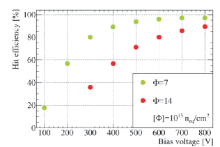
Therefore, while for LHC upgrades the change from to for LHC experiment upgrades is necessary for strip detectors, from the radiation point of view, (present pixel choice) is equally suited at least, except that for the fabrication of the latter double sided processing is needed. Hence strip and hybrid planar pixel sensors for the HL-LHC upgrades both plan on employing p-type substrates. For planar pixel detectors fig. 1(a) shows the cross section developing from the current LHC pixels (250–300 m) to thin pixel sensors (100–150); fig. 1(b) shows their performance under extreme radiation damage. Note in fig. 1(a) that the readout chip (ROC) must be placed in very close distance to parts of the sensor being under high voltage potential. Special isolation protection must be applied.

3D pixel electrodes
Very high fluences have imposed a real threat to standard pixel detector designs using planar electrodes, coped with only by thin sensors and high bias voltages (see previous section). Alternative pixel electrodes have been proposed and developed since the late 1990s [25, 26] as so-called 3D-silicon sensors featuring columnar electrode implants driven into the Si substrate perpendicular to the sensor surface (fig. 2). The smaller electrode distance than sensor thickness renders shorter drift distance and higher fields at moderate bias voltages, together resulting in an increased radiation tolerance.
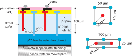
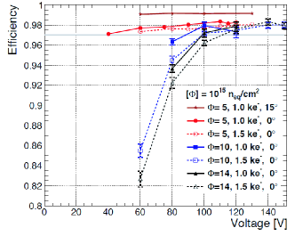
Within the ATLAS IBL detector 3D-Si pixel sensors have been proven to operate well in a running experiment [29]. After two years of operation the performance of 3D-Si pixel modules in terms of operation characteristics are on par with planar pixel modules, the latter operated with significantly higher bias [30]. Optimizations for HL-LHC [31, 28, 27] include [27] thinner sensors (100 m) on 6′′ wafers, slimmer (5 m) and more closely spaced (30 m) electrodes, and very slim or active edges. A design example [27] is shown in fig. 2(a). In addition to cost and yield advantages of single-sided processing, studies have shown that the trade-off between signal efficiency and breakdown performance favors partial depth n-columns (not extending all the way through the thickness) [32]. The performance of such designs has been shown to yield high breakdown voltages before and after irradiation [33]. The hit efficiency obtained with 3D-Si structures [34] is demonstrated in fig. 2(b).
Diamond pixels
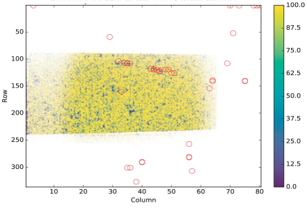
Diamond has been considered the material for radiation hard pixels due to (a) its large band gap switching off any leakage current and (b) its twice as high energy kick-off threshold (43 eV) to remove an atom from the lattice compared 25 eV for Si, mitigating lattice damage at a given fluence. However, manufacturing and cost issues in producing single crystal sensor grade material (scCVD) as well as charge collection performance and other systematic issues associated with the grain structure of polycrystalline (pCVD) diamond, have so far prevented diamond pixels to become real tracking devices in an experimental arrangement. However, large progress has been made in developing 'quasi tracker' like detectors, as for example the ATLAS Diamond Beam Monitor (DBM) consisting of four 3-layer telescopes arranged symmetrically around the beam at small forward and backward angles (see also [35]). An efficiency map [36] exhibiting also the grain structure is shown in fig. 3(a). With a mean overall efficiency of 87.6% and remaining inhomogeneities due to the grain boundaries in pCVD, the demands on a stand alone tracking device for individual particles are not yet sufficiently met. For applications, however, where robustness of response and radiation immunity (e.g. for beam monitors) plays a larger role, pCVD diamond is a suitable choice.
Sensors fabricated in CMOS production lines
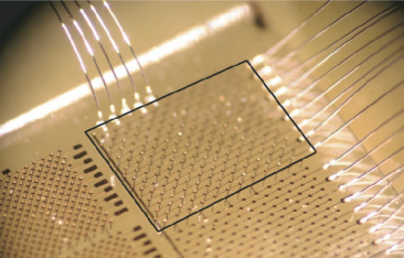
In the past high ohmic pixel sensors were fabricated by dedicated sensor production vendors. Employing high throughput chip wafer manufacturers for sensor fabrication was believed to be too risky since the HEP community is not a large market to receive sufficient attention, and that the sensor quality would generally be insufficient. On the other hand, a number of advantages are in reach as there are: (i) Large volume production lines with price and turn-around benefits, (ii) 8′′ or 12′′ wafer sizes, (iii) wafers can be purchased to come with solder bumps of mid-size pitch (), (iv) standardly available metal layers can be exploited for (a) AC coupling and (b) optimal line redistribution when connecting sensor to R/O chip, such that large and ganged pixels can be avoided (see fig. 4(a)).
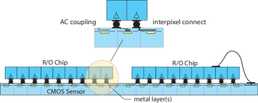
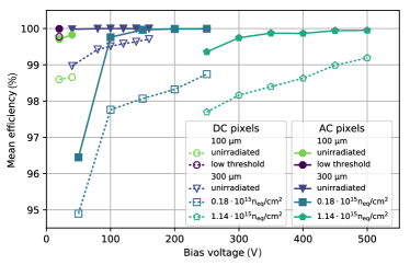
The early conception is about to change as has been successfully demonstrated for strip [39, 40] and pixel sensors [38]. Measurements on passive CMOS pixel sensors, 100 m and 300 m thick, irradiated to fluences of 1.1 neq/cm2 have shown lab and test beam performance at least equal to those of planar sensors fabricated in dedicated sensor production lines [38]. This is evident from fig. 4(b) where very high mean hit efficiency are reached for DC and particularly for AC coupled passive CMOS sensors bonded to the readout chip FE-I4 [41].
3 Pixel readout chip
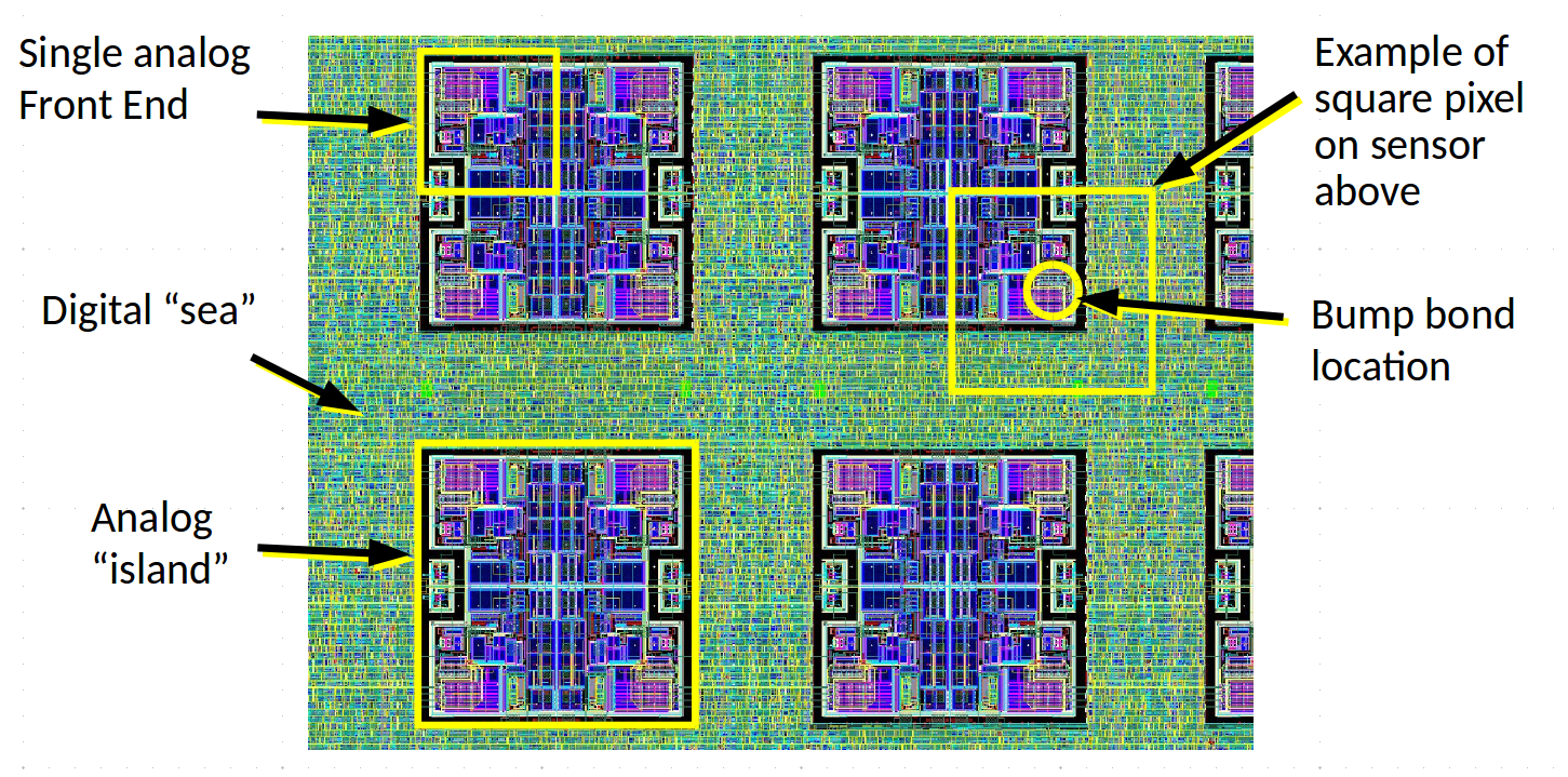
Indeed, as said in the introduction, a large and complex readout chip with o(109) transistors is a huge and costly enterprise which has been addressed by the RD53 collaboration at CERN [42]. In comparison to the chips of the previous hybrid pixel generation which were column drain architectures without (1st generation) or with (2nd generation) a local (4-pixel) cluster efficient hit storage, this 3rd generation contains architecture blocks with grouped logic enabling regional hit draining surrounded by synthesized logic, dubbed the 'digital sea' [43] and [44].
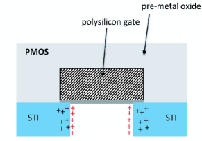
Regarding radiation it seemed that the 250 nm and 130 nm technologies have hit a sweet spot. The naive belief that smaller deep submicron technologies would be even more radhard neglected radiation induced narrow/short channel effects (RINCE and RISCE, respectively, Fig. 5(b)) as is detailed by F. Faccio’s presentation at this conference [45].
4 Monolithic Pixels
The many advantages of hybrid pixel detector face some serious drawbacks, among them the material budget and the laborious assembly of the hybrid parts. In recent years monolithic pixel approaches have strongly emerged, first by employing CMOS imaging technologies leading to so-called MAPS devices with charge collection by diffusion in the chip’s epitaxial layer [5, 6]. This technology has also found its way into HEP experiments in need for low material budget and small pixel devices, but facing lower than LHC rates, such as RICH’s STAR experiment [46, 16] and culminating in the 10 m2 pixel detector of the ALICE upgrade [17] (see also [7]).
It was believed for a long time that LHC rates and radiation levels were prohibitive for MAPS, but they could be addressed by monolithic pixels in special processes, featuring high voltage and high resistive wafers, multiple wells, and backside processing [18]. In the past four years this approach culminated in fully monolithic designs that can cope with the LHC radiation levels of above neqcm-2 (fluence) and 1 MGy (dose) as well as the corresponding particle rates. For the HL-LHC they are thus suited at least for the outer pixel layers.
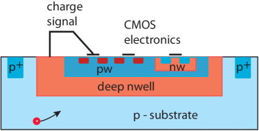
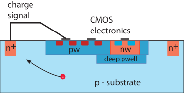
Two promising lines of actual research are currently followed: (a) large electrode designs (large fill factor, FF), where the electronics is embedded in the electrode covering a large fraction of the pixel area and (b) small electrode (small FF) designs where the collection electrode is set aside from the shielded electronics area (see also [47].) The pros and cons are obvious. While the large FF design provides short average drift distances and hence promises radiation hardness it suffers from a relatively large input capacitance to the amplifier, governed by its large area and, in addition, by the capacitance introduced between the deep p-well and the deep n-well. The latter also represents a coupling path between electronics and sensor such that transient digital signals coupling into the sensor must be prevented by dedicated circuitry. The small FF approach offers all the benefits imposed by the small ( fF) input capacitance, suffers, however, from larger average drift distances for the same pixel area. A process modification [48] (see also [47]), strengthening the lateral drift by sideward depletion, improves the charge collection towards the small collection electrode.
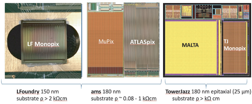
Both approaches have been matured by intensive prototyping R&D leading to large ( cm2) fully monolithic pixel chips with full readout architectures suitable for LHC rates as shown in fig. 7. The large FF chips are under test, the small FF design is currently fabricated (see also [49]).
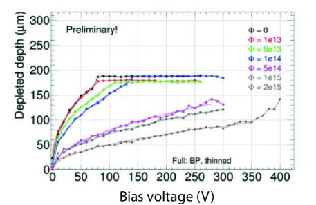
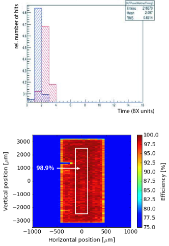
The main results for large FF devices are summarized in fig. 8: (i) Depletion depths in excess of 100 are reached even after neqcm-2 (fig. 8(a)); (ii) gain decreases and noise increases remain below 10% and 30%, respectively, after radiation doses of 1 MGy; (iii) the timing requirements after irradiation are close to being met after a correction; and (iv) the hit efficiency after neqcm-2 is still close to 99% at a noise occupancy of .
SOI pixels
A full workshop within this conference is devoted to SOI pixels (see for example [20] and references therein). Mastering complex device variations in this so-called fully-depleted SOI technology the groups managed to fabricate powerful detection devices for many application areas: particle tracking with sub-m resolutions (FPIX and SOFIST), X-ray imaging (INTPIX), X-ray astro (XRPIX, SOIPIX-PDD), synchrotron radiation (SOPHIAS), far infrared (cryogenic), biomedical counting (CNTPIX), and ion spectroscopy (MALPIX). A full account is given elsewhere at this conference. Previously existing issues like the back-gate effect, coupling between circuit and sensor, and radiation (TID) issues have been cured by several variants of buried well and nested well arrangements. The present devices are radiation hard to TIDs of 100 kGy.
Regarding SOI pixels for LHC radiation levels, it should be mentioned that promising prototyping has been done [51] using partially depleted SOI, for which the back-gate and other effects do largely not exist due to shielding wells in the electronics layer.
5 Fast timing with pixels
Sub-ns to ps timing was believed to be very difficult with silicon detectors. So-called low gain avalanche diodes, having mm2 size patterns, have been developed to cope with this challenge (see also [52] and [53]). In order to minimize time fluctuations in the signal generation process, an amplification structure is realized by a p+ implantation right underneath the n++ electrode (fig. 9(a)). The fast signal is governed by fast e/h movements in high fields of thin detectors plus large slew rates () from amplified holes moving away from the readout electrode [54]. Gains below 50 are targeted in order to avoid amplification excess noise. The structure needs a homogeneous weighting field such that small pixels are not easily realized.

The time resolution has several contributions [59]:
The terms represent time walk, noise jitter, non-uniform charge depositions along a track, position dependent signal distortion, and digitisation. The first two contributions can be made small when large slew rates are achieved.
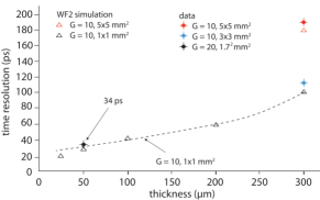
The results of this R&D are encouraging as shown in fig. 9(b) comparing data and simulations as a function of sensor thickness. In ATLAS and CMS proposals exist to employ LGADs for some timing applications for the HL-LHC upgrade. The main concern currently is the radiation tolerance since the gain varies strongly with radiation fluence due to acceptor removal in the relatively highly doped p+ layer of the multiplication region.
6 Imaging with Hybrid Pixels
As mentioned in the introduction, the hybrid pixel developments made for particle tracking shortly afterwards entered X-ray imaging for biomedical (e.g. MEDIPIX [60]) or synchrotron light applications (see also [61]). The first big detectors addressing signals with huge dynamic range (1 - 105) have come into live. Examples are among others the series of developments at PSI called EIGER (500 k pixels, 75 m pitch, photon counting, 23 kHz frame rates), MÖNCH (charge integrating, 25 pixel pitch, low noise, low energies) [62], and JUNGFRAU (charge integrating, 75 pixel pitch, dynamic gain switching) [63] for the SLS and for SWISSFEL, with which a step function in synchrotron light imaging is achieved. For the EUROPEAN XFEL first pictures of the adaptive gain imaging pixel detector AGIPD [64] have been recorded.
Also in imaging applications monolithic pixels are now taking an important role, as can for example by seen be the 'Double SOI' pixel detector presented at this conference [65].
7 Conclusions
Pixel detectors have paved the way of high resolution, high rate, and high radiation devices indispensable from particle tracking and imaging experiments. The path first laid by hybrid pixel detectors is now followed into monolithic devices and devices tuned for high timing resolution, at first again for tracking. For sure imaging applications will follow.
Acknowledgments
The author would like to thank the organizers for their kind invitation. This work was supported in parts by the Deutsche Forschungsgemeinschaft DFG, grant number WE 976/4-1, by the German Ministry BMBF under grant number 05H15PDCA9, and by the H2020 project AIDA-2020, GA no. 654168, and by the H2020 project STREAM, GA no. 675587.
References
- [1] E. H. M. Heijne et al. A 1006 element hybrid silicon pixel detector with strobed binary output. IEEE Trans. Nucl. Sci., 39:654–661, 1992.
- [2] K. H. Becks et al. The DELPHI pixels. Nucl. Instr. and Meth., A386:11–17, 1997.
- [3] L. Rossi, P. Fischer, T. Rohe, and N. Wermes. Pixel Detectors: From Fundamentals to Applications. Springer, Berlin, Heidelberg, 2006.
- [4] Walter Snoeys, James Plummer, Geert Rosseel, Chye Huat Aw, Chris Kenney, and Sherwood Parker. First beam test results from a monolithic silicon pixel detector. Nucl. Instrum. Meth., A326:144–149, 1993.
- [5] B. Dierickx, G. Meynants, and D. Scheffer. Near 100 fill factor CMOS active pixel. In Proc. SPIE – Int. Soc. Opt. Eng. (USA), volume 3410, pages 68–76, 1998.
- [6] R. Turchetta et al. A monolithic active pixel sensor for charged particle tracking and imaging using standard VLSI CMOS technology. Nucl. Instr. and Meth. A, 458:677–689, 2001.
- [7] Maurice Garcia-Sciveres and Norbert Wermes. A review of advances in pixel detectors for experiments with high rate and radiation. 2017.
- [8] M. Campbell, E. H. M. Heijne, Gerrit Jan Meddeler, E. Pernigotti, and W. Snoeys. A Readout chip for a 64 x 64 pixel matrix with 15 bit single photon counting. IEEE Trans. Nucl. Sci., 45:751–753, 1998.
- [9] P. Fischer, J. Hausmann, M. Overdick, B. Raith, N. Wermes, L. Blanquart, V. Bonzom, and P. Delpierre. A Counting pixel readout chip for imaging applications. Nucl. Instr. and Meth., A405:53–59, 1998.
- [10] G. Aad et al. ATLAS pixel detector electronics and sensors. JINST, 3:P07007, 2008.
- [11] H.C. Kastli et al. CMS barrel pixel detector overview. Nucl. Instr. and Meth. A, 582:724, 2007.
- [12] P. Chochula et al. The ALICE silicon pixel detector. Nucl. Phys., A715:849–852, 2003. [,693(2003)].
- [13] Rafael Ballabriga, Michael Campbell, and Xavier Llopart. Asic developments for radiation imaging applications: The medipix and timepix family. Nucl. Instr. and Meth., A878:10–23, 2018.
- [14] S. Redford et al. Calibration status and plans for the charge integrating JUNGFRAU pixel detector for SwissFEL. JINST, 11(11):C11013, 2016.
- [15] P. Göttlicher et al. The adaptive gain integrating pixel detector (AGIPD): A detector for the European XFEL. development and status. In Proceedings, 2009 IEEE Nuclear Science Symposium and Medical Imaging Conference (NSS/MIC 2009): Orlando, Florida, October 25-31, 2009, pages 1817–1820, 2009.
- [16] J. Schambach et al. A MAPS Based Micro-Vertex Detector for the STAR Experiment. In Physics Procedia, volume 66, pages 514–519, 2015.
- [17] B Abelev et al. Technical Design Report for the Upgrade of the ALICE Inner Tracking System. J. Phys., G41:087002, 2014.
- [18] I. Peric. A novel monolithic pixelated particle detector implemented in high-voltage CMOS technology. Nucl. Instr. and Meth. A, 582:876–885, 2007.
- [19] N. Wermes. Depleted CMOS pixels for LHC proton-proton experiments. Nucl. Instr. and Meth. A, A824:483–486, 2016.
- [20] K. Arai. High Resolution SOI Pixel Detector, 2018. Presentation given at this Conference.
- [21] Michael Moll. Recent advances in the development of radiation tolerant silicon detectors for the super-LHC. In Astroparticle, particle and space physics, detectors and medical physics applications. Proceedings, 11th International Conference on Advanced Technology and Particle Physics, ICATPP 11, Como, Italy, October 5-9, 2009, pages 101–110, 2009.
- [22] Alexandra Junkes, E. M. Donegani, and C. Neubüser. Energy dependence of proton radiation damage in Si-sensors. In Proceedings, 21st Symposium on Room-Temperature Semiconductor X-ray and Gamma-ray Detectors (RTSD 2014): Seattle, WA, USA, November 8-15, 2014, page 7431260, 2016.
- [23] E. Donegani. Energy-Dependent Proton Damage in Silicon. PhD thesis, U Hamburg, 2017. http://www.iexp.uni-hamburg.de/groups/pd/?q=theses/energy-dependent-proton-damage-silicon.
- [24] M. Moll. Displacement damage in silicon detectors for High Energy Physics. In Proceedings of Radecs 2017, Geneva, Switzerland, Oct. 2017. to appear in IEEE Trans. Nucl. Sci.
- [25] C. Kenney, S. Parker, and J. Segal. 3d - a proposed new architecture for solid-state radiation detectors. Nucl. Instr. and Meth. A, 395:328–343, 1997.
- [26] C. Da Via et al. 3D active edge silicon sensors: Device processing, yield and QA for the ATLAS-IBL production. Nucl. Instr. and Meth. A, 699:18–21, 2013.
- [27] G.-F. Dalla Betta et al. Development of New 3D Pixel Sensors for Phase 2 Upgrades at LHC. 2016. http://inspirehep.net/record/1501528/files/arXiv:1612.00608.pdf.
- [28] J. Lange et al. 3D silicon pixel detectors for the High-Luminosity LHC. JINST, 11(11):C11024, 2016.
- [29] ATLAS. Operation experience wuth the IBL, 2018.
- [30] A. La Rosa. The ATLAS Insertable B-Layer: from construction to operation. JINST, 11(12):C12036, 2016.
- [31] G.-F. Dalla Betta et al. Development of a new generation of 3D pixel sensors for HL-LHC. Nucl. Instrum. Meth., A824:386–387, 2016.
- [32] G.-F. Dalla Betta. 3D-Si sensor design. private communication, 2017.
- [33] D.M.S. Sultan et al. First Production of New Thin 3D Sensors for HL-LHC at FBK. In Proceedings, 18th International Workshop on Radiation Imaging Detectors (IWORID 2016): Barcelona, Spain, July 3-7, 2016, 2016.
- [34] J. Lange, S. Grinstein, M. Manna, G. Pellegrini, D. Quirion, S. Terzo, and D. Vázquez Furelos. Radiation hardness of small-pitch 3D pixel sensors up to HL-LHC fluences. In International conference on Technology and Instrumentation in Particle Physics’17 (TIPP2017) Beijing, China, May 22-26, 2017, 2017.
- [35] H. Kagan. Diamond detector technology; status and perspectives, 2018. Presentation given at this Conference.
- [36] J. Janssen. Test beam results of ATLAS DBM pCVD diamond detectors using a novel threshold tuning method. JINST, 12(03):C03072, 2017.
- [37] L. Bäni et al. Diamond detectors for high energy physics experiments. JINST, 13(01):C01029, 2018.
- [38] D. L. Pohl, T. Hemperek, F. Hügging, J. Janssen, H. Krüger, A. Macchiolo, N. Owtscharenko, I. Caicedo Sierra, L. Vigani, and N. Wermes. Radiation hard pixel sensors using high-resistive wafers in a 150 nm CMOS processing line. 2017. preprint arXiv:1702.04953 [physics.ins-det], 2017.
- [39] M. Dragicevic et al. Results from a beam test of silicon strip sensors manufactured by Infineon Technologies AG. Nucl. Instr. and Meth., A765:1–6, 2014.
- [40] T. Bergauer, M. Dragicevic, A. König, J. Hacker, and U. Bartl. First thin AC-coupled silicon strip sensors on 8-inch wafers. Nucl. Instr. and Meth., A830:473–479, 2016.
- [41] M. Garcia-Sciveres et al. The FE-I4 pixel readout integrated circuit. Nucl. Instr. and Meth. A, 636:155, 2011.
- [42] RD53. The RD53 Collaboration at CERN, 2018. weblink https://rd53.web.cern.ch/RD53/.
- [43] N. Demaria et al. Recent progress of RD53 Collaboration towards next generation Pixel Read-Out Chip for HL-LHC. JINST, 11(12):C12058, 2016.
- [44] M. Garcia-Sciveres. Advances in pixel elecronics for experiments with high rate and radiation, 2018. Presentation given at this Conference.
- [45] F. Faccio et al. FEAST2: A Radiation and Magnetic Field Tolerant Point-of-Load Buck DC/DC Converter. In Radiation Effects Data Workshop (REDW), 2014 IEEE, 2015.
- [46] G. Contin et al. The MAPS-based vertex detector for the STAR experiment: Lessons learned and performance. Nucl. Instr. and Meth. A, 831:7–11, 2016.
- [47] W. Snoeys. Monolithic CMOS sensors for high energy physics, 2018. Presentation given at this Conference.
- [48] W. Snoeys et al. A process modification for CMOS monolithic active pixel sensors for enhanced depletion, timing performance and radiation tolerance. Nucl. Instrum. Meth., A871:90–96, 2017.
- [49] H. Pernegger. Monolithic Pixel Development in TowerJazz 180 nm CMOS for the outer pixel layers in the ATLAS experiment, 2018. Presentation given at this Conference.
- [50] I. Mandić, V. Cindro, A. Gorišek, B. Hiti, G. Kramberger, M. Zavrtanik, M. Mikuž, and T. Hemperek. Charge collection properties of irradiated depleted CMOS pixel test structures. 2018.
- [51] T. Hemperek, T. Kishishita, H. Krüger, and N. Wermes. A Monolithic Active Pixel Sensor for ionizing radiation using a 180 nm HV-SOI process. Nucl. Instr. and Meth. A, 796:8–12, 2015.
- [52] H. Sadrozinski. Timing Resolution Measurements on Utra-fast Silicon Detectors, 2018. Presentation given at this Conference.
- [53] H.F.W. Sadrozinski, A. Seiden, and N. Cartiglia. 4D tracking with ultra-fast silicon detectors. Rept. Prog. Phys., 81(2):026101, 2018.
- [54] H. F. W. Sadrozinski et al. Ultra-fast silicon detectors. Nucl. Instr. and Meth., A730:226–231, 2013.
- [55] N. Cartiglia et al. Design optimization of ultra-fast silicon detectors. Nucl. Instr. and Meth., A796:141–148, 2015.
- [56] H.F.-W. Sadrozinski et al. Ultra-fast silicon detectors (UFSD). Nucl. Instr. and Meth. A, 831:18–23, 2016.
- [57] N. Cartiglia et al. Beam test results of a 16 ps timing system based on ultra-fast silicon detectors. Nucl. Instrum. Meth., A850:83–88, 2017. preprint arXiv:1608.08681 [physics.ins-det], 2016.
- [58] N. Cartiglia et al. Tracking in 4 dimensions. Nucl. Instrum. Meth., A845:47–51, 2017.
- [59] N. Cartiglia et al. The 4D pixel challenge. JINST, 11(12):C12016, 2016.
- [60] Rafael Ballabriga, Michael Campbell, and Xavier Llopart. Asic developments for radiation imaging applications: The medipix and timepix family. Nucl. Instrum. Meth., A878:10–23, 2018.
- [61] G. Carini. Overview of the X-ray detectors for photon science experiments, 2018. Presentation given at this Conference.
- [62] M. Ramilli et al. Measurements with MÖNCH, a 25 μm pixel pitch hybrid pixel detector. JINST, 12(01):C01071, 2017.
- [63] A. Mozzanica et al. Characterization results of the JUNGFRAU full scale readout ASIC. JINST, 11(02):C02047, 2016.
- [64] A. Allahgholi et al. The adaptive gain integrating pixel detector. JINST, 11(02):C02066, 2016.
- [65] T. Miyoshi. Development and performance of double SOI pixel sensors, 2018. Presentation given at this Conference.