Origin and Evolution of Surface Spin Current in Topological Insulators
Abstract
The Dirac surface states of topological insulators offer a unique possibility for creating spin polarized charge currents due to the spin-momentum locking. Here we demonstrate that the control over the bulk and surface contribution is crucial to maximize the charge-to-spin conversion efficiency. We observe an enhancement of the spin signal due to surface-dominated spin polarization while freezing-out the bulk conductivity in semiconducting Bi1.5Sb0.5Te1.7Se1.3 below . Detailed measurements up to room temperature exhibit a strong reduction of the magnetoresistance signal between , which we attribute to the thermal excitation of bulk carriers and to the electron-phonon coupling in the surface states. The presence and dominance of this effect up to room temperature is promising for spintronic science and technology.
Three-dimensional (3D) topological insulators (TIs) emerge as a result of band inversion due to strong spin-orbit (SO) coupling. These band inversions lead to the appearance of topologically protected gapless surface states, which have one spin state per momentum at the Fermi surface (Fig. 1a).Xia et al. (2009); Hasan and Kane (2010); Pesin and MacDonald (2012); Ando (2013) The spins of carriers in TI surface states are locked perpendicular to their momenta (spin-momentum locking, SML) enabling the creation of spin polarization by applying a charge current (Fig. 1b).Ando (2013); Hasan and Kane (2010) These unique spin polarized surface states of TIs due to SML have been coupled to ferromagnetic contacts for creating giant spin transfer effects and for potentiometric detection of the current-induced spin polarization Li et al. (2014); Ando et al. (2014); Tang et al. (2014a); Liu et al. (2015); Tian et al. (2015); de Vries et al. (2015); Li et al. (2016a); Yang et al. (2016) even up to room temperature.Dankert et al. (2015)
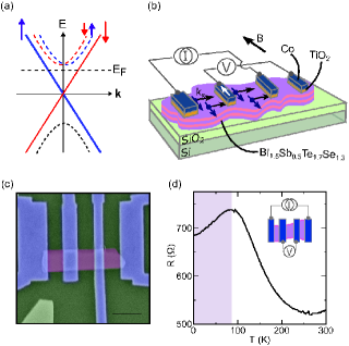
However, the interpretation of the results has remained challenging due to mixed contributions from the topological and trivial surface states on top of a bulk background conduction in prototype TIs such as Bi2Se3, Bi2Te3 and Sb2Te3, which have naturally-occurring Se and Te vacancies resulting in unintentional doping.Pesin and MacDonald (2012) These bulk carriers reduce the current-induced spin polarization in two ways: (i) by decreasing the fraction of the current flowing on the spin-momentum-locked surface states, and (ii) by allowing the coupling between the topological surface states and the non-topological bulk and surface states. In particular, phonon-mediated surface-bulk coupling can lead to interband scattering between various spin-orbit states (dashed lines in Fig. 1a),Hong et al. (2012); Hammar and Mark (2000); Yazyev, Moore, and Louie (2010); Datzer et al. (2017) which affects the detected surface spin polarization. These bulk-related problems have been improved upon by developing semiconducting bulk TIs (BixSb1-x)2Te3 and Bi1.5Sb0.5Te1.7Se1.3 (BSTS), where the surface state transport dominates at low temperature with parallel bulk conduction at high temperatures.Ren et al. (2011) However, only few studies reported the potentiometric detection of SML in such bulk semiconducting TIs, and were limited to cryogenic temperatures below .Ando et al. (2014); Tang et al. (2014a) The electrical investigation of the SML phenomenon up to room temperature in such low doped TIs is crucial for the basic understanding of the influence of surface state and bulk band contribution to the detected magnetoresistance (MR) signal.
Here we study the surface spin polarization in BSTS with ferromagnetic tunnel contacts between . The semiconducting bulk nature of BSTS thin films enables us to investigate SML in a surface-dominated transport regime at low temperatures and a surface-bulk coexistent (SBC) conduction regime at high temperatures. These results provide an understanding of the origin and evolution of SML signals with temperature as well as the contribution of bulk bands and topological surface states.
Device and electrical characterization of BSTS. The devices were prepared by depositing ferromagnetic (FM) tunnel contacts (Co/TiO2) on exfoliated BSTS flakes on a SiO2/Si substrate (Fig. 1b and 1c, as well as Appendix Part A1).Dankert et al. (2014, 2015) The tunnelling characteristics of the contacts are presented in Appendix Fig. A2. The temperature dependence of BSTS channel resistance in a flake with a thickness shows an increasing channel resistance from room temperature to , and then decreasing below (Fig. 1d). The increase in resistance when cooling down is expected for semiconducting BSTS flakes stemming from a parallel bulk contribution, whereas the reduction in resistance below indicates a freezing out of the charge carriers in the semiconducting bulk and increasingly dominating surface transport.Xia et al. (2013) The freezing out of the bulk carrier states in our BSTS is further supported by Hall measurements showing a steady decrease of the charge carrier concentration with temperature (see Appendix Fig. A3). This indicates a remaining surface transport channel with higher mobility compared to the semiconducting bulk at low temperature. Using the measured charge carrier concentration and Fermi energy distribution, we can calculate the Fermi level to be within the band gap and about below the conduction band edge Kondou et al. (2016).
Magnetotransport and quantum oscillations. Magnetotransport measurements in BSTS show a weak anti-localization (WAL) behaviour up to indicating a strong SO coupling (Appendix Fig. A4). Using the Hikami-Larkin-Nagaoka (HLN) model, we can fit the conductivity correction () of the surface states with
| (1) |
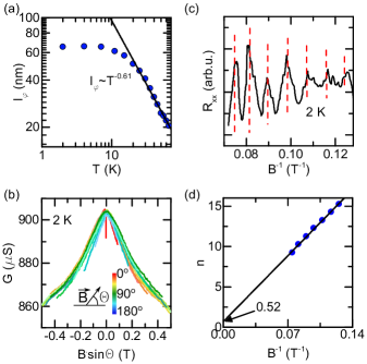
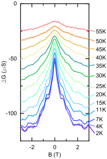
where represents the digamma function, is the phase coherence length, and represents the dimensionality factor of the quantum systemHikami, Larkin, and Nagaoka (1980). The temperature dependence of the phase coherence length above (Fig. 2a) indicates a 2D system with dominant phonon scattering (), which is comparable to previous reports on surface-dominant BSTS Xia et al. (2013) validating the usage of the HLN model. Figure 2b shows the measured conductivity at for an angle from to plotted against the perpendicular magnetic field component . The angle independence of this normalized WAL signal together with its short phase coherence length and its characteristic temperature dependence confirms the 2D surface states as the dominating transport channel at cryogenic temperatures.
In high magnetic field measurements, we also observed Shubnikov-de Haas (SdH) quantum oscillations in the longitudinal resistance with a perpendicular magnetic field up to at . Figure 2c shows the oscillations as a function of the inverse magnetic field, where the parabolic magnetoresistive background has been subtracted. The respective fan diagram correlates the inverse magnetic fields at the maxima directly to different Landau levels (Fig. 2d), where slope is the oscillation frequency and offset is defined by the Berry phase Novoselov et al. (2005). We extract yielding , which is expected for the Dirac electrons in the topological surface states. Consequently, we can use the Onsager’s relation to calculate the surface charge carrier concentrationAndo (2013) , which is comparable to the charge carrier concentration extracted from Hall measurements (see Appendix Part A3). Since Hall measurements probe both bulk and surface transport, the identical charge carrier concentration from Hall and SdH measurements at implies a vanishing bulk background at low temperatures. The temperature and angle dependence of the WAL and the Berry phase of the SdH oscillations are clear evidence for a surface-dominated transport at low temperature.
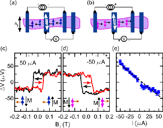
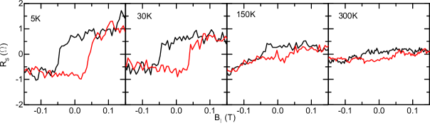
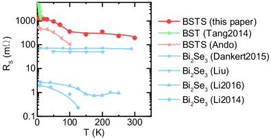
Electrical detection of SML. BSTS with a dominant surface transport is ideal to study the contribution to the magnetoresistance signal due to SML. Figure 3a shows the measurement principle on a multi-terminal BSTS device. By applying a charge current we generate a spin polarization () in the BSTS surface states due to SML. This net spin polarization beneath the FM tunnel contact (Co/TiO2) is detected as a voltage signal depending on parallel or anti-parallel alignment of the FM and the spin orientation. Sweeping the in-plane magnetic field, the magnetization of the FM detector is switched with respect to yielding a step in the voltage signal. An up- and down-sweep of the magnetic field results in a hysteretic switching presented in Fig. 3c, as measured on a BSTS flake of thickness at by applying a DC current of . Similarly, the spin polarization in the BSTS surface states can be flipped by inverting the current direction ( in Fig. 3b), resulting in a reversed spin signal (Fig. 3d) Dankert et al. (2015). Measuring the full bias range, we observe a linear dependence of the spin signal (Fig. 3e), as expected, since the spin density scales linearly with the current density Hong et al. (2012). However, the strong spin-orbit coupling in the TI as well as stray fields at the magnetic contacts can yield contributions from Rashba states,Pesin and MacDonald (2012) spin Hall or stray Hall effects,de Vries et al. (2015); Appelbaum, Tinkey, and Li (2014) mimicking a SML signal. Previously, such spurious effects have been ruled out by several control experiments using angle,Dankert et al. (2015) gate Liu et al. (2015) and carrier dependent Li et al. (2016b, a) measurements. In particular the stray Hall effect is strongly charge carrier type dependent, whereas the spin locking is not. Therefore, we studied Sb2Te3, a known p-type TI, to confirm the sign of the detected MR signal (see Appendix Part A6). The observed SML signal matches our data reported here on BSTS, as well as previous studies on Bi2Se3 and BST Liu et al. (2015); Dankert et al. (2015); Tang et al. (2014a); Ando et al. (2014), which confirms the signal origin stemming from the SML in the TI surface states. Additionally, we observe an enhanced spin resistance up to in BSTS at low temperature, which is orders of magnitude higher than aforementioned spin Hall and stray Hall effects Liu et al. (2015). Furthermore, such a high is also at least one order of magnitude higher than previously reported SML results on metallically doped TIs Li et al. (2014); Dankert et al. (2015), comparable to reports on BSTSAndo et al. (2014), and can be attributed to the reduced number of bulk carriers at low temperature.
In order to understand the origin of the enhancement of the signal at low temperature, we carried out a detailed temperature dependence measurement of the magnetoresistance. We observed a clear MR switching up to room temperature, which decreases drastically when warming up from and levels off in the SBC regime (Fig. 4a and Appendix Fig. A5). Previous reports on potentiometric measurements on BSTS show a similar temperature dependence Ando et al. (2014); Ren et al. (2011), however, in a low temperature range. In contrast, on highly doped TIs, different studiesDankert et al. (2015); Mellnik et al. (2014); Liu et al. (2015); Jamali et al. (2015); Li et al. (2014); Tang et al. (2014b) showed only a weak temperature dependence over large temperature ranges (see also Appendix Fig. A6).
In our case, the change in the temperature dependence at around coincides with the transition from surface to SBC transport behaviour (Fig. 1d). Below the activation gap, the number of bulk carriers and the inelastic scattering rate of surface states increase exponentially with temperature Saha and Garate (2014); Liu et al. (2015). This temperature dependence becomes polynomial when the temperature exceeds the activation gap, as seen in Fig. 4a Dankert, Dulal, and Dash (2013); Dankert et al. (2015). This indicates that the detected signal stems from SML in the surface states partly suppressed by a temperature dependent surface-bulk scattering and thermally activated bulk charge carriers Yazyev, Moore, and Louie (2010); Hong et al. (2012); de Vries et al. (2015).
Next, we fit the temperature-dependent resistance shown in Fig. 1d to a two-channel transport model. In this model, the thermally activated bulk conductance is given by , where is the Boltzmann constant, is the high-temperature bulk resistivity and is the activation gap between the Fermi level and the closest bulk states. Similarly, the surface state conductance reads
| (2) |
The surface resistance , with the low temperature residual resistance and an exponential increase with temperature of the scattering from surface to bulk states (), is dominated by non-linear phonon contribution parameters ( and ) at low temperatures (below the Bloch-Grüneisen temperature ) Giraud, Kundu, and Egger (2012) and the linear electron-phonon scattering parameter for . From the fitting, one may extract the fraction of the current that flows on the surface states, . This fraction decreases rapidly from 100% at low temperature to about 30% at , beyond which it remains almost constant up to (Fig. 4b). In contrast to previous transport modelsXu et al. (2014), this behaviour matches our experimentally observed resistance change and theoretical expectations of a thermally activated dominant bulk conduction in thin-film TIs well.
Finally, we can estimate the spin resistance , due to SML induced by a current yielding the surface spin polarization , which can be expressed as
| (3) |
where is the polarization of the FM detector and is the ballistic resistanceHong et al. (2012). The former has been found in previous studies to have an upper limit of for our Co/TiO2 contactsKamalakar et al. (2015); Dankert et al. (2015). The ballistic conductance equals the quantum of conductance multiplied by the number of propagating modes , where is the width of the conductance channel. The Fermi wave number can be derived from the 2D charge carrier concentration as .Dankert et al. (2015) Using Eq. (3) and the surface charge carrier concentrations measured in SdH and Hall measurements, we calculate a current-induced surface spin polarization , which is almost constant within the error margins over the full temperature range (Fig. 4b) and twice as high as previously reported Hsieh et al. (2009); Li et al. (2014); Yazyev, Moore, and Louie (2010); Dankert et al. (2015). The deviation from the optimal originates from spin-orbit entanglement in the topological surface states Yazyev, Moore, and Louie (2010), as well as the possible occurrence of non-topological surface states at the Fermi level Bahramy et al. (2012); Bianchi et al. (2010). Optimising the crystal growth and doping could yield a lower bulk conduction and hence a high surface spin signal under ambient conditions, which would present a serious competition for ferromagnetic contacts in spintronic applications.
In summary, we have presented the electrical detection of spin polarized surface currents due to SML on BSTS by FM tunnel contacts over a broad temperature range up to . High quality semiconducting BSTS crystals and FM tunnel contacts allowed the observation of a spin signal of up to , which is at least one order of magnitude higher than previously reported results on metallically doped TIs in the same temperature range Dankert et al. (2015); Li et al. (2016b). The large magnitude of the signal and its sign, combined with quantum transport measurements prove clearly the SML originating from surface states at low temperature. Furthermore, we observe a strong temperature dependence of the SML signal up to , thereafter remaining constant up to room temperature. A two-channel transport model considering thermally activated bulk carriers and surface-to-bulk scattering confirms an almost temperature independent surface spin polarisation . This elucidates the influence of the bulk conduction and scattering mechanisms that suppress the detected SML signal, whilst still observable up to room temperatureDankert et al. (2015).
Acknowledgement The authors acknowledge financial supports from the European Union’s Horizon 2020 research and innovation programme under grant agreement No 696656 (Graphene Flagship), EU FlagEra project (from Swedish Research council VR No. 2015-06813), Swedish Research Council VR project grants (No. 2016-03658), Graphene center and the AoA Nano program at Chalmers University of Technology. The authors also acknowledge the support of colleagues at the Quantum Device Physics Laboratory and Nanofabrication Laboratory at Chalmers University of Technology.
References
- Xia et al. (2009) Y. Xia, D. Qian, D. Hsieh, L. Wray, A. Pal, H. Lin, A. Bansil, D. Grauer, Y. S. Hor, R. J. Cava, and M. Z. Hasan, Nat. Phys. 5, 398 (2009).
- Hasan and Kane (2010) M. Z. Hasan and C. L. Kane, Rev. Mod. Phys. 82, 3045 (2010).
- Pesin and MacDonald (2012) D. Pesin and A. H. MacDonald, Nat. Mater. 11, 409 (2012).
- Ando (2013) Y. Ando, J. Phys. Soc. Jpn. 82, 102001 (2013).
- Li et al. (2014) C. H. Li, O. M. J. van ’t Erve, J. T. Robinson, Y. Liu, L. Li, and B. T. Jonker, Nat. Nanotechnol. 9, 218 (2014).
- Ando et al. (2014) Y. Ando, T. Hamasaki, T. Kurokawa, K. Ichiba, F. Yang, M. Novak, S. Sasaki, K. Segawa, Y. Ando, and M. Shiraishi, Nano Lett. 14, 6226 (2014).
- Tang et al. (2014a) J. Tang, L.-T. Chang, X. Kou, K. Murata, E. S. Choi, M. Lang, Y. Fan, Y. Jiang, M. Montazeri, W. Jiang, Y. Wang, L. He, and K. L. Wang, Nano Lett. 14, 5423 (2014a), http://dx.doi.org/10.1021/nl5026198 .
- Liu et al. (2015) L. Liu, A. Richardella, I. Garate, Y. Zhu, N. Samarth, and C.-T. Chen, Phys. Rev. B: Condens. Matter Mater. Phys. 91 (2015), 10.1103/PhysRevB.91.235437.
- Tian et al. (2015) J. Tian, I. Miotkowski, S. Hong, and Y. P. Chen, Sci. Rep. 5, 14293 (2015).
- de Vries et al. (2015) E. K. de Vries, A. M. Kamerbeek, N. Koirala, M. Brahlek, M. Salehi, S. Oh, B. J. van Wees, and T. Banerjee, Phys. Rev. B Condens. Matter 92, 201102 (2015).
- Li et al. (2016a) C. H. Li, O. M. J. van ’t Erve, Y. Y. Li, L. Li, and B. T. Jonker, Sci. Rep. 6, 29533 (2016a).
- Yang et al. (2016) F. Yang, S. Ghatak, A. A. Taskin, K. Segawa, Y. Ando, M. Shiraishi, Y. Kanai, K. Matsumoto, A. Rosch, and Y. Ando, Phys. Rev. B: Condens. Matter Mater. Phys. 94, 075304 (2016).
- Dankert et al. (2015) A. Dankert, J. Geurs, M. V. Kamalakar, S. Charpentier, and S. P. Dash, Nano Lett. 15, 7976 (2015).
- Hong et al. (2012) S. Hong, V. Diep, S. Datta, and Y. P. Chen, Phys. Rev. B Condens. Matter 86, 085131 (2012).
- Hammar and Mark (2000) P. R. Hammar and J. Mark, Phys. Rev. B: Condens. Matter Mater. Phys. 61, 7207 (2000).
- Yazyev, Moore, and Louie (2010) O. V. Yazyev, J. E. Moore, and S. G. Louie, Phys. Rev. Lett. 105, 266806 (2010).
- Datzer et al. (2017) C. Datzer, A. Zumbülte, J. Braun, T. Förster, A. B. Schmidt, J. Mi, B. Iversen, P. Hofmann, J. Minár, H. Ebert, P. Krüger, M. Rohlfing, and M. Donath, Phys. Rev. B Condens. Matter 95, 115401 (2017).
- Ren et al. (2011) Z. Ren, A. A. Taskin, S. Sasaki, K. Segawa, and Y. Ando, Phys. Rev. B Condens. Matter 84 (2011), 10.1103/PhysRevB.84.165311.
- Dankert et al. (2014) A. Dankert, L. Langouche, M. V. Kamalakar, and S. P. Dash, ACS Nano 8, 476 (2014).
- Tu et al. (2014) N. H. Tu, Y. Tanabe, K. K. Huynh, Y. Sato, H. Oguro, S. Heguri, K. Tsuda, M. Terauchi, K. Watanabe, and K. Tanigaki, Appl. Phys. Lett. 105, 063104 (2014).
- Fert (2008) A. Fert, Rev. Mod. Phys. 80, 1517 (2008).
- Dash et al. (2009) S. P. Dash, S. Sharma, R. S. Patel, M. P. de Jong, and R. Jansen, Nature 462, 491 (2009).
- Dankert, Dulal, and Dash (2013) A. Dankert, R. S. Dulal, and S. P. Dash, Sci. Rep. 3, 3196 (2013).
- Xia et al. (2013) B. Xia, P. Ren, A. Sulaev, P. Liu, S.-Q. Shen, and L. Wang, Phys. Rev. B Condens. Matter 87, 085442 (2013).
- Kondou et al. (2016) K. Kondou, R. Yoshimi, A. Tsukazaki, Y. Fukuma, J. Matsuno, K. S. Takahashi, M. Kawasaki, Y. Tokura, and Y. Otani, Nat. Phys. (2016), 10.1038/nphys3833.
- Hikami, Larkin, and Nagaoka (1980) S. Hikami, A. I. Larkin, and Y. Nagaoka, Progr. Theoret. Phys. 63, 707 (1980).
- Novoselov et al. (2005) K. S. Novoselov, A. K. Geim, S. V. Morozov, D. Jiang, M. I. Katsnelson, I. V. Grigorieva, S. V. Dubonos, and A. A. Firsov, Nature 438, 197 (2005).
- Appelbaum, Tinkey, and Li (2014) I. Appelbaum, H. N. Tinkey, and P. Li, Phys. Rev. B: Condens. Matter Mater. Phys. 90 (2014), 10.1103/PhysRevB.90.220402.
- Li et al. (2016b) C. H. Li, O. M. J. van ’t Erve, S. Rajput, L. Li, and B. T. Jonker, Nat. Commun. 7, 13518 (2016b).
- Mellnik et al. (2014) A. R. Mellnik, J. S. Lee, A. Richardella, J. L. Grab, P. J. Mintun, M. H. Fischer, A. Vaezi, A. Manchon, E.-A. Kim, N. Samarth, and D. C. Ralph, Nature 511, 449 (2014).
- Jamali et al. (2015) M. Jamali, J. S. Lee, J. S. Jeong, F. Mahfouzi, Y. Lv, Z. Zhao, B. K. Nikolić, K. A. Mkhoyan, N. Samarth, and J.-P. Wang, Nano Lett. 15, 7126 (2015), http://dx.doi.org/10.1021/acs.nanolett.5b03274 .
- Tang et al. (2014b) J. Tang, L.-T. Chang, X. Kou, K. Murata, E. S. Choi, M. Lang, Y. Fan, Y. Jiang, M. Montazeri, W. Jiang, Y. Wang, L. He, and K. L. Wang, Nano Lett. 14, 5423 (2014b).
- Saha and Garate (2014) K. Saha and I. Garate, Phys. Rev. B Condens. Matter 90, 245418 (2014).
- Giraud, Kundu, and Egger (2012) S. Giraud, A. Kundu, and R. Egger, Phys. Rev. B Condens. Matter 85, 035441 (2012).
- Xu et al. (2014) Y. Xu, I. Miotkowski, C. Liu, J. Tian, H. Nam, N. Alidoust, J. Hu, C.-K. Shih, M. Z. Hasan, and Y. P. Chen, Nat. Phys. 10, 956 (2014).
- Kamalakar et al. (2015) M. V. Kamalakar, C. Groenveld, A. Dankert, and S. P. Dash, Nat. Commun. 6, 6766 (2015).
- Hsieh et al. (2009) D. Hsieh, Y. Xia, D. Qian, L. Wray, J. H. Dil, F. Meier, J. Osterwalder, L. Patthey, J. G. Checkelsky, N. P. Ong, A. V. Fedorov, H. Lin, A. Bansil, D. Grauer, Y. S. Hor, R. J. Cava, and M. Z. Hasan, Nature 460, 1101 (2009).
- Bahramy et al. (2012) M. S. Bahramy, P. D. C. King, A. de la Torre, J. Chang, M. Shi, L. Patthey, G. Balakrishnan, P. Hofmann, R. Arita, N. Nagaosa, and F. Baumberger, Nat. Commun. 3, 1159 (2012).
- Bianchi et al. (2010) M. Bianchi, D. Guan, S. Bao, J. Mi, B. B. Iversen, P. D. C. King, and P. Hofmann, Nat. Commun. 1, 128 (2010).
Appendix
A1 Fabrication and characterization
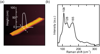
The Bi1.5Sb0.5Te1.7Se1.3 flakes were exfoliated from a bulk crystal, using the conventional Scotch tape cleavage technique, onto a clean SiO2 ()/highly doped n-type Si substrate. The crystal was obtained from Miracrys, grown from a melt using a high vertical Bridgeman method Dankert et al. (2015). The flakes were identified using optical microscopy and the flake thickness, uniformity, and material quality was analyzed with atomic force microscopy and Raman spectroscopy, respectively (Fig. A1a and A1b). This revealed homogeneous thick flakes with widths of about and a characteristic Raman spectrum for BSTS Tu et al. (2014). Electrodes were patterned by electron beam lithography. The contact deposition was performed in an ultra-high vacuum electron beam evaporator after an in situ surface cleaning using low power argon ion plasma for . Electrodes with widths and channel length of are used. As contact material, we used TiO2/Co for the detection of spin-momentum locking. The TiO2 tunnel barrier was deposited by electron beam evaporation and in situ oxidation using a pure oxygen atmosphere. The BSTS devices were measured with a Quantum Design Physical Property Measurement System (PPMS) with resistivity option using direct current (DC).
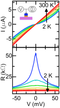
A2 Characterization of ferromagnetic tunnel junctions
The tunnelling properties of the ferromagnetic (FM) tunnel contacts are characterized in a three-terminal measurement configuration (Fig. A2). The current-voltage characteristics exhibit a non-linear behaviour typical for tunnelling transport. Furthermore, the temperature dependence shows an increase of the resistance by only a factor of 5 with decrease in temperature indicating a good quality TiO2 tunnel barrier on the BSTS flakes Jonsson-Akerman2000-ib.
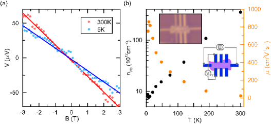
A3 Temperature dependence of carrier mobility and concentration
Hall measurements were performed on a Bi1.5Sb0.5Te1.7Se1.3 channel between and (Fig. A3). By applying a perpendicular magnetic field the Hall voltage across the channel width is detected, allowing us to extract the 2D charge carrier concentration and mobility . Fig. A3 shows a low at , comparable to the surface charge carrier concentration extracted from Shubnikov-de Haas measurements (see main manuscript), and increasing with temperature, due to thermally excited carriers from the bulk. The mobility at room temperature is about , and increases to at . This behaviour matches well with an intrinsically low doped semiconductor freeze-out in the bulk at low temperatures with a remaining charge carrier concentration stemming from the surface states at .
A4 Weak anti-localization
The quantum transport properties of BSTS were measured by sweeping an out-of-plane magnetic field while measuring the lateral channel resistance. We observe a correction of the magnetoresistance as expected for strong SO coupled materials resulting in weak anti-localization up to (Fig. A4).
A5 Temperature dependence of SML signals
A6 Comparison of SML signals
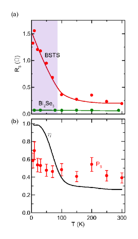
The amplitude and the temperature dependence of the SML signal in our BSTS devices are compared in Fig. A6 with literature values since the first report of electrical SML detection by Li2014Li et al. (2014), various studies on Bi2Se3 (LiuLiu et al. (2015), Dankert2015Dankert et al. (2015), Li2016Li et al. (2016b)), in (Bi0.53Sb0.47)2Te3(Tang2014Tang et al. (2014a)) and Bi1.5Sb0.5Te1.7Se1.3(this paper and AndoAndo et al. (2014)). The SML signal voltage is compared as spin resistance. Our SML signal amplitude is at least one order of magnitude higher than reported in metallically doped Bi2Se3. The temperature dependence of our BSTS sample spans the full temperature range of . Only two other studies on metallic Bi2Se3 cover a similar rangeDankert et al. (2015); Li et al. (2016b). Below , the strong signal increase in our measurement matches well the results on semiconducting BSTSAndo et al. (2014) and BSTTang et al. (2014a). All studies on metallic Bi2Se3 show a weak temperature dependence, whereas the variation presented in studies with low detected spin potential splittingLi et al. (2014, 2016b) may be due to other influences, and the temperature dependence is also negligible compared to BSTS.
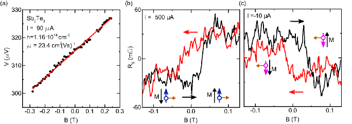
A7 Spin-momentum locking in p-type TI Sb2Te3
The stray fields at the magnetic contacts can yield stray Hall effects, which can appear similar to the SML signal. However, such spurious signals are strongly charge carrier dependent and change sign when switching from electron to hole transport. In contrast, the spin polarisation of the SML does not depend on the charge carriers, since the locking as well as the momentum are opposite for holes and electrons. We studied Sb2Te3, a known p-type TI, to verify the origin of the measured signal. Figure A7a shows the Hall measurement in Sb2Te3, which exhibits a majority hole carrier concentration of . The observed SML signal for positive (Fig. A7b) and negative (Fig. A7c) bias current shows the typical hysteretic switching and matches our data reported here on BSTS, as well as previous studies on Bi2Se3 and BST Liu et al. (2015); Dankert et al. (2015); Tang et al. (2014a); Ando et al. (2014), which confirms the signal origin stemming from the SML in the TI surface states.