An induced annealing technique for SiPMs neutron radiation damage
Abstract
The use of Silicon Photo-Multipliers (SiPMs) has become popular in the
design of High Energy Physics experimental apparatus with a growing
interest for their application in detector area where a significant
amount of non-ionising dose is delivered. For these devices, the main
effect caused by the neutron fluence is a linear increase of the leakage
current.
In this paper, we present a technique that provides a
partial recovery of the neutron damage on SiPMs by means of an
Electrical Induced Annealing. Tests were performed, at the temperature of 20°C, on a sample of
three SiPM arrays () of 6 mm2 cells with
pixel sizes: two from Hamamatsu and one from
SensL. These SiPMs have been exposed to neutrons generated by the Elbe Positron Source facility (Dresden),
up to a total fluence of n1MeV-eq/cm2. Our techniques allowed to reduced the leakage
current of a factor ranging between 15-20 depending on the overbias
used and the SiPM vendor. Because, during the process the
SiPM current can reach O(100 mA), the sensors need to be operated in a condition that
provides thermal dissipation. Indeed, caution must be used when applying this kind of
procedures on the SiPMs, because it may damage permanently the devices themself.
1 Introduction
A Silicon Photo-Multiplier (SiPM) is a novel semiconductor
photo-detector composed by a matrix of pixels operating few volts
above the breakdown voltage (Geiger-Mode Avalanche
Photo-Diode). Distinctive features of such technology are: single
photon detection capability, high gain 106 and good time
resolution ( 1 ns) [1]. In addition SiPMs present
small size and customisable granularity, insensitivity to magnetic
fields and are relatively un-expensive. For these reasons several
current and planned High Energy Physics experiments employ SiPMs in
their experimental setup [4, 5]. A growing interest
exists in their application when a high level of non-ionizing dose is
expected to be delivered to the SiPMs.
Different studies showed a
correlation between the bulk defects in the Silicon structure due to
the radiation damage and the deterioration of the photo-detector
performances [6, 7].
Hadrons and high energy leptons can produce point defects as well
as cluster related defects in the photo-detector active volume. In
particular, neutrons travelling within the Silicon lattice induce many
displacements of Silicon atoms that, at the end of the path, form a
disordered agglomeration of atoms called
cluster [8]. From the
macroscopic point of view, some of these defects act as charge
carriers generator centers, producing an increase of dark noise.
The current state of the art technology does not provide any method to fully recover neutron
induced damage in Silicon based photo-detectors. Thermal annealing can
partially recover the neutron induced damage, as shown in
Ref. [9], where after several days of thermal
treatment at different temperatures, the dark current got reduced by a factor of about 10.
Our tests reported in the next sections indicate that an important
recovery of the SiPM damage can be achieved also by means of an electrical
induced annealing in few minutes of treatment. Two different methods have been tested: a direct
and an inverse polarization of the SiPM using a non conventional over
voltage - larger than the usual 5 V limit indicated by several
vendors [1, 2]. We believe that this technique may combine two effects:
the thermal annealing induced by heating the Silicon lattice
and the presence of a strong electric field to re-order the atoms in
the Silicon lattice displaced by the neutron-induced bulk
damage [10].
2 Experimental setup
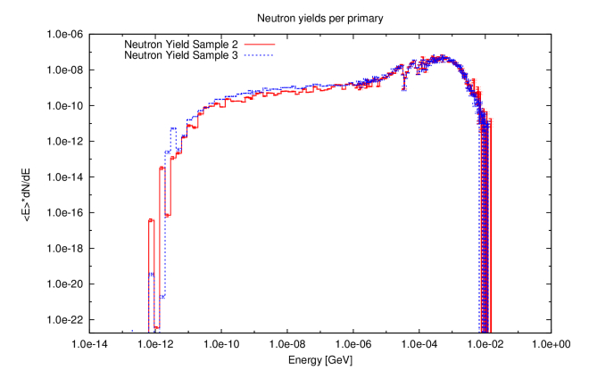
The measurements described in this paper were performed at the Silicon Detector Facility of the Fermi National accelerator Laboratory 222http://www.fnal.gov. Two different sets of SiPM arrays were studied: Hamamatsu [1] and SensL [2]. A sample from each vendor has been exposed to neutrons generated by the Elbe Positron Source facility (Dresden), up to a total fluence of n1MeV-eq/cm2 [3]. The average energy of neutrons produced has been estimated by a full FLUKA simulation; the spectrum, Figure 1, is well centred around 1 MeV.
The tests described in this paper has been conducted after 3 months from the irradiation. During most of the time, the SiPMs were kept
at room temperature of about 20 °C and in a dark box.
These SiPMs consist of a 2×3 array of 6×6 mm2 monolithic cells with pixel sizes of 50 m. Both SiPM arrays have a custom design,
developed for the electromagnetic calorimeter of the Mu2e experiment [11], [12].
To improve the thermal dissipation capabilities compared to commercial designs333Hamamastu and SensL, private
communication, they have been built with a thermal resistance of about .
The experimental setup consisted of:
-
•
light tight thermal chamber TestEquity Model 140 [13];
-
•
power supply PLH250 [14] to bias the SiPMs and measure their current;
-
•
Cu plate, 3 mm thick, used as thermal support for the SiPMs;
-
•
3 PT1000 [15] thermistors used to measure the temperatures of the SiPM and of the Cu support.
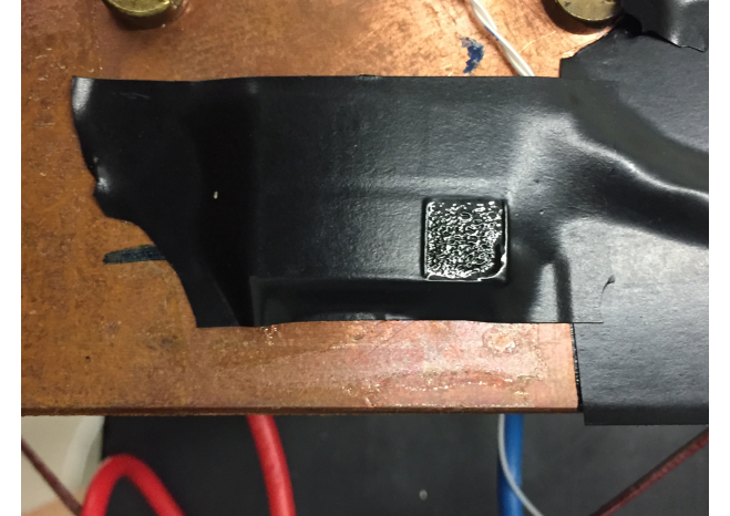
Figure 2 shows a picture of the Cu support with the PT1000, used to measure the temperature of the support, and one SiPM array plugged in. All the tests were performed inside a thermal chamber at a temperature of 20 °C.
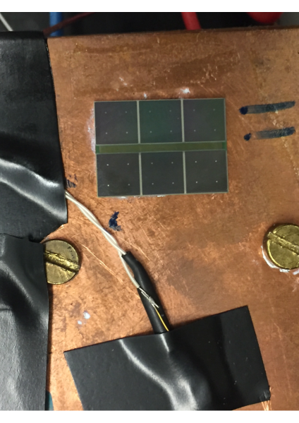
This setup allowed us to monitor the temperature of the SiPM active region and of the Cu support during all the measurements and bias the SiPM with a current limitation of few hundreds mA. A second PT1000 sensor was placed on the top of the silicon resin of the SiPMs; the third PT1000 sensor was used to check that the temperature drop on the pin-side of the SiPM was within 2 °C with respect to the one measured on the active region.
3 SiPM recovery measurements
Two different configurations for biasing the SiPMs were tested: direct
and inverse polarization using an over-voltage larger than 5 V.
So, we
define:
-
•
as the direct voltage, positive voltage applied between anode and cathode;
-
•
as the reverse over voltage with respect to the breakdown voltage, , positive voltage applied between cathode and anode;
-
•
as the photo-detector current during the annealing procedures;
-
•
Idark as the leakage current measured in the standard reverse configuration of the SiPM at the operation voltage + 3 V.
All the results shown in the following are relative to the Idark at this operational voltage point. At each annealing step, the determination of Idark has been done stopping the annealing, carrying the device at 20 °C with the thermal chamber and then measuring the current.
3.1 Induced annealing in direct polarization
Figure 3 shows the results obtained with one cell of a Hamamatsu SiPM array polarized in direct configuration at = 10 V. The Idark shows an exponential trend with a decay time of s and a constant current term = 5.2 444Fit function used: .. A reduction of in Idark after min of direct polarization was achieved.
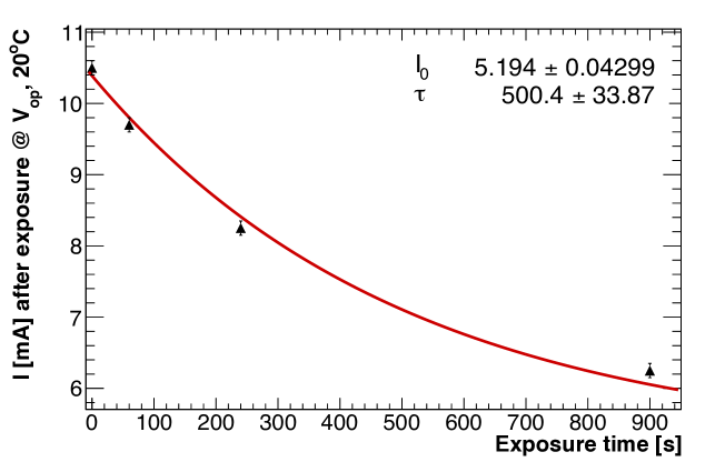
In this configuration the SiPM was generating a of mA, corresponding to a power of W, that is the power needed to recover the damage of a factor of about 2.
3.2 Induced annealing in reverse polarization
To quote the performance of the recovery method in inverse polarization two different settings of over voltage were tested. Both Hamamatsu and SensL SiPMs have been checked in this configuration. Figure 4 shows the Idark variation as a function of the exposure time for a Hamamatsu SiPM. The first four measurements were taken at = 10 V, then we improved the recovery by increasing the over voltage up to = 14 V. After about 13 min at the described conditions, the SiPM Idark reached about mA that corresponds to a reduction of a factor of 10 when compared to the starting value. Finally, we tried to increase the over-voltage up to = 17 V, but at this value the SiPM got broken.
The measured during this operation was 130 (186) mA for
a of 10 (14) V, corresponding to a dissipated
power of about 8 (12) W. The temperature measured on the SiPM active
region with the PT1000 was °C.
After the learning phase, we
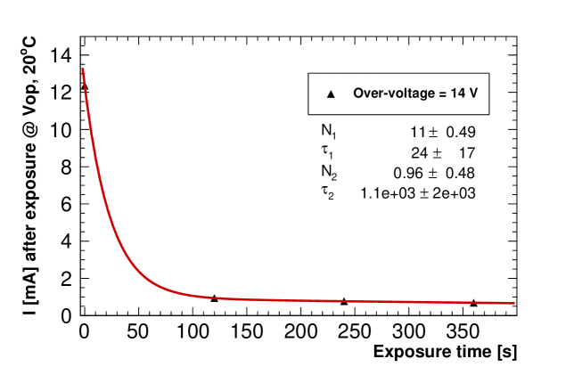
tested another Hamamatsu SiPM cell of the same device setting at 14 V. Figure 5 shows the
results of the Idark measurement operated every 2 min; from the fit555Fit function used: .
we observe that a rapid reduction of the leakage current occurs with a of the order of 25 seconds . After about 6
min of electrical annealing, a total reduction of a factor 15 on the
leakage current was observed, thus indicating a good agreement with the previous test done on the same
SiPM model.
A similar test has been carried out also for the SensL device [2]. Figure 6 shows the measured Idark for two different settings of 666The breakdown voltage of the SensL SiPM at 20 °C is 24.87 V [2].: 5 and 8 V. After 22 min we measured on overall reduction factor on Idark (from 40.2 to 2.5 mA).
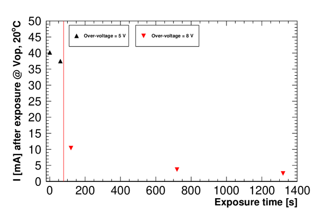
Unfortunately after 22 min the SiPM got unplugged from the Cu plate, reached a temperature larger than 200 °C and got broken. Figure 7 shows the localization of the heating induced by the over voltage condition on the single cell under bias.
During the annealing treatment, we have measured a
current of 200 (400) mA for of 5 (8)
V, corresponding to a dissipated power of about 6 (13) W. The
temperature measured on the SiPM active region was °C.
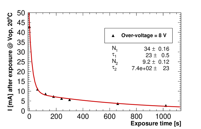
We repeated the measurement on another cell of the same device
at = 8 V. Figure 8 shows the Idark variation as a function of the exposure time; also in this case,
we observe that a rapid reduction of the leakage current occurs with a of the order of 25 seconds, consistent with the value observed in Figure 5. After
min the Idark was reduced from 42.9 to 2.7 mA that
is compatible with the reduction observed in the previous test.
4 Comparison between induced and thermal annealing
To understand if the observed reduction of Idark was due only to the
related thermal annealing, we exposed the SiPM to high temperatures at
. Since the breakdown voltage of SiPMs changes in an inversely proportional way
with the temperature following a rule of about 0.1%/°C, during the test we have adjusted
the breakdown voltage with respect to the temperature of the test. For this test we used a different cell of
the Hamamatsu SiPM array. We started keeping the SiPM at
80 °C for 19 min, then increased the temperature up to
120 °C, following the procedures explained in [9]. Results are summarised in Table 1.
| SiPM T [oC] | Exposure time [s] | Idark [mA] |
|---|---|---|
| 20 0.5 | 0 | 12.33 0.01 |
| 80 0.5 | 1120 | 9.93 0.01 |
| 120 0.5 | 600 | 9.50 0.01 |
In 30 minutes, the thermal annealing alone provided a recovery of about 25% that is much smaller than the one observed with electrical induced annealing in a much shorter time.
5 Conclusions
We have presented an electrical induced annealing technique that
allows to partially recover neutron damage of SiPM. Tests of such a
technique were performed on two different sets of SiPM arrays from
Hamamatsu and SensL. The benefit of the observed method is that it
allows to partially recover (up to a factor 15-20) the bulk damage in
the SiPM exposed to a neutron fluence of , thus improving
the results one may get with the conventional thermal annealing. A remarkable recovery related
to high temperature annealing is presented in [16], where
results of few days of annealing at +250 °C, using
forward bias with the SiPM current reaching 10 mA, are shown.
By comparison, the biggest advantage of our technique resides in the possibility to be used in an installed detector “in situ” with an application of few minutes.
In particular, we have observed that a rapid reduction of the leakage current occurs with a of the order of 25 seconds.
However, since during this process the
SiPM current can reach O(100 mA), the sensors need to be operated in a condition that
provides thermal dissipation. This precaution will avoid the sensors heating up to breaking
temperatures or damage permanently the device hosting the sensors.
Acknowledgments
This work was supported by the EU Horizon 2020 Research and Innovation Program under the Marie Sklodowska-Curie Grant Agreement No. 690385. The authors are grateful to many people for the successful realisation of the tests. In particular, we thank Dr. Adam Para, for providing us a necessary and well equipped facility at SiDet, Fermilab.
References
- [1] Hamamatsu, TSV MPPC datasheet, http://www.nuclear.gla.ac.uk/~jrma/A2/Tagger/NewFPD/SiPMT/KSX-I50014-E_S12642%20Series%20%283mm%E2%96%A1-TSV%E3%83%BCArray%29.pdf, Accessed: 2018-03-12.
- [2] SensL, SiPM datasheet, http://www.eqphotonics.de/cms/cms/upload/datasheets/PB-SensL%20Product%20Summary_IEEE.pdf, Accessed: 2017-09-2.
- [3] M. Cordelli and others, Neutron irradiation test of Hamamatsu, SensL and AdvanSiD UV-extended SiPMs, JINST (2018), vol. 13, 03, T03005.
- [4] L. Bartoszek et al., Mu2e Technical Design Report, 3rd ed. arXiv:1501.05241 [physics.ins-det], 2014.
- [5] N. Strobbe, The upgrade of the CMS hadron calorimeter with silicon photomultipliers, JINST, 12, 01, c01080, 2017.
- [6] Yu. Musienko et al., Radiation damage in silicon photomultipliers exposed to neutron radiation, JINST, 12, 07, c07030, 2017.
- [7] J.R. Srour, C.J. Marshall and P.W. Marshall, Review of Displacement Damage Effects in Silicon Devices, IEEE Transactions on Nuclear Science, 50, 653-670, 2003.
- [8] I. Pintiliea, G. Lindstroem, A. Junkesand and E. Fretwurs, Radiation Induced Point and Cluster-Related Defects with Strong Impact to Damage Properties of Silicon Detectors,
- [9] E. Garutti,Yu. Musienko, Radiation damage of SiPMs, NIM A 926, 69 - 84, 2019.
- [10] Claude Leroy and Pier-Giorgio Rancoita, Particle interaction and displacement damage in silicon devices operated in radiation environments, Reports on Progress in Physics, 70, 4, 493, 2007.
- [11] N. Atanov et al., Design and status of the Mu2e electromagnetic calorimeter, IEEE 65, 2073 - 2080, 2018.
- [12] N. Atanov et al., The Mu2e e.m. Calorimeter: Crystals and SiPMs Production Status, IEEE 67, 978 - 982, 2020.
- [13] TESTEQUITY web page, https://www.testequity.com/static/49/, Accessed: 2018-03-12.
- [14] PLH250 power supply datasheet, http://resources.aimtti.com/datasheets/AIM-PLH+PLH-P_series_DC_power_supplies_data_sheet-Iss1A.pdf, Accessed: 2018-03-12.
- [15] PT1000 datasheet, http://www.keb.com.tw/Files/Other/PDF/Data%20Sheet-PT1000-RW.pdf, Accessed: 2018-03-12.
- [16] T. Tsang, et al., Neutron radiation damage and recovery studies of SiPMs, JINST, 11, 12, P12002, 2016.