Broadband loop gap resonator for nitrogen vacancy centers in diamond
Abstract
We present an S-band tunable loop gap resonator (LGR) providing strong, homogeneous, and directionally uniform broadband microwave (MW) drive for nitrogen-vacancy (NV) ensembles. With 42 dBm of input power, the composite device provides drive field amplitudes approaching 5 G over a circular area mm2 or cylindrical volume mm3. The wide 80 MHz device bandwidth allows driving all eight NV Zeeman resonances for bias magnetic fields below 20 G. For pulsed applications the device realizes percent-scale microwave drive inhomogeneity; we measure a fractional root-mean-square inhomogeneity and a peak-to-peak variation over a circular area of 11 mm2, and and over a larger 32 mm2 circular area. We demonstrate incident MW power coupling to the LGR using multiple methodologies: a PCB-fabricated exciter antenna for deployed compact bulk sensors and an inductive coupling coil suitable for microscope-style imaging. The inductive coupling coil allows for approximately steradian combined optical access above and below the device, ideal for envisioned and existing NV imaging and bulk sensing applications.
I Introduction
The nitrogen-vacancy (NV) defect center in diamond is employed in a number of wide-ranging applications from quantum information processing Gaebel et al. (2006); Dutt et al. (2007) to tests of fundamental physics Waldherr et al. (2011); Hensen et al. (2016) to quantum sensing and metrology. In particular, NV-based quantum sensors have demonstrated utility in a broad variety of modalities, including magnetometry Taylor et al. (2008), electrometry Dolde et al. (2011); Chen et al. (2017), nanoscale NMR Devience et al. (2015); Kehayias et al. (2017); Bucher et al. (2017), single proton and single protein detection Sushkov et al. (2014); Lovchinsky et al. (2016), thermometry Neumann et al. (2013); Kucsko et al. (2013), time-keeping Hodges et al. (2013), and more Barry et al. (2016); Laraoui et al. (2015); Tetienne et al. (2017). Each of these applications takes advantage of one or more principal features of the NV center: all-optical initialization and readout van Oort, Manson, and Glasbeek (1988); Nizovtsev et al. (2003), long coherence time under ambient conditions Balasubramanian et al. (2008); Bar-Gill et al. (2013); Myers, Ariyaratne, and Jayich (2017); Bauch et al. (2018), nanoscale size Degen (2008); Maletinsky et al. (2012), or fixed crystallographic axes Maertz et al. (2010); Clevenson et al. (2018); Schloss et al. (2018). However, with notably few exceptions Wickenbrock et al. (2016); Akhmedzhanov et al. (2017), all NV applications rely on the ability to coherently manipulate the NV ground-state spin via resonant microwave (MW) driving. A number of these applications additionally require generation of strong and uniform MW fields over large areas ( mm2) or volumes ( mm3) Le Sage et al. (2013); Glenn et al. (2017); Fu et al. (2014); Wolf et al. (2015); Clevenson et al. (2015), a difficult task that benefits significantly from improvements to standard MW delivery methods. In this work, we discuss the design considerations for a suitable MW delivery mechanism, fabricate a hole-and-slot type loop gap resonator (LGR), and evaluate its performance for NV applications.
Multi-channel imagers and highly sensitive, single-channel bulk sensors are two examples of application modalities that benefit significantly from large detection areas and volumes, respectively. In the case of multi-channel imagers, increasing the detection area extends the measurement field-of-view, whereas for bulk sensors, increasing the detection volume can considerably enhance measurement sensitivity. For example, the shot-noise-limited sensitivity of an NV magnetometer is approximately given by Taylor et al. (2008)
| (1) |
where is the number of NV sensors, is the duration of the measurement, is the measurement contrast, is the number of photons collected per NV per measurement, is the Bohr magneton, is the ground state NV- Landé g-factor, and is the reduced Planck constant. The magnetic sensitivity can be improved by increasing , achievable through higher NV density or larger detection volumes. However, NV ensemble coherence times, which limit the optimal measurement time , depend inversely on NV density Taylor et al. (2008). As a result, there is a practical upper bound on the NV density after which further sensitivity enhancements are attained by increasing the detection volume. For application modalities such as those discussed above, the MW field requires both high power and uniformity in order to achieve high-fidelity quantum state manipulation over the full measurement region.
Standard approaches to applying MW drive to NV ensembles or other solid state spin systems include shorted coaxial loops Clevenson et al. (2015); Chipaux et al. (2015), microstrip waveguides Andrich et al. (2017); Zhang et al. (2016), coplanar waveguides Zhang et al. (2018), and other coaxial transmission line approaches Mrózek et al. (2015). While such broadband approaches allow abitrary drive frequency, the lack of resonant enhancement forces a compromise between the volume addressed (assuming a fixed homogeneity is required) and MW field strength, denoted . Planar lumped-element resonators such as split-ring resonators Bayat et al. (2014); Zhang et al. (2016), planar-ring resonators Sasaki et al. (2016); Twig, Suhovoy, and Blank (2010), omega resonators Twig, Suhovoy, and Blank (2010); Horowitz et al. (2012); Horsley et al. (2018); Simpson et al. (2017), and patch antennas Zhang et al. (2016) forego the flexibility of broadband solutions in favor of resonantly enhanced magnetic fields, thus enabling MW driving over larger regions. For example, the split-ring resonator presented by Bayat et al. achieves a MW field strength of G and a fractional root-mean-square inhomogeneity of over a mm2 area Bayat et al. (2014). However, such planar structures are ill-suited to providing good homogeneity away from the plane of fabrication. The community has addressed this shortcoming by employing a variety of three-dimensional resonators. Enclosed metallic cavity resonators Rose et al. (2017), enclosed dielectric resonators Breeze et al. (2017); Le Floch et al. (2016); Creedon et al. (2015), open dielectric resonators Kapitanova et al. (2017), and certain three-dimensional lumped element resonators Angerer et al. (2016) all allow for good homogeneity over large volumes but unfortunately offer little to no optical access. As all-optical initialization and readout is a primary benefit for many solid-state spin systems, including NV-diamond Doherty et al. (2013), such a trade-off is incompatible with many existing and envisioned applications Schirhagl et al. (2014).
To address this current shortcoming we present a three-dimensional tunable loop gap resonator. The design is based on the anode block of a hole-and-slot-type cavity magnetron and, similar to certain devices discussed above, utilizes resonant enhancement to achieve the desired MW drive strengths over large areas (50 mm2) or volumes (250 mm3). The design has an open geometry; for interrogation volumes centered within the LGR, approximately half of the solid angle remains optically accessible. Importantly, for currently semi-standardized commercial diamond plates (2-4.5 mm side lengths with 0.5 mm thickness) this solution allows maximal access to the diamond’s large front and back faces. The open access, good homogeneity, and high fields over the 8 mm diameter by 5 mm thickness cylindrical volume make the device well-suited both for wide-field magnetic imaging—applicable to studies of living systems Kucsko et al. (2013); Le Sage et al. (2013); Barry et al. (2016); Davis et al. (2018), early earth rocks or meteorites Glenn et al. (2017); Fu et al. (2014), single cells Glenn et al. (2015), electronic devices Simpson et al. (2016), etc.—and for single-channel bulk sensing Acosta et al. (2009); Wolf et al. (2015); Clevenson et al. (2015); Chatzidrosos et al. (2017); Barry et al. (2016) targeting geosurveying, magnetic anomaly detection, space weather monitoring, etc.
II Loop Gap Resonator Design and Fabrication
A standard hole-and-slot LGR with outer loops may be approximated as coupled LC resonators oscillating in tandem Wood, Froncisz, and Hyde (1984). Circulating currents around the central and outer loops create a total inductance , given by Froncisz and Hyde (1982); Froncisz, Oles, and Hyde (1986); Wood, Froncisz, and Hyde (1984)
| (2) |
where and denote the inductance of the central loop and of a single outer loop, respectively. Similarly, the narrow capacitive gaps create a total capacitance C, which is given by Froncisz and Hyde (1982); Froncisz, Oles, and Hyde (1986); Wood, Froncisz, and Hyde (1984)
| (3) |
where and are the capacitive gap side wall area and separation, respectively. The resonant frequency of the LGR is therefore given by
| (4) |
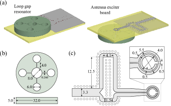
In practice, the central loop diameter is set to 5-10 mm, corresponding to the typical size of a diamond plate, whereas is limited by practical machining tolerances and by physically available materials. The capacitive gap area is constrained by the dual LGR design objectives of (i) maintaining optical accessibility, which limits the thickness of the LGR device, and (ii) bounding above the target resonant frequency in order to allow for further tuning via shims (discussed below). Additionally, while increasing the number of loops and gaps can improve uniformity Piasecki and Froncisz (1993), this approach results in a denser mode spectrum Froncisz and Hyde (1982) and increases the likelihood of cross-mode excitations deleteriously altering the field distribution within the central loop. As a compromise, our design employs outer loops [Fig. 1(b)], thus allowing for sufficient uniformity while locating the closest eigenmode more than 1.5 GHz below the TE01 eigenmode.
The LGR detailed in this work consists of a central loop of radius mm surrounded by symmetrically arranged outer loops of radius mm, as shown in Fig. 1(b). The outer loops return magnetic flux to the central loop and therefore oscillate antisymmetrically with the central loop (180∘ out of phase). The side walls of the capacitive gaps are separated by m. With these dimensions, Eqns. 2 and 3 predict nH and pF respectively, resulting in an expected resonant frequency for the naked air-gapped LGR of GHz, approximately 1.2 GHz above the NV resonance frequencies. For comparison, the measured for the air-gapped resonator is in the 4.6-4.9 GHz range.
The LGR resonant frequency is additionally tuned by inserting and translating dielectric shims in the LGR’s capacitive gaps, thereby increasing total capacitance until overlaps the NV resonance frequencies as desired. As shimming material, we employ 200 m thick C-plane sapphire, which is commercially available in semiconductor grade 50.8 mm diameter wafers, can be cut on standard wafer dicing saws, has a high relative permittivity of parallel to the C-plane W. B. Westphal (1972) (allowing for a large tuning of ), and exhibits low dielectric loss ( at 3 GHz W. B. Westphal (1972); Hartnett et al. (2006)). The sapphire shims are cut to lengths longer than the mm radial length of the capacitive gaps and wedged into the capacitive gaps with teflon thread tape. These sapphire shims are then translated radially until the desired value of is attained. The shims are always positioned so that excess shim length extends into the outer rather than the central loop, in order to minimally perturb the central loop field. Simulations further suggest that radially symmetric shim configurations produce the best field homegoneity, as asymmetries in shim placement perturb the desired TE01 field distribution. Insertion and removal of diamonds in the LGR composite device typically leaves unchanged, as the large electric fields of the TE01 mode are predominantly confined to the capacitive gaps (see Appendix B.2).
The LGR is fabricated via wire electron discharge machining, which is well-suited for producing the tight tolerances and vertical side walls required for the narrow m capacitive gaps. A titanium alloy (Ti-6Al-4V) was chosen as the resonator cavity material. The lower conductivity of this alloy compared to that of copper ( S/m vs. S/m) allows for a broader resonance with a 3dB bandwidth MHz, sufficient to address all eight NV resonances for bias magnetic fields up to G. This 80 MHz bandwidth corresponds to a loaded quality factor when the LGR is critically coupled to the driving source. The LGR may be optionally fit with a radial access hole (for laser excitation of the NV ensemble) and three 2-56 mounting holes, which affix the LGR to an exciter antenna, discussed next.
III Loop Gap Resonator Coupling and Exciter Antenna Board
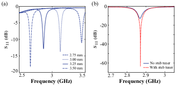
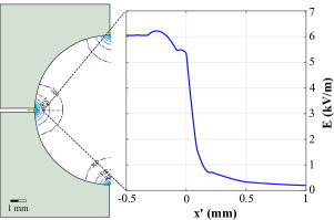
Incident MW power is inductively coupled into the LGR by an exciter antenna, composed of a split ring resonator that is differentially driven by a microstrip balun, as shown in Fig. 1(c). The differential driving mitigates common-mode noise on the two traces, which might otherwise couple to the split-ring resonator. Although the microstrip balun is designed to match the feed-line and the split ring component of the exciter antenna at frequencies near 2.87 GHz, good matching is achieved from 2.5 GHz to 3.5 GHz as well. For drive frequencies between 2.5 and 3.5 GHz, the exciter antenna board couples more than 90 of incident MW power into the LGR, as shown in Fig. 2(a). For a specific fixed frequency, the impedance matching may be further optimized by inserting a stub tuner between the MW source and the exciter antenna board, as shown in Fig. 2(b).
A via shield along a portion of the balun helps reduce interference and cross-talk between traces, controls the trace impedance, and reduces radiative losses along the balun’s -phase delay arm. The exciter antenna is fabricated from 1 oz. copper trace with immersion silver finish on 1.524 mm thick dielectric (Rogers, RO4350B). Although the proximity of the split ring resonator perturbs the field distribution inside the LGR, both simulations and measurements suggest this effect is small and not the dominant inhomogeneity source (see Section IV). For applications intolerant of such perturbations or those requiring maximal diamond optical access, we achieved similar success inductively coupling a small coil of radius to one of the outer loops Koskinen and Metz (1992), where the coil is translated (via mechanical stage) until the desired coupling is achieved. We expect this coupling method to be particularly suitable for laboratory or clinical imaging applications.
IV Loop Gap Resonator Performance
The strength and homogeneity of within the LGR central loop is evaluated employing standard NV techniques, as described in detail in Ref. Pham (2013) and elsewhere Childress (2007); Maze Rios (2010). A 100-cut diamond plate containing NV/cm3 is mounted at the center of the LGR with the 100 crystallographic axis collinear with the LGR axis. A rare earth magnet creates a static magnetic bias field , which shifts the energies of the ground-state Zeeman sublevels. The energy shifts are given to first order by Taylor et al. (2008)
| (5) |
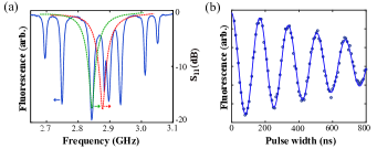
where denotes a unit vector oriented along one of the four diamond crystallographic axes. By judicious choice of , all eight energy levels and associated magnetic dipole transitions can be isolated as shown in Fig. 3(a). The resonator is tuned to excite a single NV transition, yielding Rabi oscillations [Fig. 3(b)]. The data is fit to an exponentially decaying sinusoid in order to extract the Rabi frequency , from which the magnitude of can be calculated as
| (6) |
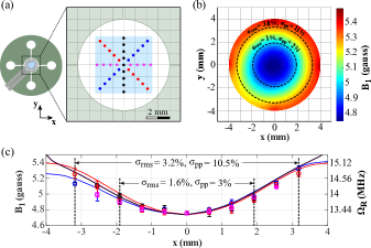
In this geometry, the field is oriented along the [100] crystallographic axis of the diamond, degenerately offset from all four NV axis orientations by half the tetrahedral bond angle . NV Rabi oscillations are driven by the field component transverse to the NV symmetry axis, reducing the Rabi frequency by Sasaki et al. (2016). Accounting for the rotating wave approximation introduces another factor of , resulting in the conversion factor in Eq. 6. To ensure is consistent for all measurements across the LGR central loop [Fig. 4(a)], the confocal excitation volume is held fixed with respect to the -generating permanent magnet, and the diamond and LGR composite device are translated together. We employ a long working distance objective (Mitutoyo 378-803-3, M Plan Apo 10 NA=0.28) to collect the NV fluorescence; the 34 mm working distance is necessary to minimize perturbation of the field by the metal objective housing. Future NV wide-field imaging applications may require ceramic-tipped objectives.
Application of incident MW power 42 dBm yields an axially oriented at the center of the LGR with magnitude 4.7 G. The corresponding Rabi frequency = MHz for NV centers oriented at half the tetrahedral bond angle relative to the LGR axis. Qualitatively, as shown in Fig. 4(c), displays a minimum at the LGR center, increases in magnitude with increasing radial displacement from the center, and is approximately radially symmetric. The best homogeneity is therefore expected at the LGR center.
The field uniformity is quantitatively characterized using both the fractional root-mean-square inhomogeneity and the fractional peak-to-peak variation . The use of both metrics facilitates comparison with alternative existing designs. Over a 32 mm2 circular area axially centered in the LGR central loop, we observe and , as shown in Fig. 4(c). Over a smaller 11 mm2 circular area, we observe and .
The LGR performance is modeled using a commercial finite element MW simulation package (Ansys, HFSS). Simulations include the exciter antenna board, which causes a small perturbation to the otherwise radially symmetric field [Fig. 4(b)]. The simulation predicts 4.8 G at the LGR center with incident MW power dBm. Within a 32 mm2 circular area centered in the LGR central loop, simulations indicate and , whereas in a smaller 11 mm2 circular area, simulations indicate and . These simulation results are in good agreement with the measurements above.
As a three-dimensional cavity resonator, the LGR provides better axial field uniformity than planar-only geometries Le Floch et al. (2016); Kapitanova et al. (2017); Angerer et al. (2016). For example, for a 3.14 mm3 cylindrical volume (1 mm radius disk with 1 mm thickness), simulations yield , and an average of 4.8 G (see Appendix B.3).
V Discussion
The device presented here exhibits further benefits which we now discuss, along with extensions tailored for specific applications. For example, for ubiquitously employed pulsed measurement protocols, a short ring-down time (i.e., field decay time) is necessary for high-fidelity pulse shape control. Although techniques to compensate for long ring-down times are effective Tabuchi et al. (2010); Borneman and Cory (2012); Peshkovsky et al. (2005), shorter native values of are nonetheless generally desired Pfenninger et al. (1995); Rinard and Eaton (2005). The observed loaded quality factor corresponds to a ring-down time of ns (see Appendix B), making the device suitable for standard pulsed protocols Smeltzer, McIntyre, and Childress (2009); Jelezko et al. (2004).
Due to square-root scaling of with incident MW power (), higher power handling can allow for stronger fields. The non-planar resonator design allows for otherwise higher incident MW powers as currents circulate over an extended 2D surface (versus the 1D edge for a planar structure). Further, the metallic LGR thermal mass and thermal conductivity allow efficient heat transfer and sinking, resulting in improved device stability and power handling. Although the latter was not tested, the LGR composite device is expected to allow 100 W for CW and pulsed operation, limited by dielectric breakdown of air in the 260 m capacitive gaps. Should available MW power be constrained, stronger can be achieved by fabricating the LGR from a more electrically conductive material (e.g. silver or copper) at the expense of bandwidth. In such circumstances, the bandwidth can be continuously adjusted above its minimum value by over-coupling the resonator (at the expense of reduced ).
While the presented LGR is 5 mm thick, the fundamental hole-and-slot approach is expected to be feasible for a variety of thicknesses. A thicker device will provide better field uniformity at the expense of optical access. In contrast, for applications requiring MW delivery over a thin planar volume, we expect the LGR can be fabricated via deposition on an appropriate insulating substrate, as discussed in Refs. Twig, Dikarov, and Blank (2013); Twig, Suhovoy, and Blank (2010). We have found semi-insulating silicon carbide Schloss et al. (2018) suitable due to the material’s high thermal conductivity (490 W/(m*K) Haider Protik et al. (2017); Qian, Jiang, and Yang (2017), high Young’s modulus, moderate cost and wide availability in semi-conductor grade wafers. Our simulations suggest the planar LGR approach can offer modest improvements in homogeneity over split ring resonators.
Although the exciter antenna (see Section III) facilitates a compact, vibration-resistant, and portable device, this component introduces non-idealities in both field uniformity and optical access. As similar scattering parameters are obtained by inductively coupling a small coil to one of the LGR outer loops, this latter solution may find favor for applications requiring maximal optical access and, furthermore, requires no PCB fabrication.
In this work, we demonstrated a broadband tunable LGR allowing appplication of strong homogeneous MW fields to an NV ensemble. The LGR demonstrates a dramatic improvement over prior MW delivery mechanisms, both improving on and spatially extending MW field homogeneities. We expect the device to be useful for bulk sensing Acosta et al. (2009); Wolf et al. (2015); Clevenson et al. (2015); Chatzidrosos et al. (2017); Barry et al. (2016) and particularly imaging applications Karaveli et al. (2016); Glenn et al. (2015); Barry et al. (2016); Le Sage et al. (2013); Wu et al. (2016); Fu et al. (2014); Glenn et al. (2017), due to the optical access allowed by the LGR composite device both above and below the diamond.
VI Acknowledgments
The authors would like to thank P. Hemmer, M. Newton, C. McNally, and S. Alsid for helpful discussions, and G. Sandy for resonator design simulations. E. Eisenach was supported by the National Science Foundation (NSF) through the NSF Graduate Research Fellowships Program. Any opinions, findings, conclusions, or recommendations expressed in this material are those of the author(s) and do not necessarily reflect the views of the U.S. Government.
Appendix A Appendix A
A.1 The NV Center in Magnetometry
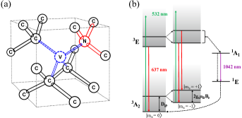
The negatively-charged NV color center (NV-) is a deep band gap impurity within the diamond crystal lattice [Fig. A.1(a)]. The point defect’s symmetry results in a 3A2 spin-triplet ground state and a 3E spin-triplet excited state, separated by a zero phonon line (ZPL) of 637 nm Maze et al. (2011). Spin-spin interactions give rise to a zero-field splitting in the ground-state spin triplet, shifting the states with respect to the state by Dgs 2.87 GHz [Fig. A.1(b)]. In the presence of a static magnetic field , the sublevels experience Zeeman splitting proportional to the projection of the magnetic field along the NV symmetry axis. Above-band optical excitation (typically performed with a 532-nm laser) results in phononic relaxation of the NV spin within the 3E excited state, followed by fluorescent emission in a broad band. While these optical transitions are generally spin-preserving, an alternate decay path through a pair of metastable singlet states (1A1 and 1E) results preferential relaxation from the excited states to the ground state that is non-radiative in the typical nm fluorescence band. This behavior under optical excitation has two major consequences: (1) an optical means of polarizing the NV spin, and (2) optical detection via spin-state-dependent fluorescence intensity.
Measurement of the NV electron spin resonance (ESR) spectrum can be performed by sweeping the carrier frequency of the MW drive field and monitoring NV fluorescence in the visible band. Generally, the continuous optical excitation pumps the NV spin population into the more fluorescent state; however, when the carrier frequency is resonant with an NV spin transition, the NV spin population is cycled into an state, causing decreased fluorescence intensity, which appears as a dip in the ESR spectrum Jensen, Kehayias, and Budker (2017); Rondin et al. (2014). Since the NV symmetry axis may be aligned along one of four possible crystal-defined orientations—each orientation being equally thermodynamically likely in low strain diamond—the ESR spectrum can contain up to eight distinct non-degenerate NV resonances, which probe different field components. The different orientations act as basis vectors, which collectively span the space and allow the total vector field to be reconstructed Jensen, Kehayias, and Budker (2017).
Appendix B Appendix B
B.1 Cavity Ring-down Time
The cavity ring down time of the field is Pfenninger et al. (1995); Rinard and Eaton (2005)
| (B.1) |
At critical coupling , yielding ns.
B.2 Electric Field Simulation
Ideally, the electric fields of the TE01 cavity mode are completely confined within the LGR capacitive gaps, ensuring that remains constant when differently-sized diamonds are placed within the central loop. In practice, fringing electric fields from the capacitive gaps extend partially into the LGR’s central loop as shown in Fig. B.1. However, at distances 1 mm from the capacitive gaps, the electric field magnitude is decreased by from the peak field inside the capacitive gap. Consequently, insertion of a diamond (with at 3 GHz Ibarra et al. (1997)) beyond this region has little if any effect on the LGR resonant frequency .
B.3 Axial Field Uniformity
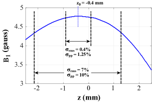
Figure B.2 plots the simulated magnitude of along the LGR’s symmetry axis, illustrating the improved axial field uniformity possible with three-dimensional cavity resonators Le Floch et al. (2016); Kapitanova et al. (2017); Angerer et al. (2016), compared to that of planar-only geometries. The presence of the split ring resonator at mm perturbs inside the LGR, shifting the point of maximal down by 0.4 mm, away from the split ring resonator. Within a cylindrical volume of 3.14 mm3 (1 mm radius and 1 mm thickness), centered around the point of maximal , the simulation predicts and . For a larger cylindrical volume of 12.6 mm3 (2 mm radius and 1 mm thickness), the simulation predicts and . These dimensions are comparable to those of commercially available single-crystal diamonds.
B.4 Smaller Cavity Measurement
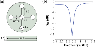
To achieve stronger MW driving, we also designed and fabricated smaller LGR with central loop radius mm and outer loops of radius = 2.45 mm, as shown in Fig. B.3(a). The naked air-gapped LGR cavity exhibits GHz, similar to the larger LGR design described in the main text. Employing the same exciter antenna from Section III, we measure = 5.8 G at the center of the smaller LGR device. Figure B.3(b) depicts for the composite device; the measured 3dB bandwidth MHz corresponds to a loaded quality factor , and an associated ring-down time of 2.8 ns.
References
- Gaebel et al. (2006) T. Gaebel, M. Domhan, I. Popa, C. Wittmann, P. Neumann, F. Jelezko, J. R. Rabeau, N. Stavrias, A. D. Greentree, S. Prawer, J. Meijer, J. Twamley, P. R. Hemmer, and J. Wrachtrup, Nature Physics 2, 408 (2006), quant-ph/0605038 .
- Dutt et al. (2007) M. V. G. Dutt, L. Childress, L. Jiang, E. Togan, J. Maze, F. Jelezko, A. S. Zibrov, P. R. Hemmer, and M. D. Lukin, Science 316 (2007), 10.1126/science.1139831.
- Waldherr et al. (2011) G. Waldherr, P. Neumann, S. F. Huelga, F. Jelezko, and J. Wrachtrup, Physical Review Letters 107, 090401 (2011).
- Hensen et al. (2016) B. Hensen, N. Kalb, M. S. Blok, A. E. Dréau, A. Reiserer, R. F. L. Vermeulen, R. N. Schouten, M. Markham, D. J. Twitchen, K. Goodenough, D. Elkouss, S. Wehner, T. H. Taminiau, and R. Hanson, Scientific Reports 6, 30289 (2016), arXiv:1603.05705 [quant-ph] .
- Taylor et al. (2008) J. M. Taylor, P. Cappellaro, L. Childress, L. Jiang, D. Budker, P. R. Hemmer, A. Yacoby, R. Walsworth, and M. D. Lukin, Nature Physics 4, 810 (2008), arXiv:0805.1367 [cond-mat.mes-hall] .
- Dolde et al. (2011) F. Dolde, H. Fedder, M. W. Doherty, T. Nöbauer, F. Rempp, G. Balasubramanian, T. Wolf, F. Reinhard, L. C. L. Hollenberg, F. Jelezko, and J. Wrachtrup, Nature Physics 7, 459 (2011), arXiv:1103.3432 [quant-ph] .
- Chen et al. (2017) E. H. Chen, H. A. Clevenson, K. A. Johnson, L. M. Pham, D. R. Englund, P. R. Hemmer, and D. A. Braje, Phys. Rev. A 95, 053417 (2017).
- Devience et al. (2015) S. J. Devience, L. M. Pham, I. Lovchinsky, A. O. Sushkov, N. Bar-Gill, C. Belthangady, F. Casola, M. Corbett, H. Zhang, M. Lukin, H. Park, A. Yacoby, and R. L. Walsworth, Nature Nanotechnology 10, 129 (2015), arXiv:1406.3365 [quant-ph] .
- Kehayias et al. (2017) P. Kehayias, A. Jarmola, N. Mosavian, I. Fescenko, F. M. Benito, A. Laraoui, J. Smits, L. Bougas, D. Budker, A. Neumann, S. R. J. Brueck, and V. M. Acosta, Nature Communications 8, 188 (2017), arXiv:1701.01401 [cond-mat.mes-hall] .
- Bucher et al. (2017) D. B. Bucher, D. R. Glenn, J. Lee, M. D. Lukin, H. Park, and R. L. Walsworth, ArXiv e-prints (2017), arXiv:1705.08887 [quant-ph] .
- Sushkov et al. (2014) A. O. Sushkov, I. Lovchinsky, N. Chisholm, R. L. Walsworth, H. Park, and M. D. Lukin, Physical Review Letters 113, 197601 (2014), arXiv:1410.1355 [quant-ph] .
- Lovchinsky et al. (2016) I. Lovchinsky, A. O. Sushkov, E. Urbach, N. P. de Leon, S. Choi, K. De Greve, R. Evans, R. Gertner, E. Bersin, C. Müller, L. McGuinness, F. Jelezko, R. L. Walsworth, H. Park, and M. D. Lukin, Science 351, 836 (2016).
- Neumann et al. (2013) P. Neumann, I. Jakobi, F. Dolde, C. Burk, R. Reuter, G. Waldherr, J. Honert, T. Wolf, A. Brunner, J. H. Shim, D. Suter, H. Sumiya, J. Isoya, and J. Wrachtrup, Nano Letters 13, 2738 (2013), arXiv:1304.0688 [quant-ph] .
- Kucsko et al. (2013) G. Kucsko, P. C. Maurer, N. Y. Yao, M. Kubo, H. J. Noh, P. K. Lo, H. Park, and M. D. Lukin, Nature Physics 500, 54 (2013), arXiv:1304.1068 [quant-ph] .
- Hodges et al. (2013) J. S. Hodges, N. Y. Yao, D. Maclaurin, C. Rastogi, M. D. Lukin, and D. Englund, Physical Review A 87, 032118 (2013).
- Barry et al. (2016) J. F. Barry, M. J. Turner, J. M. Schloss, D. R. Glenn, Y. Song, M. D. Lukin, H. Park, and R. L. Walsworth, Proceedings of the National Academy of Science 113, 14133 (2016), arXiv:1602.01056 [quant-ph] .
- Laraoui et al. (2015) A. Laraoui, H. Aycock-Rizzo, Y. Gao, X. Lu, E. Riedo, and C. A. Meriles, Nature Communications 6, 8954 (2015), arXiv:1511.06916 [cond-mat.mes-hall] .
- Tetienne et al. (2017) J.-P. Tetienne, N. Dontschuk, D. A. Broadway, A. Stacey, D. A. Simpson, and L. C. L. Hollenberg, Science Advances 3, e1602429 (2017), arXiv:1609.09208 [cond-mat.mes-hall] .
- van Oort, Manson, and Glasbeek (1988) E. van Oort, N. B. Manson, and M. Glasbeek, Journal of Physics C Solid State Physics 21, 4385 (1988).
- Nizovtsev et al. (2003) A. P. Nizovtsev, S. Y. Kilin, F. Jelezko, I. Popa, A. Gruber, and J. Wrachtrup, Physica B Condensed Matter 340, 106 (2003).
- Balasubramanian et al. (2008) G. Balasubramanian, I. Chan, R. Kolesov, M. Al-Hmoud, J. Tisler, C. Shin, C. Kim, A. Wojcik, P. R. Hemmer, A. Krueger, et al., Nature 455, 648 (2008).
- Bar-Gill et al. (2013) N. Bar-Gill, L. M. Pham, A. Jarmola, D. Budker, and R. L. Walsworth, Nature Communications 4, 1743 (2013), arXiv:1211.7094 [quant-ph] .
- Myers, Ariyaratne, and Jayich (2017) B. A. Myers, A. Ariyaratne, and A. C. B. Jayich, Physical Review Letters 118, 197201 (2017), arXiv:1607.02553 [cond-mat.mes-hall] .
- Bauch et al. (2018) E. Bauch, C. A. Hart, J. M. Schloss, M. J. Turner, J. F. Barry, P. Kehayias, S. Singh, and R. L. Walsworth, ArXiv e-prints (2018), arXiv:1801.03793 [quant-ph] .
- Degen (2008) C. L. Degen, Applied Physics Letters 92, 243111 (2008), arXiv:0805.1215 .
- Maletinsky et al. (2012) P. Maletinsky, S. Hong, M. S. Grinolds, B. Hausmann, M. D. Lukin, R. L. Walsworth, M. Loncar, and A. Yacoby, Nature Nanotechnology 7, 320 (2012), arXiv:1108.4437 [cond-mat.mes-hall] .
- Maertz et al. (2010) B. J. Maertz, A. P. Wijnheijmer, G. D. Fuchs, M. E. Nowakowski, and D. D. Awschalom, Applied Physics Letters 96, 092504 (2010), arXiv:0912.1355 [cond-mat.mes-hall] .
- Clevenson et al. (2018) H. Clevenson, L. M. Pham, C. Teale, K. Johnson, D. Englund, and D. Braje, ArXiv e-prints (2018), arXiv:1802.09713 [quant-ph] .
- Schloss et al. (2018) J. M. Schloss, J. F. Barry, M. J. Turner, and R. L. Walsworth, ArXiv e-prints (2018), arXiv:1803.03718 [quant-ph] .
- Wickenbrock et al. (2016) A. Wickenbrock, H. Zheng, L. Bougas, N. Leefer, S. Afach, A. Jarmola, V. M. Acosta, and D. Budker, Applied Physics Letters 109, 053505 (2016), arXiv:1606.03070 [cond-mat.mes-hall] .
- Akhmedzhanov et al. (2017) R. Akhmedzhanov, L. Gushchin, N. Nizov, V. Nizov, D. Sobgayda, I. Zelensky, and P. Hemmer, Physical Review A 96, 013806 (2017).
- Le Sage et al. (2013) D. Le Sage, K. Arai, D. Glenn, S. DeVience, L. Pham, L. Rahn-Lee, M. Lukin, A. Yacoby, A. Komeili, and R. Walsworth, Nature 496, 486 (2013).
- Glenn et al. (2017) D. R. Glenn, R. R. Fu, P. Kehayias, D. Le Sage, E. A. Lima, B. P. Weiss, and R. L. Walsworth, Geochemistry, Geophysics, Geosystems (2017).
- Fu et al. (2014) R. R. Fu, B. P. Weiss, E. A. Lima, R. J. Harrison, X.-N. Bai, S. J. Desch, D. S. Ebel, C. Suavet, H. Wang, D. Glenn, D. Le Sage, T. Kasama, R. L. Walsworth, and A. T. Kuan, Science 346, 1089 (2014), http://www.sciencemag.org/content/346/6213/1089.full.pdf .
- Wolf et al. (2015) T. Wolf, P. Neumann, K. Nakamura, H. Sumiya, T. Ohshima, J. Isoya, and J. Wrachtrup, Physical Review X 5, 041001 (2015), arXiv:1411.6553 [quant-ph] .
- Clevenson et al. (2015) H. Clevenson, M. E. Trusheim, C. Teale, T. Schröder, D. Braje, and D. Englund, Nature Physics 11, 393 (2015), arXiv:1406.5235 [quant-ph] .
- Chipaux et al. (2015) M. Chipaux, A. Tallaire, J. Achard, S. Pezzagna, J. Meijer, V. Jacques, J.-F. Roch, and T. Debuisschert, European Physical Journal D 69, 166 (2015), arXiv:1410.0178 [cond-mat.mes-hall] .
- Andrich et al. (2017) P. Andrich, F. Charles, X. Liu, H. L. Bretscher, J. R. Berman, F. J. Heremans, P. F. Nealey, and D. D. Awschalom, npj Quantum Information 3, 28 (2017).
- Zhang et al. (2016) N. Zhang, C. Zhang, L. Xu, M. Ding, W. Quan, Z. Tang, and H. Yuan, Applied Magnetic Resonance 47, 589 (2016).
- Zhang et al. (2018) C. Zhang, H. Yuan, N. Zhang, L. Xu, J. Zhang, B. Li, and J. Fang, Journal of Physics D: Applied Physics 51, 155102 (2018).
- Mrózek et al. (2015) M. Mrózek, J. Mlynarczyk, D. S. Rudnicki, and W. Gawlik, Applied Physics Letters 107, 013505 (2015), arXiv:1503.04612 [physics.atom-ph] .
- Bayat et al. (2014) K. Bayat, J. Choy, M. Farrokh Baroughi, S. Meesala, and M. Loncar, Nano Letters 14, 1208 (2014).
- Sasaki et al. (2016) K. Sasaki, Y. Monnai, S. Saijo, R. Fujita, H. Watanabe, J. Ishi-Hayase, K. M. Itoh, and E. Abe, Review of Scientific Instruments 87, 053904 (2016).
- Twig, Suhovoy, and Blank (2010) Y. Twig, E. Suhovoy, and A. Blank, Review of Scientific Instruments 81, 104703-104703-11 (2010).
- Horowitz et al. (2012) V. R. Horowitz, B. J. Alemán, D. J. Christle, A. N. Cleland, and D. D. Awschalom, Proceedings of the National Academy of Science 109, 13493 (2012), arXiv:1206.1573 [cond-mat.mtrl-sci] .
- Horsley et al. (2018) A. Horsley, P. Appel, J. Wolters, J. Achard, A. Tallaire, P. Maletinsky, and P. Treutlein, ArXiv e-prints (2018), arXiv:1802.07402 [quant-ph] .
- Simpson et al. (2017) D. A. Simpson, R. G. Ryan, L. T. Hall, E. Panchenko, S. C. Drew, S. Petrou, P. S. Donnelly, P. Mulvaney, and L. C. L. Hollenberg, Nature Communications 8, 458 (2017).
- Rose et al. (2017) B. C. Rose, A. M. Tyryshkin, H. Riemann, N. V. Abrosimov, P. Becker, H.-J. Pohl, M. L. W. Thewalt, K. M. Itoh, and S. A. Lyon, Physical Review X 7, 031002 (2017), arXiv:1702.00504 [quant-ph] .
- Breeze et al. (2017) J. D. Breeze, J. Sathian, E. Salvadori, N. McN. Alford, and C. W. M. Kay, ArXiv e-prints (2017), arXiv:1710.07726 .
- Le Floch et al. (2016) J.-M. Le Floch, N. Delhote, M. Aubourg, V. Madrangeas, D. Cros, S. Castelletto, and M. E. Tobar, Journal of Applied Physics 119, 153901 (2016), arXiv:1604.01516 [quant-ph] .
- Creedon et al. (2015) D. L. Creedon, J.-M. Le Floch, M. Goryachev, W. G. Farr, S. Castelletto, and M. E. Tobar, Physical Review B 91, 140408 (2015), arXiv:1412.4331 [cond-mat.mes-hall] .
- Kapitanova et al. (2017) P. Kapitanova, V. Soshenko, V. Vorobyov, D. Dobrykh, S. Bolshedvorskiih, V. Sorokin, and A. Akimov, in American Institute of Physics Conference Series, American Institute of Physics Conference Series, Vol. 1874 (2017) p. 030017.
- Angerer et al. (2016) A. Angerer, T. Astner, D. Wirtitsch, H. Sumiya, S. Onoda, J. Isoya, S. Putz, and J. Majer, Applied Physics Letters 109, 033508 (2016), arXiv:1605.05554 [quant-ph] .
- Doherty et al. (2013) M. W. Doherty, N. B. Manson, P. Delaney, F. Jelezko, J. Wrachtrup, and L. C. L. Hollenberg, Physics Reports 528, 1 (2013), arXiv:1302.3288 [cond-mat.mtrl-sci] .
- Schirhagl et al. (2014) R. Schirhagl, K. Chang, M. Loretz, and C. L. Degen, Annual Review of Physical Chemistry 65, 83 (2014).
- Davis et al. (2018) H. C. Davis, P. Ramesh, A. Bhatnagar, A. Lee-Gosselin, J. F. Barry, D. R. Glenn, R. L. Walsworth, and M. G. Shapiro, Nature Communications 9, 131 (2018).
- Glenn et al. (2015) D. R. Glenn, K. Lee, H. Park, R. Weissleder, A. Yacoby, M. D. Lukin, H. Lee, R. L. Walsworth, and C. B. Connolly, Nature methods 12, 736 (2015).
- Simpson et al. (2016) D. A. Simpson, J.-P. Tetienne, J. M. McCoey, K. Ganesan, L. T. Hall, S. Petrou, R. E. Scholten, and L. C. L. Hollenberg, Scientific Reports 6, 22797 (2016), arXiv:1508.02135 [cond-mat.mes-hall] .
- Acosta et al. (2009) V. M. Acosta, E. Bauch, M. P. Ledbetter, C. Santori, K.-M. C. Fu, P. E. Barclay, R. G. Beausoleil, H. Linget, J. F. Roch, F. Treussart, S. Chemerisov, W. Gawlik, and D. Budker, Physical Review B 80, 115202 (2009), arXiv:0903.3277 [cond-mat.mtrl-sci] .
- Chatzidrosos et al. (2017) G. Chatzidrosos, A. Wickenbrock, L. Bougas, N. Leefer, T. Wu, K. Jensen, Y. Dumeige, and D. Budker, Phys. Rev. Applied 8, 044019 (2017).
- Wood, Froncisz, and Hyde (1984) R. L. Wood, W. Froncisz, and J. S. Hyde, Journal of Magnetic Resonance 58, 243 (1984).
- Froncisz and Hyde (1982) W. Froncisz and J. S. Hyde, Journal of Magnetic Resonance 47, 515 (1982).
- Froncisz, Oles, and Hyde (1986) W. Froncisz, T. Oles, and J. S. Hyde, Review of Scientific Instruments 57, 1095 (1986).
- Piasecki and Froncisz (1993) W. Piasecki and W. Froncisz, Measurement Science and Technology 4, 1363 (1993).
- W. B. Westphal (1972) A. S. W. B. Westphal, Dielectric Constant and Loss Data (Air Force Materials Laboratory, Air Force Systems Command, 1972).
- Hartnett et al. (2006) J. G. Hartnett, M. E. Tobar, E. N. Ivanov, and J. Krupka, IEEE Transactions on Ultrasonics, Ferroelectrics, and Frequency Control 53, 34 (2006).
- Koskinen and Metz (1992) M. F. Koskinen and K. R. Metz, Journal of Magnetic Resonance 98, 576 (1992).
- Pham (2013) L. M. Pham, Magnetic field sensing with nitrogen-vacancy color centers in diamond, Ph.D. thesis, Harvard University (2013).
- Childress (2007) L. I. Childress, Coherent manipulation of single quantum systems in the solid state, Ph.D. thesis, Harvard University (March 2007).
- Maze Rios (2010) J. Maze Rios, Quantum manipulation of nitrogen-vacancy centers in diamond: From basic properties to applications, Ph.D. thesis, Harvard University (2010).
- Tabuchi et al. (2010) Y. Tabuchi, M. Negoro, K. Takeda, and M. Kitagawa, Journal of Magnetic Resonance 204, 327 (2010).
- Borneman and Cory (2012) T. W. Borneman and D. G. Cory, Journal of Magnetic Resonance 225, 120 (2012), arXiv:1207.1139 [quant-ph] .
- Peshkovsky et al. (2005) A. S. Peshkovsky, J. Forguez, L. Cerioni, and D. J. Pusiol, Journal of Magnetic Resonance 177, 67 (2005).
- Pfenninger et al. (1995) S. Pfenninger, W. Froncisz, J. Forrer, J. Luglio, and J. S. Hyde, Review of Scientific Instruments 66, 4857 (1995).
- Rinard and Eaton (2005) G. A. Rinard and G. R. Eaton, Biomedical EPR, Part B: Methodology, Instrumentation, and Dynamics (Kluwer Academic/Plenum Publishers, 2005) pp. 19–52.
- Smeltzer, McIntyre, and Childress (2009) B. Smeltzer, J. McIntyre, and L. Childress, Physical Review A 80, 050302 (2009), arXiv:0909.3896 [quant-ph] .
- Jelezko et al. (2004) F. Jelezko, T. Gaebel, I. Popa, A. Gruber, and J. Wrachtrup, Physical Review Letters 92, 076401 (2004).
- Twig, Dikarov, and Blank (2013) Y. Twig, E. Dikarov, and A. Blank, Molecular Physics 111, 2674 (2013).
- Haider Protik et al. (2017) N. Haider Protik, A. Katre, L. Lindsay, J. Carrete, N. Mingo, and D. Broido, ArXiv e-prints (2017), arXiv:1705.02634 [cond-mat.mtrl-sci] .
- Qian, Jiang, and Yang (2017) X. Qian, P. Jiang, and R. Yang, ArXiv e-prints (2017), arXiv:1712.00830 [cond-mat.mtrl-sci] .
- Karaveli et al. (2016) S. Karaveli, O. Gaathon, A. Wolcott, R. Sakakibara, O. A. Shemesh, D. S. Peterka, E. S. Boyden, J. S. Owen, R. Yuste, and D. Englund, Proceedings of the National Academy of Science 113, 3938 (2016).
- Wu et al. (2016) Y. Wu, F. Jelezko, M. B. Plenio, and T. Weil, Angewandte Chemie International Edition 55, 6586 (2016).
- Maze et al. (2011) J. R. Maze, A. Gali, E. Togan, Y. Chu, A. Trifonov, E. Kaxiras, and M. D. Lukin, New Journal of Physics 13, 025025 (2011), arXiv:1010.1338 [quant-ph] .
- Jensen, Kehayias, and Budker (2017) K. Jensen, P. Kehayias, and D. Budker, in High Sensitivity Magnetometers (Springer, 2017) pp. 553–576.
- Rondin et al. (2014) L. Rondin, J.-P. Tetienne, T. Hingant, J.-F. Roch, P. Maletinsky, and V. Jacques, Reports on Progress in Physics 77, 056503 (2014), arXiv:1311.5214 [cond-mat.mes-hall] .
- Ibarra et al. (1997) A. Ibarra, M. González, R. Vila, and J. Mollá, Diamond and Related Materials 6, 856 (1997).