email: seymur@unam.bilkent.edu.tr
webpage: http://unam.bilkent.edu.tr/ seymur22affiliationtext: Department of Photonics, Izmir Institute of Technology, 35430 Izmir, Turkey33affiliationtext: Department of Physics, University of Antwerp, Groenenborgerlaan 171, B-2020 Antwerp, Belgium
email: hasan.sahin@uantwerpen.be
webpage: http://cmt.ua.ac.be/hsahin44affiliationtext: Aix Marseille Université, CNRS, PIIM UMR 7345, 13397, Marseille, France
email: guy.lelay@univ-amu.fr55affiliationtext: Max Planck Institute for the Structure and Dynamics of Matter and Center for Free-Electron Laser Science Luruper Chaussee 149, 22761 Hamburg, Germany
email: angel.rubio@mpsd.mpg.de
webpage: http://www.mpsd.mpg.de/113438/theod66affiliationtext: Nano-Bio Spectroscopy Group and ETSF, Dpto. Fisica de Materiales, Universidad del País Vasco, CFM CSIC-UPV/EHU-MPC and DIPC, 20018 San Sebastián, Spain
email: angel.rubio@ehu.es
webpage: http://nano-bio.ehu.es/
Introduction to the physics of Silicene and other 2D materials
Abstract
*Research on silicene shows a fast and steady growth that has increased our tool-box of novel 2D materials with exceptional potential applications in materials science. Especially after the experimental synthesis of silicene on substrates in 2012 it has attracted substantial interest from both theoretical and experimental communities. Every day, new people from various disciplines join this rapidly growing field. The aim of this book is to serve as a fast entry to the field to these newcomers and as a long-living reference to the growing community. To achieve this goal, the book is designed to emphasize the most crucial developments from both theoretical and experimental point of view since the starting of the silicene field back in 1994 with the first theoretical paper proposing the structure of silicene. We provide the general concepts and ideas such that the book is accessible to everybody from graduate students to senior researchers and we refer the reader interested in the detail to the relevant literature. We now start with a brief history of silicene where we highlight, in the chronological order, the important works that shaped our understanding of silicene.
Research on silicene shows a fast and steady growth that has increased our tool-box of novel 2D materials with exceptional potential applications in materials science. Especially after the experimental synthesis of silicene on substrates in 2012 has attracted substantial interest from both theoretical and experimental community. Every day, new people from various disciplines join this rapidly growing field. The aim of this book is to serve as a fast entry to the field these newcomers and as a long-living reference to the growing community. To achieve this goal, the book is designed to emphasize the most crucial developments from both theoretical and experimental points of view since the start of the silicene field with the first theoretical paper proposing the structure of silicene. We provide the general concepts and ideas such that the book is accessible to everybody from graduate students to senior researchers and we refer the reader interested in the details to the relevant literature. In the next paragraphs, we present a brief history of silicene where we highlight, in the chronological order, the important works that shaped our understanding of silicene.
The atomic and electronic structure of the materials that we now call silicene and germanene was investigated for the first time by Takeda and Shiraishi, a decade before graphene was obtained by exfoliation from the parent graphite crystal (Takeda1). Using density functional theory (DFT) (Hohenberg1), they have shown that it is energetically favorable for silicene and germanene to become buckled instead of staying planar, as carbon atoms do in the case of graphene. The band structure of silicene was also reported but there was no emphasis on the linear crossing at the Fermi level, namely the Dirac cone. This visionary paper was ignored for almost a decade for two main reasons. First, there was a common belief that these two-dimensional (2D) materials cannot exist in nature (Peierls1; Landau1; Mermin1). Second, it was hard to believe that silicon could acquire an sp2-like hybridization because it always preferred sp3 hybridization (Fagan1).
In 2004, a monolayer of carbon atoms named graphene was isolated from graphite, the layered bulk allotrope of carbon (Novoselov1). This left no doubt about the stability of 2D materials. However, later it was discovered that graphene possesses long-wavelength mechanical oscillations (Meyer1) which are the manifestation of the fact that pure 2D crystals are indeed thermodynamically unstable (Peierls1; Landau1; Mermin1). Graphite was not the only layered material. The monolayer counterparts of other layered materials like hexagonal boron nitride, metal dichalcogenides and metal oxides were also peeled off or synthesized and studied in detail. The layers of these materials are formed by strong covalent bonds while they are kept together by weak van der Walls interactions. The isolation of these layers has opened a possibility of combining these layers in a desired order to create the so-called van der Walls heterostructures that can be engineered to have novel properties (Geim1; Gao1).
Besides being a stable 2D material with impressive mechanical properties (which is also true for the BN monolayer) like having 1.0 terapascal Young’s modulus while being extremely flexible (Lee1), graphene also attracted huge interest due to the linearly crossing bands at the Fermi level that allow its electrons to behave as if they have no mass (Novoselov2). The rise of graphene triggered interest in other possible group IV 2D materials like silicene, germanene and stanene (also written stannene, but rarely, from stannum in Latin, or sometimes called tinene) that would have similar electronic structures. However, they lack a layered parent bulk counterpart like graphite. Synthesis of these 2D materials that lacked bulk counterpart has required a more bottom-up approach, like growing them epitaxially on top of a substrate.
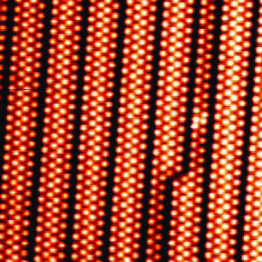
In 2005, silicene (the 2D allotrope of silicon) started to appear in several theoretical and experimental studies. Self-aligned one dimensional (1D) structures of silicon (see Fig. 1) were synthesized on Ag(110) surface (Leandri1). Guy Le Lay, gave the kick to this study by noticing novel quantized states in the region of silver during the angle-resolved photoemission spectroscopy (ARPES) measurements at the Elettra synchrotron radiation source in Trieste, Italy, and inferred the presence of 1D objects prior to their observation in STM imaging. He took inspiration from his earlier work of the reverse system in which Ag was deposited onto silicon surfaces (Lelay1). The same year, Durgun et al. investigated Si nanotubes which were based on the buckled geometry of silicene reported by Takeda and Shiraishi (Durgun1).
In 2007, the planar structure of silicene was investigated using tight-binding Hamiltonians (Guzman1). In this study, it was emphasized that, similar to graphene, the planar structure of silicene would also exhibit linearly crossing bands at the Fermi level. The name ”silicene” was used for the first time in this study. In 2009, Lebégue and Eriksson investigated the electronic properties of several 2D materials including planar structures of silicene and germanene using first-principles DFT calculations (Lebegue1). Similar to the tight binding results mentioned above, their calculations showed that planar silicene had linear bands crossing at the Fermi level. However, planar germanene was found to be a poor metal since the conduction band was partially filled around the -point which shifted the Fermi level below the linear crossing at the -point. This study revived interest in group IV 2D materials beyond graphene but it was unfortunate that the authors adopted the planar structure of silicene and germanene which was shown to be energetically less favorable compared to the buckled one (Takeda1).
In the meantime, after waiting almost a year in the review process, Cahangirov et al. reported a study that answered the question of whether silicon could adopt an -like hybridization to make a stable free-standing 2D structure (Cahangirov1). They have calculated phonon dispersions for both planar and buckled silicene. Planar silicene clearly had imaginary frequencies indicating structural instability, while all phonon modes were positive for the buckled silicene. This meant that buckled silicene had restoring forces to any possible deformation while planar silicene was unstable. They have also emphasized that although buckling was lowering the symmetry of the system, the remaining hexagonal symmetry of the lattice was enough to preserve the linearly crossing bands at the Fermi level. Furthermore, they have shown that similar to their graphene counterparts, armchair silicene nanoribbons displayed the family behavior in the band gap variation with respect to their widths (Cahangirov2). This work boosted many theoretical and experimental investigations on silicene and other 2D materials beyond graphene (Sahin1; Xu2).
On the experimental side, Le Lay et al. continued to study deposition of silicon onto Ag substrates (DePadova1; DePadova2; Kara1; LeLay2). Now their work was clearly inspired by the theoretically predicted stability of silicon structures with -like hybridization and their promising electronic properties. They have also discovered that what they thought to be silicon nanowires were in fact silicene nanoribbons epitaxially grown on Ag(110) surface. Using DFT calculations they were able to reveal the detailed atomic structure of these silicene nanoribbons. Their work continued to build up the idea of a possible formation of monolayer silicene on Ag substrates (Aufray1; DePadova3). ARPES measurements that they performed along the silicene nanoribbons showed linear bands in the vicinity of the Brillouin zone boundary (DePadova3). These linear bands were interpreted as -states of zigzag silicene nanoribbons (DePadova4).
A gold rush started to synthesize 2D silicene. In 2010, ignoring Guy Le Lay’s reservations, some of his former co-workers in Marseille published a letter on the “epitaxial growth of a silicene sheet” on a Ag(111) substrate. This letter was based solely on STM topographs with a highly perfect, nearly flat honeycomb appearance but incredibly short lattice parameter, without a single defect on areas of several hundred nm2! This letter has been a nuisance, creating continuing confusion, although the graphene-like honeycomb appearance was proved to be just an illusion: a mere mirage originating from a contrast reversal in STM imaging of a bare Ag(111) surface (Lelay3). All this perfectly illustrated the famous quote of Luigi Galvani: “for it is easy in experimentation to be deceived, and to think one has seen and discovered what one has desired to see and discover”.
Research on 2D materials received another boost in 2010 after the Nobel Prize in Physics was awarded to Geim and Novoselov for their work on graphene. Silicene acted as a role model for the possibility of other 2D materials beyond graphene. While synthesis of silicene was still expected, theoretical works on silicene continued to progress. Several works investigated the atomic and electronic properties of fully hydrogenated silicene, named silicane (Houssa1; Garcia1; Osborn1). The carbon counterpart, named graphane, had been already synthesized (Elias1) and studied theoretically (Sofo1).
On the other hand, differences between silicene and graphene started to attract some interest. One such difference was originating from the lowered symmetry in silicene due to buckling. Using ab initio calculations, it has been shown that it is possible to tune the band gap of silicene and germanene by applying an electric field in perpendicular direction to the sheets (Ni1; Drummond1). They concluded that this property could be used to build field effect transistors that can operate at room temperature. Another important difference between graphene and silicene is the strength of the spin-orbit coupling. In the case of graphene, the spin-orbit coupling is so weak that the quantum spin Hall effect (QSHE) can only occur at unrealistically low temperatures (Kane1; Yao1). Silicene, on the other hand, was shown to preserve its topologically nontrivial electronic structure despite buckling and to be able to host the QSHE up to 18 K, thanks to the larger spin-orbit coupling in silicon atoms (Liu1; Liu2). In the case of germanene, the QSHE could occur at even higher temperatures up to 277 K and this grows even further for stanene, the tin based analogue, another stable 2D material of the same family that has been synthesized much recently (Zhu1).
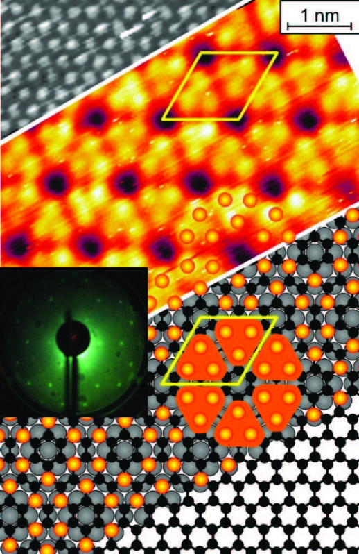
In 2012, the first compelling experimental evidence for the existence of silicene was reported (Vogt1). In this study, they deposited silicon on top of an Ag(111) substrate instead of Ag(110). As a result, a monolayer of silicene with 33 reconstruction was formed, although not directly imaged. The 33 supercell of silicene was perfectly matched with the 44 supercell of the Ag(111) surface. Looking from a distance, the STM image consisted of bright spots arranged in a honeycomb lattice, but, zooming in, it was clear that actually each bright spot was formed by three protruding Si atoms making up the so called “flower pattern”, i.e., a 33 reconstructed silicene cell, as shown in Fig. 2. Having in mind an underlying, hidden, silicene honeycomb structure, Vogt et al. were able reproduce the experimentally observed STM pattern by geometry optimization using DFT calculations. It turns out, as will be seen in more details below, that silicene, on all templates used for growth until now, is always reconstructed: the 11 primitive cell has not yet been observed. The reason is that the first silicene layer conforms to the substrate by changing its lattice parameter and buckling with respect to free standing silicene to find commensurate epitaxial structures. Furthermore, Vogt et al. did ARPES measurements in which they have detected linear surface bands (i.e. non-dispersing with the perpendicular component of the wave vector) starting at 0.3 eV below the Fermi level and extending down to -3 eV with a Fermi velocity of 1.3106 m/s when silicene was present on the surface. No such state was detected on the bare Ag(111) surface in the absence of silicene on top.
Later in the very same year, two more groups reported the experimental realization of silicene using either Ag(111) surface (Feng1) or ZrB2(0001) surface (Fleurence1) as a substrate. Besides the aforementioned 33 reconstructed superstructure, Feng et al. reported other phases that would emerge when the experimental conditions were varied. In particular, a reconstructed silicene structure with a lattice constant of 0.64 nm was observed. This value is 5 lower than the number that one would get by multiplying the 11 unitcell lattice constant by . The STM image of this structure had bright spots arranged in a honeycomb lattice with periodicity. Further deposition of silicon resulted in a second layer of reconstructed silicene grown on top of the first one. This was interpreted as an evidence that structure was intrinsic to silicene and was not dictated by the interaction with the Ag substrate. This claim was further supported by the fact that the shrunk lattice constant of the structure could not be matched by anything on the Ag(111) surface. Although an atomic model for the structure was proposed, it could not explain why the structure was shrinking (Feng1; Chen1). Later, the same group reported STS measurements on the structure (Chen1). They have observed wavelike quasiparticle interference patterns near the boundaries of islands formed by the second silicene layer grown on top of the first one. This suggested the intervalley and intravalley scattering of charge carriers. Furthermore, they have shown that the wavelength of the quasiparticle interference was changing linearly with respect to the applied voltage. This was attributed to a Dirac-like behavior of electrons close to the Fermi level and the Fermi velocity calculated from the slope of this line was reported to be (1.20.1)106m/s which was in agreement with ARPES results for monolayer silicene (Vogt1) and also with those for multilayer silicene nanoribbons (DePadova5) on Ag(110) surfaces. Note that, here the Fermi velocity was obtained from the empty states, at variance with ARPES measuring the filled states.
Upon experimental realization, silicene became a focus of attention and was dubbed “graphene’s silicon cousin” (Nature1; Brumfiel1). It’s exotic electronic structure was explored in a further detail (Ezawa1). In 2013, reconstructed silicene was synthesized on yet another metallic substrate, this time Ir(111) (Meng1). Meanwhile, the nature of the linear bands of silicene on Ag(111) observed in experiments became a hot debate (Lin1; Chen2; Arafune1; Chen3; Wang1; Guo1; Cahangirov3; Gori1). Some part of the community continued to interpret them as Dirac Fermions originating from silicene while others claimed that they were bands of bulk Ag. Each side had reasonable arguments to support their view. The measured Fermi velocity and the range in which the linear bands were extending were to large compared to what was expected from silicene. On the other hand, the linear bands disappeared when silicene was not on top of the Ag substrate. Although this debate is still not fully resolved, there is a growing consensus that the linear bands are originating from the hybridization between silicene and Ag states. Indeed, to put the exotic electronic structure of silicene in use one needs to synthesize it on semiconducting substrates. This seems to remain as a challenge for experimentalists in years to come. Yet, this most probably will be achieved, provided a good template is used. A first indication is the growth of 2D Si nanosheets with local hexagonal structure on a MoS2 surface (Chiappe1).
Meanwhile, De Padova et al. continued studying multilayer silicene (DePadova5; DePadova6; Vogt2). They interpreted the reconstructed structure as the bilayer silicene, since it would usually appear as islands on top of the 33 phase (DePadova6). Using STM they found the surface to be 2 Å above the 33 surface. It was shown that reconstruction was preserved when further layers were grown (Vogt2). The distance between consecutive surfaces was measured to be 3 Å. Interestingly, they have found that the multilayer silicene was metallic.
Although, the reconstruction with shrunk lattice constant and honeycomb STM appearance was observed in many experiments its atomic structure was still a mystery. In 2014, Cahangirov et al. proposed a model that could explain these experimental observations (Cahangirov4). They have shown that formation of the 33 structure on Ag(111) substrate was energetically favorable, but sending more Si atoms on top of this already formed 33 structure would transform it to a structure through formation of dumbbell units. The dumbbell units were formed spontaneously whereby a new-coming Si atom would push one of the silicene atoms down and make the same connections itself on the top (Kaltsas1; Ozcelik1; Marutheeswaran1). It is energetically favorable for dumbbell units to arrange themselves in a honeycomb lattice and to shrink the lattice constant down to 0.64 nm which is exactly what was measured in experiments. Later, it was shown that upon further deposition of Si atoms new layers with reconstruction would form ultimately leading to a bulk structure that they named layered dumbbell silicite (Cahangirov5).
After many experimental advances in silicene research, a new goal was set: to synthesize germanene and stanene. However, it was not possible to synthesize germanene onto Ag(111) because Ge tends to make an ordered Ag2Ge surface alloy. Instead, Dávila et al. deposited germanium on top of the Au(111) surface (Davila1). Although they observed several coexisting phases, a germanene cell matched with a Au(111) one was the best fitting structure to their experimental data and DFT calculations. More work needs to be done to fully characterize the growth and structure of germanene on Au(111) surface. Yet, the progress is very rapid and just at the beginning of 2015, Derivaz et al. managed to synthesize at only 80C a unique, 22 reconstructed, germanene phase on the aluminum (111) surface (Derivaz1). Much recently, stanene was synthesized by molecular beam epitaxy on Bi2Te3(111) substrate (Zhu1). The atomic and electronic characterization of stanene was made by STM and ARPES measurements that showed good agreement with DFT calculations.
In 2015, while this book was still in development, the first silicene field-effect transistor was fabricated and was shown to operate at room temperature (Tao1). To achieve this, they have first synthesized silicene on top of a thin silver film on mica and covered it in situ by a thin alumina layer. Then they delaminated the silver film, flipped the whole structure upside down, and etched some part of the silver until silicene was reached. This resulted in a silicene strip with two Ag pads on top that acted as metal electrodes. This study attracted huge interest and was praised as a “proof of principle” for usage of silicene in electronic devices (Peplow1; Lelay4). Clearly, on the occasion of the 50th anniversary of Moore’s law, it is a hallmark in the quest for 2D materials for electronic applications (Schwierz1).
Acknowledgements
We would like to thank our collaborators including Salim Ciraci, Francois Peeters, Paola De Padova, Patrick Vogt, Maria Carmen Asensio, Maria Davila, Wenhui Duan, Shou-Cheng Zhang, Lede Xian, Peizhe Tang and many others.
Seymur Cahangirov acknowledges financial support from the Marie Curie grant FP7-PEOPLE-2013-IEF project No. 628876 and the Scientific and Technological Research Council of Turkey (TUBITAK) under the project number 115F388. Hasan Sahin is supported by the FWO Pegasus Long Marie Curie Fellowship. Angel Rubio acknowledges financial support from the European Research Council (ERC-2015-AdG-694097), Spanish grant (FIS2013-46159-C3-1-P), Grupos Consolidados (IT578-13), and AFOSR Grant No. FA2386-15-1-0006 AOARD 144088, H2020-NMP-2014 project MOSTOPHOS, GA no. SEP-210187476 and COST Action MP1306 (EUSpec).