revtex4-1Repair the float
Electronic structure of the neutral silicon-vacancy center in diamond
Abstract
The neutrally-charged silicon vacancy in diamond is a promising system for quantum technologies that combines high-efficiency, broadband optical spin polarization with long spin lifetimes ( at ) and up to of optical emission into its zero-phonon line. However, the electronic structure of is poorly understood, making further exploitation difficult. Performing photoluminescence spectroscopy of under uniaxial stress, we find the previous excited electronic structure of a single state is incorrect, and identify instead a coupled system, the lower state of which has forbidden optical emission at zero stress and so efficiently decreases the total emission of the defect: we propose a solution employing finite strain to form the basis of a spin-photon interface. Isotopic enrichment definitively assigns the transition associated with the defect to a local mode of the silicon atom.
Optically-accessible solid state defects are promising candidates for scalable quantum information processing [1; 2]. Diamond is the host crystal for two of the most-studied point defects: the negatively-charged nitrogen vacancy () center [3], and the negatively-charged silicon vacancy () center [4]. has been successful in a broad range of fundamental [5; 6] and applied [7; 8; 9] quantum experiments, with spin-photon [10] and spin-spin [11] entanglement protocols well-established. The superior photonic performance of , with of photonic emission into its zero phonon line (ZPL), has enabled it to make a rapid impact in photonic quantum platforms [12; 13]. However, possesses poor spin coherence lifetimes due to phononic interactions in the ground state (GS) [14], requiring temperatures of to achieve without decoupling [15].
Recent work on , the neutrally-charged silicon vacancy in diamond, has demonstrated that it combines high-efficiency optical spin polarization [16] with long spin lifetimes ( at [17]) and a high degree of coherent emission: the defect potentially possesses the ideal combination of and properties. Exploitation of these promising properties is hindered by poor understanding of the defect’s electronic structure. Electron paramagnetic measurements (EPR) of indicate it has a spin triplet GS and symmetry [18], with the silicon atom residing on-axis in a split-vacancy configuration [Fig 1, inset]. Optically-excited EPR measurements directly relate the spin system to a zero phonon line (ZPL) at [16]: optical absorption experiments and density functional theory (DFT) calculations have assigned the ZPL excited state (ES) to symmetry [19; 20]. Temperature-dependent PL measurements indicate the presence of an optically-inactive state below the luminescent excited state [19].
The advances in exploitation of and have been driven by a concerted effort in the fundamental understanding of the physics of the centers themselves. In this Letter, we employ photoluminescence (PL) spectroscopy to study an ensemble of under applied uniaxial stress, and show that the previous assignment of a single excited state is incorrect. We find that the excited state is , with a state approximately below it. The latter transition is forbidden by symmetry at zero stress and therefore efficiently reduces the emission intensity of unstrained centers at low temperature. However, under finite strain, the proposed electronic structure enables the possibility of resonantly exciting spin-selective optical transitions between the GS and ES. The latter state is shown definitively to participate in the optical spin polarization mechanism of . Finally, we demonstrate that the transition associated with [16], previously hypothesised to be a strain-induced transition [20], is actually a pseudo-local vibrational model (LVM) of primarily involving the silicon atom.
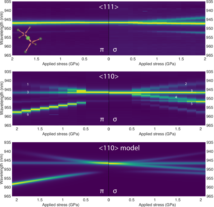
We apply uniaxial stress to a diamond crystal grown by chemical vapour deposition: the crystal was doped with silicon during growth to create and . Uniaxial stress was applied to the sample using a home-built ram driven by pressurized nitrogen gas. PL measurements were collected under excitation at as a function of applied stress in both the \hkl¡111¿ and \hkl¡110¿ directions (see 111See Supplemental Material at http://abc for description of the experimental geometry and apparatus, comparison of spectra with different input polarizations, derivation of the analytical solutions to the coupled stress Hamiltonian, the model parameters used to generate the simulation, and detail on the computation of transition intensities. for detail). We measured spectra for all four combinations of excitation and detection polarization parallel () and perpendicular () to the stress axis. We found that the spectra are essentially invariant to excitation polarization [21]. This is likely due to the excitation mechanism being polarization-insensitive photoionization, as our () excitation laser is above the () photoionization threshold of [22]. We can thus focus on analysing just the spectra for the two detection polarizations (, ) arising from a single excitation polarization ().
The problem of uniaxial stress applied to a trigonal defect in a cubic crystal has been described several times [23; 24; 25], so we summarise the results for transitions to an orbital singlet GS, as found in . In both \hkl¡111¿ and \hkl¡110¿ applied stress, the orientational degeneracy of the defect is lifted into two classes of orientation, classified by the angle between their high-symmetry axis and the uniaxial stress axis. For an orbital singlet-to-singlet () transition, only one transition per orientation is possible: when taking into account both orientation classes, we expect a maximum of two transitions per spectrum. In the orbital singlet-to-doublet () case, two transitions per orientation are possible, leading to a maximum of four transitions per spectrum. \hkl¡111¿ stress does not remove the electronic degeneracy of the orbitals for the orientation parallel to the applied stress, and hence a maximum of three transitions are expected.
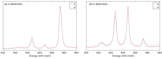
For uniaxial stress applied along the \hkl¡111¿ axis, the ZPL splits into three transitions, two of which are almost degenerate but which possess different emission polarization [Fig. 1]. This is consistent with the case described earlier. Under \hkl¡110¿ uniaxial stress, we identify four distinct components originating at the ZPL, again consistent with an transition. The intensities of the different components varies as a function of applied stress, confirming the presence of electronic degeneracy in the excited state. For both stress directions, we observe additional lower-energy transitions originating at : the transitions gain intensity as a function of stress [Fig. 1]. We measure only two components, indicating the presence of an additional orbital singlet state. At a constant applied stress of , decreasing the temperature increases the intensity of the stress-induced transitions at the expense of the ZPL transitions. Therefore, we conclude the additional state lies below the excited state, rather than above the ground .
In order to construct a model of the excited state behavior, we must establish the origin of the lower-energy state. There are three possible origins: (1) spin-orbit (SO) fine structure arising from the level; (2) Jahn-Teller (JT) vibronic structure arising from the level; and (3) a totally independent level. An SO interaction of () is inconsistent with the magnitude of the SO interaction in ( [4]) and ( [26]) and would yield additional and states (as in ES [27]) and hence we reject this possibility. A JT distortion would place the state above the and hence is inconsistent with experiment. Additionally, the piezospectroscopic parameters describing the singlet and doublet states are significantly different [21], as would be expected if they arise from distinct electronic states [28]. We conclude that the singlet is an additional electronic state and is not derived from the doublet. Experimentally, we find the singlet transitions are polarized in pure for \hkl¡111¿ stress, and pure , for \hkl¡110¿ stress [Fig. 1]: this identifies the level as possessing symmetry in the lowered symmetry of the defect under stress [21].
Building on previous numerical descriptions of a coupled system in trigonal symmetry [28], we construct a full analytical treatment of this problem. For a given SiV sub-ensemble under applied stress, the coupled Hamiltonian is
| (1) |
where , , () describe the response to stress of the () state, and describe coupling between the two states, and is the energy difference between the states at zero stress. , and are functions of the state-dependent piezospectroscopic parameters and are linear in applied stress. The eigenenergies of this Hamiltonian can be parameterised as follows (see [21] for derivation)
| (2) | ||||
where is the stress splitting of the level in the absence of the coupling to the level and is the coupling between the level and the state that also has symmetry under stress. The intensities of the corresponding lines in detection polarization are
| (3) | ||||
where and are intensities of -polarization components of the and transitions (given in [21]), is the angle describing the coupling between the and the substate of the state, and is the partition function.
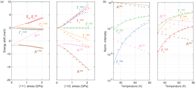
The result of a least-squares fit of this model simultaneously to the experimental \hkl¡110¿ and \hkl¡111¿ spectra as a function of stress is given in Fig. 2(a): piezospectroscopic parameters are detailed in the SI [21]). The output of the model was tested by comparing it to the transition intensities of spectra measured as a function of temperature at a fixed [Fig. 2(b)]. The ordering and behavior of all transitions matches the experiment and hence we accept the coupled model as a suitable description of the excited state.
There are several reasons why the model fit is not perfect. Intrinsic inhomogeneous stress will introduce non-linearities into the line-shifts at low stress; small misalignments or non-uniaxial stress will modify the shift-rates from those taken into account by the model, which will be exacerbated if these effects are different in the two stress directions. Finally, Jahn-Teller interactions in the state, and pseudo-Jahn Teller interactions between the and are not taken into account within the model: high quality absorption data under stress are required to confirm the presence of these interactions, and the low concentration of in the present sample prohibits absorption measurements.
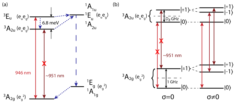
With the excited states’ orbital degeneracy and symmetry under stress confirmed, we now reconcile our observations with the electronic model of . The EPR-active GS arises from the molecular orbital (MO) configuration ( in the hole picture, used henceforth), along with , [20]. The previously-assigned ES arises from [19], in addition to , , , and states. As and are the two lowest-energy one-electron configurations [20], we identify the doubly-degenerate ES observed under stress with the () state.
The requirement of applied stress for observation of the singlet transitions [Fig. 1] indicates that the transitions are forbidden by orbital symmetry but not spin. As the only state arising from the configuration, we assume that the GS of this transition is the EPR-active : the singlet is then restricted by symmetry selection rules to , and . The observed symmetry under stress may be derived from both and in ; however, only the latter is consistent with the electronic model and hence we assign the symmetry (). We identify this state with the state observed in temperature-dependent PL measurements, where the intensity of the ZPL was shown to decrease with decreasing temperature [19].
In addition to the purely electronic transitions discussed above, the PL spectrum of also exhibits a small feature at [16]. In our measurements, we find that the energy shift of the transition under stress is essentially identical and transitions [Fig. 3(a)] [21]. As the line is at lower energy than the associated ZPLs we associate it with a pseudo-LVM in the common GS. This observation is incompatible with previous density functional theory (DFT) calculations suggesting that this transition is a stress-induced electronic transition between a ES and the GS [20].
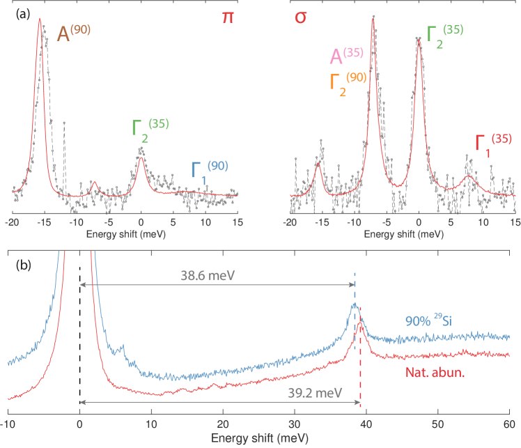
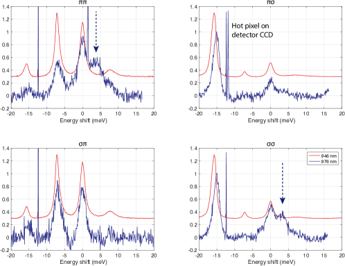
To investigate the participation of Si in the pseudo-LVM, PL measurements of a sample grown with isotopically enriched silicon dopant were performed: we find that the vibration frequency drops from in a natural abundance sample ( \ce^28Si) to in a sample enriched with \ce^29Si [Fig. 3(b)]. Modelling the vibration as a simple harmonic oscillator, the mode frequency under isotopic enrichment is given by , where is the effective mass of the isotopic enrichment, and , are the mode frequency and effective mass in a natural abundance sample, respectively. Applying this model yields , matching the experimental value. This confirms that the LVM is primarily due to oscillation of the Si within the vacancy ‘cage’, and is only weakly coupled to the bulk. Finally, the symmetry of the LVM may be addressed. The similar polarization behavior of the and transitions [Fig 3(a)] indicates an mode. However, only or silicon oscillations participate in pseudo-LVM modes [29]: in both these cases, the overall mode symmetry becomes ungerade and thus vibronic transitions from both and excited states are forbidden by parity. We may reconcile the spectroscopic data with the model only by considering symmetry-lowering distortions. For example, under instantaneous symmetry-lowering distortions from due to (pseudo-)Jahn-Teller distortions in the ES, the mode becomes and the vibronic transition is no longer forbidden. We observe no sharp mode related to the oscillation of the silicon. A similarly complex situation is encountered in , where two pseudo-LVMs have been identified at and [4]. Studies of the latter indicate that its frequency is well-approximated by a simple harmonic oscillator model [30] and essentially involves only the silicon atom, as we find for the mode of . However, experimental measurements assign the mode to symmetry [31; 30] through polarized single-center studies, whereas recent hybrid-DFT calculations assign the mode symmetry and argue that the mode is not an LVM [29]. Further work is required to definitively identify the vibrational states of in both charge states.
With knowledge of the excited state symmetries and behavior under stress, we may re-analyse recent measurements of the spin polarization behavior [16; 17]. The latter measurement identifies significant spin polarization at approximately (Fig. S9 [17]): in light of our new results on the stress-induced optical transition at , we understand that the measurement was performed on a strained ensemble, and interpret its visibility in an absorption spectrum as a direct transition from the ground state to the state [Fig. 4(a)]. As the measurements were completed by reading out spin polarization from the GS, this is direct evidence that the ES is involved in the spin polarization mechanism. At , and hence thermal excitation from to is negligible. The spin polarization mechanism must therefore either involve interactions with both the and states, or via phonon relaxation from the state through [Fig 4(a)]. Information on the relative ordering of the singlet states is required for a full description of the spin polarization mechanism [21].
The thermal interaction of the and states poses a problem for the use of as a photonic resource, as the intensity of the transition decreases with decreasing temperature due to thermal depopulation from into : typically, is required to isolate spin-conserving optical transitions in diamond [32; 33]. For small () stresses applied perpendicular to the symmetry axis, the intensity and frequency of the transition is quadratic in stress: the stress will also remove the spin degeneracy in the spin triplets. Under stress, the spin-conserving optical transitions between GS and ES are no longer forbidden [Fig. 4(b)], and in conjunction with the spin polarization mechanism in may enable spin-dependent optical initialization and readout at low magnetic field. To resolve spin-dependent optical transitions, we require the difference in the zero-field splitting of the GS and ES to be larger than the inhomogeneous linewidth of the transitions themselves. Implementation of this scheme would form the foundation of an spin-photon interface [10]. Future work should include monitoring strained centers in both EPR and resonant PL to determine the effect of strain on the spin-spin interactions in both the orbital singlet states, and measurement of single centers under strain to identify spin-conserving optical transitions.
Acknowledgements.
We thank B. G. Breeze at the University of Warwick Spectroscopy Research Technology Platform for helpful discussion and assistance with experiments. BLG gratefully acknowledges the financial support of the Royal Academy of Engineering. This work is supported by EPSRC Grants No. EP/L015315/1 and EP/M013243/1, and ARC Grants No. DE170100169 and DP140103862.References
- Aharonovich et al. [2016] I. Aharonovich, D. Englund, and M. Toth, Nat. Photonics 10, 631 (2016).
- Rogers et al. [2014a] L. J. Rogers, K. D. Jahnke, T. Teraji, L. Marseglia, C. Müller, B. Naydenov, H. Schauffert, C. Kranz, J. Isoya, L. P. McGuinness, and F. Jelezko, Nat. Commun. 5, 4739 (2014a).
- Doherty et al. [2013] M. W. Doherty, N. B. Manson, P. Delaney, F. Jelezko, J. Wrachtrup, and L. C. L. Hollenberg, Phys. Rep. 528, 1 (2013).
- Rogers et al. [2014b] L. J. Rogers, K. D. Jahnke, M. W. Doherty, A. Dietrich, L. P. McGuinness, C. Müller, T. Teraji, H. Sumiya, J. Isoya, N. B. Manson, and F. Jelezko, Phys. Rev. B 89 (2014b).
- Gaebel et al. [2006] T. Gaebel, M. Domhan, I. Popa, C. Wittmann, P. Neumann, F. Jelezko, J. R. Rabeau, N. Stavrias, A. D. Greentree, S. Prawer, J. Meijer, J. Twamley, P. R. Hemmer, and J. Wrachtrup, Nat. Phys. 2, 408 (2006).
- Hensen et al. [2015] B. Hensen, H. Bernien, A. E. Dréau, A. Reiserer, N. Kalb, M. S. Blok, J. Ruitenberg, R. F. L. Vermeulen, R. N. Schouten, C. Abellán, W. Amaya, V. Pruneri, M. W. Mitchell, M. Markham, D. J. Twitchen, D. Elkouss, S. Wehner, T. H. Taminiau, and R. Hanson, Nature 526, 682 (2015).
- Maletinsky et al. [2012] P. Maletinsky, S. Hong, M. S. Grinolds, B. Hausmann, M. D. Lukin, R. L. Walsworth, M. Loncar, and A. Yacoby, Nat. Nanotechnol. 7, 320 (2012).
- Wang et al. [2015] Y. Wang, F. Dolde, J. Biamonte, R. Babbush, V. Bergholm, S. Yang, I. Jakobi, P. Neumann, A. Aspuru-Guzik, J. D. Whitfield, and J. Wrachtrup, ACS Nano 9, 7769 (2015).
- Rondin et al. [2014] L. Rondin, J.-P. Tetienne, T. Hingant, J.-F. Roch, P. Maletinsky, and V. Jacques, Reports Prog. Phys. 77, 056503 (2014).
- Togan et al. [2010] E. Togan, Y. Chu, A. S. Trifonov, L. Jiang, J. Maze, L. Childress, M. V. G. Dutt, a. S. Sørensen, P. R. Hemmer, A. S. Zibrov, and M. D. Lukin, Nature 466, 730 (2010).
- Bernien et al. [2013] H. Bernien, B. Hensen, W. Pfaff, G. Koolstra, M. S. Blok, L. Robledo, T. H. Taminiau, M. Markham, D. J. Twitchen, L. Childress, and R. Hanson, Nature 497, 86 (2013).
- Sipahigil et al. [2016] A. Sipahigil, R. E. Evans, D. D. Sukachev, M. J. Burek, J. Borregaard, M. K. Bhaskar, C. T. Nguyen, J. L. Pacheco, H. A. Atikian, C. Meuwly, R. M. Camacho, F. Jelezko, E. Bielejec, H. Park, M. Lončar, and M. D. Lukin, Science 354, 847 (2016).
- Sipahigil et al. [2014] A. Sipahigil, K. D. Jahnke, L. J. Rogers, T. Teraji, J. Isoya, A. S. Zibrov, F. Jelezko, and M. D. Lukin, Phys. Rev. Lett. 113, 113602 (2014).
- [14] S. Meesala, Y.-I. Sohn, B. Pingault, L. Shao, H. A. Atikian, J. Holzgrafe, M. Gundogan, C. Stavrakas, A. Sipahigil, C. Chia, M. J. Burek, M. Zhang, J. L. Pacheco, J. Abraham, E. Bielejec, M. D. Lukin, M. Atature, and M. Loncar, arXiv:1801.09833 .
- Sukachev et al. [2017] D. D. Sukachev, A. Sipahigil, C. T. Nguyen, M. K. Bhaskar, R. E. Evans, F. Jelezko, and M. D. Lukin, Phys. Rev. Lett. 119, 223602 (2017).
- Green et al. [2017] B. L. Green, S. Mottishaw, B. G. Breeze, A. M. Edmonds, U. F. S. D’Haenens-Johansson, M. W. Doherty, S. D. Williams, D. J. Twitchen, and M. E. Newton, Phys. Rev. Lett. 119, 096402 (2017).
- [17] B. C. Rose, D. Huang, Z.-H. Zhang, A. M. Tyryshkin, S. Sangtawesin, S. Srinivasan, L. Loudin, M. L. Markham, A. M. Edmonds, D. J. Twitchen, S. A. Lyon, and N. P. de Leon, arXiv:1706.01555 .
- Edmonds et al. [2008] A. M. Edmonds, M. E. Newton, P. M. Martineau, D. J. Twitchen, and S. D. Williams, Phys. Rev. B 77, 245205 (2008).
- D’Haenens-Johansson et al. [2011] U. F. S. D’Haenens-Johansson, A. Edmonds, B. L. Green, M. E. Newton, G. Davies, P. Martineau, R. Khan, and D. Twitchen, Phys. Rev. B 84, 245208 (2011).
- Gali and Maze [2013] A. Gali and J. R. Maze, Phys. Rev. B 88, 235205 (2013).
- Note [1] See Supplemental Material at http://abc for description of the experimental geometry and apparatus, comparison of spectra with different input polarizations, derivation of the analytical solutions to the coupled stress Hamiltonian, the model parameters used to generate the simulation, and detail on the computation of transition intensities.
- Allers and Collins [1995] L. Allers and A. T. Collins, J. Appl. Phys. 77, 3879 (1995).
- Hughes and Runciman [1967] A. E. Hughes and W. A. Runciman, Proc. Phys. Soc. 90, 827 (1967).
- Davies and Hamer [1976] G. Davies and M. E. R. Hamer, Proc. R. Soc. London Ser. A 348, 285 (1976).
- Rogers et al. [2015] L. J. Rogers, M. W. Doherty, M. S. J. Barson, S. Onoda, T. Ohshima, and N. B. Manson, New J. Phys. 17, 013048 (2015).
- Palyanov et al. [2015] Y. N. Palyanov, I. N. Kupriyanov, Y. M. Borzdov, and N. V. Surovtsev, Sci. Rep. 5, 14789 (2015).
- Delaney et al. [2010] P. Delaney, J. C. Greer, and J. A. Larsson, Nano Lett. 10, 610 (2010).
- Davies [1979] G. Davies, J. Phys. C Solid State Phys. 12, 2551 (1979).
- [29] E. Londero, G. Thiering, A. Gali, and A. Alkauskas, arXiv:1605.02955v2 .
- Dietrich et al. [2014] A. Dietrich, K. D. Jahnke, J. M. Binder, T. Teraji, J. Isoya, L. J. Rogers, and F. Jelezko, New J. Phys. 16, 113019 (2014).
- Rogers et al. [2014c] L. J. Rogers, K. D. Jahnke, M. H. Metsch, A. Sipahigil, J. M. Binder, T. Teraji, H. Sumiya, J. Isoya, M. D. Lukin, P. Hemmer, and F. Jelezko, Phys. Rev. Lett. 113, 263602 (2014c).
- Fu et al. [2009] K. M. C. Fu, C. Santori, P. E. Barclay, L. J. Rogers, N. B. Manson, and R. G. Beausoleil, Phys. Rev. Lett. 103, 256404 (2009).
- [33] L. Nicolas, T. Delord, P. Huillery, E. Neu, and G. Hétet, arXiv:1804.05583 .
Supplemental Material
I Experimental detail
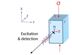
We have measured in a sample grown by chemical vapour deposition. The sample has faces \hkl¡1-10¿, \hkl¡111¿ and \hkl¡11-2¿. Photoluminescence experiments were performed in backscatter geometry i.e. in Porto notation, where and are the excitation and detection vector, respectively [Fig. S1]. As discussed in the main text, we find no dependence of the spectra on the input polarization [Fig. S2], and so all spectra are presented for both detection polarizations only.
Uniaxial stress was applied to the sample using a home-built ram driven by high pressure nitrogen gas and controlled by a Bronkhorst flow controller. The stress cell was mounted into an Oxford Instruments Optistat for low temperature measurements. All measurements were performed using a laser (). The parameters used to generate the model in the main text are given in Table S1.
II Derivation of the stress Hamiltonian solutions
Let the stress Hamiltonian of A and E states in the absence of coupling be
| (S1) |
The Hamiltonian describing the coupling interaction between the states is
| (S2) |
The eigenbasis of the coupling-free is
| (S3) |
Transforming into this basis, the matrix representation of the total Hamiltonian is
| (S4) |
The expressions for , and are defined by the symmetry of the center (), and are given below following [1; 2]:
| (S5) | ||||
Here, the refer to elements of the stress matrix expressed in the crystal axes. is defined as but with , to reflect the different piezospectroscopic response of the doublet and singlet states. Similarly, and are as , with and . is the difference in energy between the doublet and singlet excited states. The reduced matrix elements , , , and have the same form as given by [3].
We now construct the Hamiltonian for each sub-ensemble for each stress direction.
\hkl¡111¿ stress
The angle between the defect symmetry axis and the applied stress axis is denoted . For \hkl¡111¿ stress applied to a trigonal defect, we need only consider two cases: the ‘unique’ orientation with ; and the three equivalent orientations with .
The stress matrix is constructed as , where run over the crystal axes , and is subsequently rotated into each orientation frame. For the representative orientations 1 & 2 [see Table S2] with the substitution , the Hamiltonian parameters are:
Finally, the eigenvalues of the resulting Hamiltonian are as above with and :
\hkl¡110¿ stress
For \hkl¡110¿ applied stress, we need again only consider two cases: the pair of orientations with ; and the pair of orientations with . For the representative orientations 1 & 3 [see Table S2], the Hamiltonian parameters are:
As found in the \hkl¡111¿ case, and .
| 1 | |||
|---|---|---|---|
| 2 | |||
| 3 | |||
| 4 |
III Intensities of stress-split transitions
As discussed above and in the main text, for photoluminescence stress measurements performed with an ionizing input beam, the spectra are essentially invariant to input polarization and therefore the expected intensities therefore reduce to the case encountered in absorption measurements.
The expressions for the intensities given in the main text require the intensities of each transition at zero stress in the experimental geometry. The analytical values have been calculated in several places [3; 4]. However, the sample used in our experiment has \hkl111, \hkl11-2 and \hkl1-10 faces: the standard tables give intensities for \hkl¡110¿ or \hkl¡001¿ readout under \hkl¡1-10¿ stress. In Table S3 we give the zero-stress intensities for both \hkl¡111¿ and \hkl¡110¿ stress, including intensities of transitions when measured with detection polarization under , as found in our experiment.
| Stress | Orientation | Sym. | Energy | |||
| 0 | 1 | |||||
| 0 | ||||||
| 0 | ||||||
| 2 | 0 | |||||
| 0 | ||||||
IV 976 nm transition
As described in the main text, the qualitative behavior of the and transitions is identical. However, a small additional transition appears in certain excitation-detection combinations, namely and [Fig S3]. As no other features of the system are sensitive to input polarization in these measurements, we attribute this additional peak to an unrelated feature.
V Spin polarization mechanism
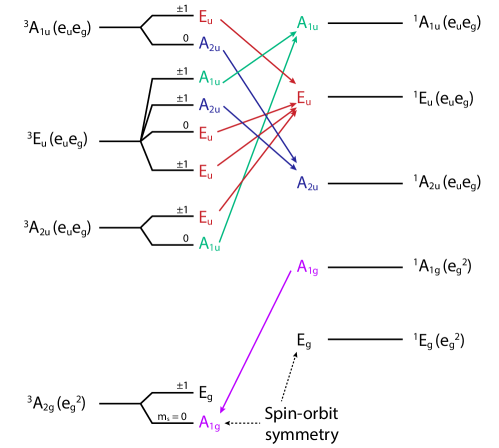
The electronic structure of is complex, with three and six electronic states arising from the first two lowest-energy electronic configurations and , respectively. Considering only symmetric phonons, the first-order intersystem crossings (ISC) from the triplet manifold to the singlet manifold are given in Fig. S4. In this picture, there are no ISCs from the to lower-energy singlet states, suggesting spin polarization should decrease at low temperature, contrary to experiment. Additional information on the relative energy and ordering of the singlets is required for further analysis.
References
- Hughes and Runciman [1967] A. E. Hughes and W. A. Runciman, Proc. Phys. Soc. 90, 827 (1967).
- Davies [1979] G. Davies, J. Phys. C Solid State Phys. 12, 2551 (1979).
- Davies and Hamer [1976] G. Davies and M. E. R. Hamer, Proc. R. Soc. London Ser. A 348, 285 (1976).
- Mohammed et al. [1982] K. Mohammed, G. Davies, and A. T. Collins, J. Phys. C Solid State Phys. 15, 2779 (1982).
- Rogers et al. [2015] L. J. Rogers, M. W. Doherty, M. S. J. Barson, S. Onoda, T. Ohshima, and N. B. Manson, New J. Phys. 17, 013048 (2015).