Laser Annealing for Radiatively Broadened grown by Chemical Vapor Deposition
Abstract
We report on a laser annealing procedure which greatly improves the quality of suspended monolayers of chemical vapor deposition (CVD) grown . Annealing with a green laser locally heats the suspended flake to approximately 600 K, which both removes contaminants and reduces strain gradients. At 4 K, we observe linewidths as narrow as 3.5 meV (1.6nm) full-width at half-max (FWHM) for both photoluminescence (PL) and reflection. Large peak reflectances up to 47% are also observed. These values are comparable to those of the highest quality hexagonal boron nitride (hBN) encapsulated samples. We demonstrate that this laser annealing process can yield highly spatially homogeneous samples, with the length scale of the homogeneity limited primarily by the size of the suspended area. Annealed regions are very stable, exhibiting negligible deterioration over 24 hours at cryogenic temperatures. The annealing method is also very repeatable, with substantial improvements of sample quality on every spot () tested.
pacs:
Valid PACS appear hereI Introduction
Recently, there has been tremendous interest in layered transition metal dichalcogenides (TMDCs). This was sparked by the discovery that the canonical TMDC becomes a direct bandgap semiconductor when isolated in monolayer form Mak et al. (2010); Splendiani et al. (2010). Many of the TMDCs have since been shown to exhibit a strong excitonic feature, showing strong and spectrally narrow PL and reflection. Since then, many other TMDCs have been isolated in monolayer form, exhibiting interesting coherence, spin-valley, and strain properties Jones et al. (2013); Xiao et al. (2012); Mak et al. (2012a); Conley et al. (2013). TMDCs have become a popular testbed for many-body electron physics You et al. (2015); Sidler et al. (2016) and have attracted attention in the quantum optics community due to their potential applicability to exotic exciton-polariton condensates and quantum dot arrays deterministically patterned with electrostatic gating Wang et al. (2018) or engineered strain Palacios-Berraquero et al. (2017).
Mechanical exfoliation Mak et al. (2010); Splendiani et al. (2010) is one of the most popular methods to produce monolayer flakes, and while it is possible to produce very high quality flakes in this manner, the samples tend to be small ( for TMDCs). Flakes produced by mechanical exfoliation are also typically somewhat n-doped, so that electrostatic control is necessary to make the semiconductor neutral Sidler et al. (2016); Mak et al. (2012b).
The highest quality flakes are produced by mechanical exfoliation and subsequent encapsulation in hBN Cadiz et al. (2017); Scuri et al. (2018); Back et al. (2018). Typically, encapsulation leads to even smaller flake sizes and is a time-consuming process. These samples are often annealed in air or inert gas either during or after heterostructure fabrication to reduce contaminants between layers Cadiz et al. (2017). Microscopic spatial inhomogeneity of the exciton resonance energy is ubiquitous in exfoliated and encapsulated TMDC samples. Even the highest quality samples demonstrated to date (as measured by linewidth and peak reflectance) exhibit uncontrolled linewidth-scale spatial variation of the exciton resonance over Scuri et al. (2018), and meV variation over Cadiz et al. (2017). This severely limits the rate of scientific progress in understanding TMDC exciton physics and presents a barrier that must be overcome for practical scaling of TMDC-based optical and electronic devices. The inhomogeneity is due to a combination of strain gradientsMennel et al. (2018), material defects Hong et al. (2015); Wang et al. (2015), electrostatic substrate doping effects Xue et al. (2011) and surface contamination.
Monolayers can also be directly grown on substrates, typically by CVD. This leads to much larger flakes, up to single crystal and continuous wafer-scale polycrystalline Yu et al. (2013); Lee et al. . While many interesting effects and devices have been demonstrated using CVD grown TMDCs, these monolayers are much lower quality Nan et al. (2014) by at least several important metrics (most notably PL and reflection linewidth at low temperature) when compared to mechanically exfoliated flakes. This is despite the fact that defect densities in CVD and exfoliated monolayers are comparable Hong et al. (2015). The lower quality of CVD monolayers is likely due to a combination of adsorbed contaminants that are difficult to remove, and strain gradients from the growth/transfer processes Wood et al. (2015); Amani et al. (2016).
II Results
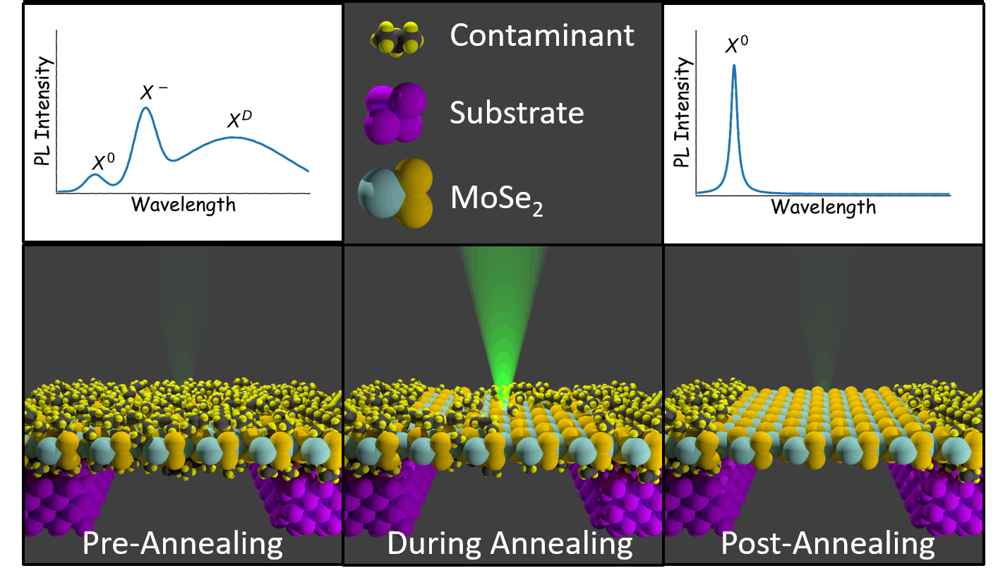

We report on a laser annealing procedure for improving the quality of monolayers of the TMDC to levels comparable with hBN-encapsulated samples. The process can be tuned to yield highly spatially homogeneous samples. It is also repeatable, in the sense that annealing significantly improved sample quality on every spot tested. The annealing process involves heating suspended monolayers of to between 500 and 600 K in high vacuum using an above-bandgap green laser. Note that this is done in a cryostat, so that the nominal substrate temperature is 4 K. Unless otherwise mentioned, all measurements were performed at 4 K and Torr. We hypothesize that this heating effectively removes contaminants and extrinsic dopants adsorbed on the monolayer. The heating in a radially symmetric manner also relaxes the strain pinning at the edge of the suspended layer and the spatial strain gradient is dramatically reduced. A schematic of the annealing process is shown in Fig. 1a.
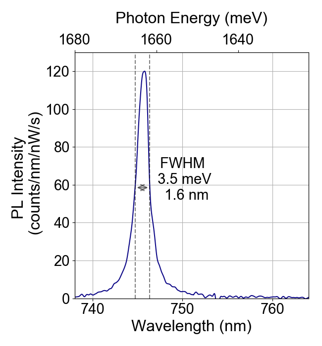
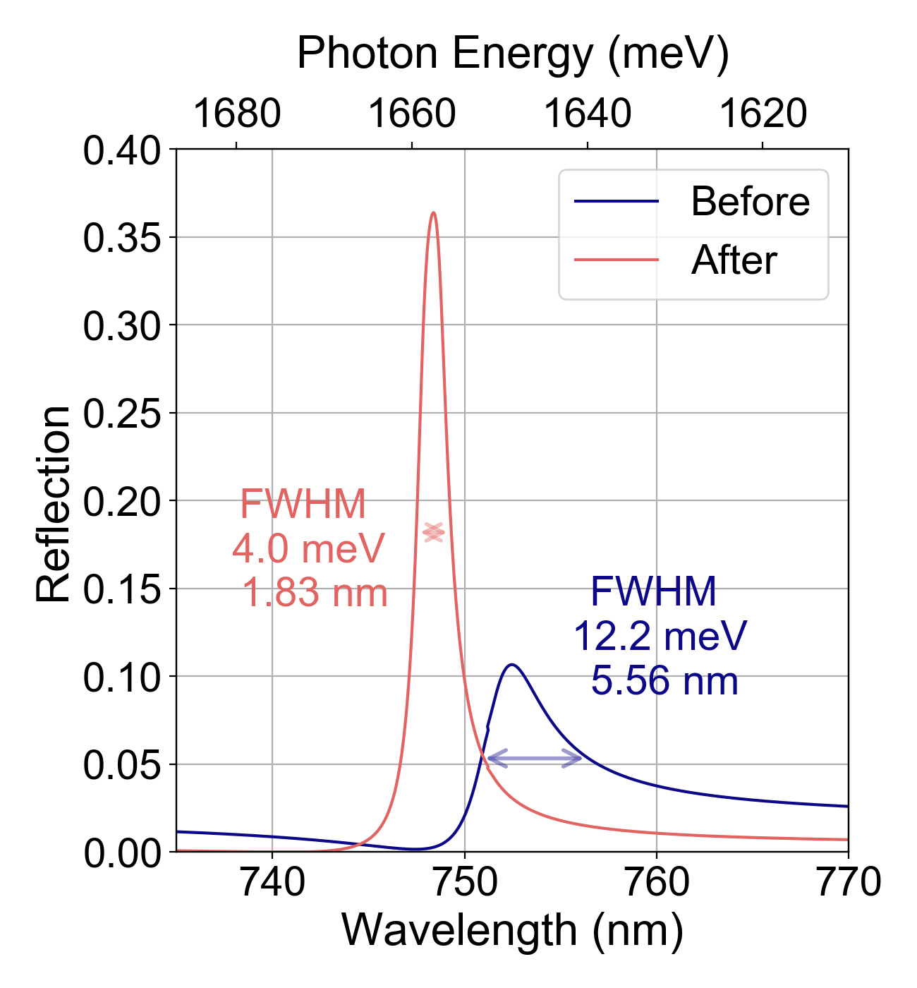
Figs. 1c,1d show some of the narrowest PL and reflection from the annealed monolayers. The PL reflection full-width at half-max (FWHM) are both 3.5 meV. This is comparable to the range of 2.4-4.9 meV, for PL from high quality encapsulated samples from Cadiz et al. (2017). It is worth noting that the dielectric environment for our suspended samples is much different than that for encapsulated samples. Excitons in encapsulated see a larger effective dielectric constant and thus have a smaller binding energy Florian et al. (2018). This higher effective dielectric constant in turn leads to a longer radiative lifetime and smaller exciton radius Robert et al. (2016). Thus, the intrinsic radiative lifetime in suspended layers is smaller than that for encapsulated layers. Therefore, even in a system free of defects, contaminants and strain, at zero temperature (where the exciton is purely radiatively broadened), the linewidth of encapsulated samples would be smaller than that of suspended samples.
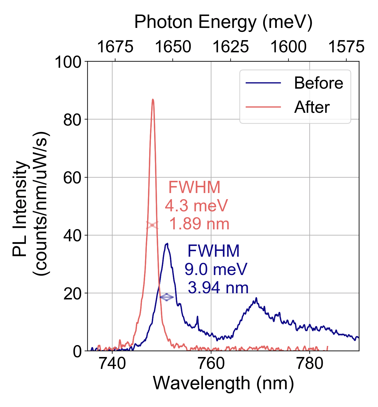
Typical PL and reflection spectra both before and after annealing are shown in Fig 1e. After annealing, the PL shows a drastic reduction in linewidth. The trion PL is also reduced to negligible intensity, indicating that the annealed sample is neutral. We attribute these effects primarily to removal of contaminants from the surface of the sample. It has been shown that water and oxygen are among the primary adsorbents that can cause PL modulation through charge transfer Tongay et al. (2013), and thus it seems likely that the annealing process reduces doping by removing these and other adsorbed molecules. Adsorbed molecules could lead to atomic-scale variations in the dielectric and electrostatic environment seen by the exciton, manifesting as inhomogeneous broadening of the and frequency. The intensity of the emission (often associated with defect emission Tongay et al. (2013)) is also reduced below the noise floor of our measurements. This suggests that is also due to the interaction of excitons with molecules adsorbed on the monolayer.
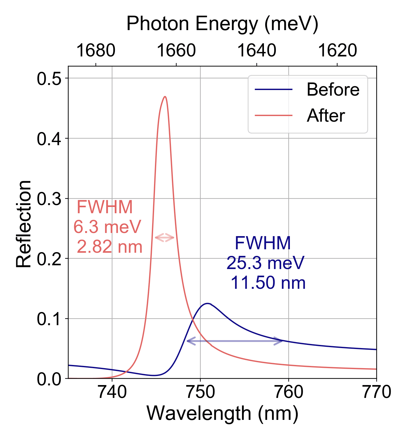
The spectrum with the highest peak reflection of from an annealed spot is shown in 1g. Assuming a simple Lorentzian model for the reflection including dephasing, radiative decay, and non-radiative decay terms, a peak reflection of 47% indicates that the exciton is radiatively broadened. The maximum reflection of the exciton feature is related to the radiative broadening and the total linewidth broadening by Scuri et al. (2018); Back et al. (2018). This leads to a ratio between radiative and all other broadening of . The maximum reflection of 47% observed here thus corresponds to a ratio of 2.2 between radiative broadening and all other broadening and a radiative broadening of 4.3 meV.
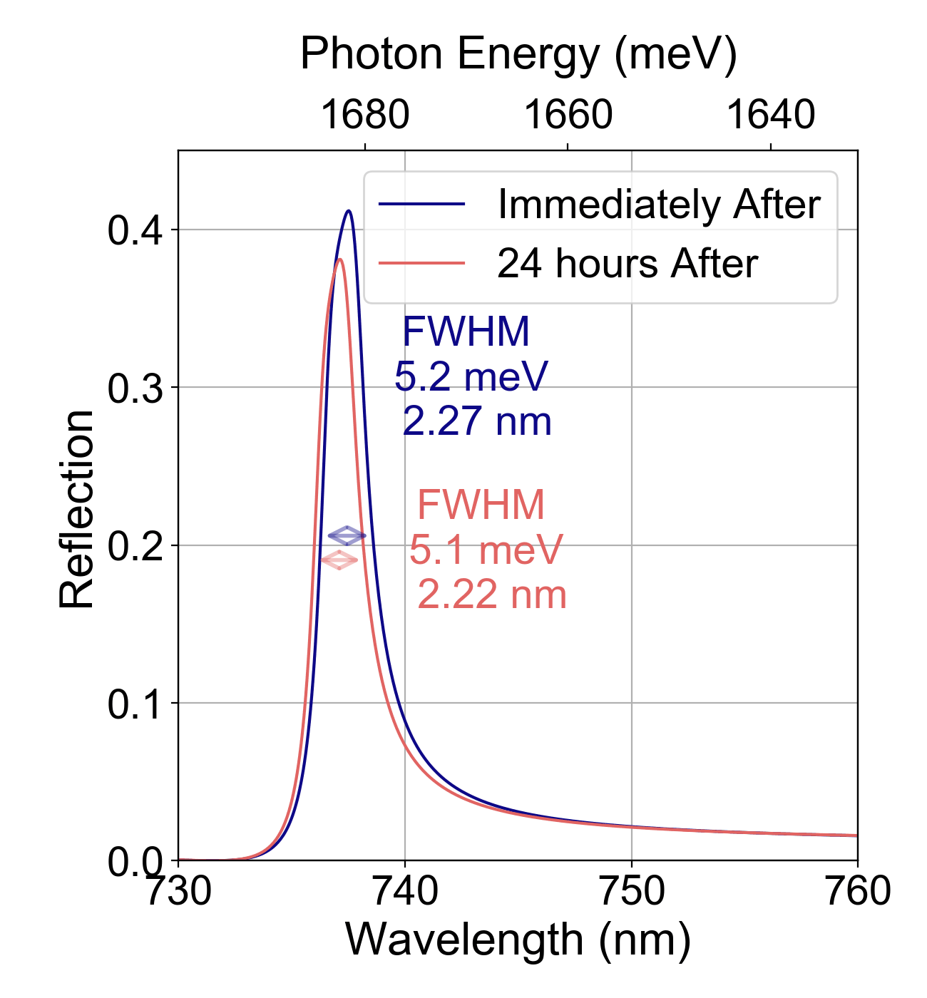
Here we note that after annealing the sample properties were very stable. There were no appreciable changes over 24 hours (the longest time over which we measured), when the samples were kept at high vacuum () and the cryostat was kept at its base temperature of 4 K. An example of the reflection immediately after annealing and 24 hours after annealing is shown in Fig 1h. The reflection changes very little over 24 hours. The small changes that are present may be due to the fact that there is some unavoidable drift in the system, which leads to change in both the coupling efficiency of the collection and the location of the spot on the sample. We expect that the samples would also be stable under high vacuum at room temperature, although we were not able to test this in our system, which relies on cryo-pumping to achieve high vaccum. The flake quality degrades somewhat after warming and leaving at room temperature and 1 Torr for 24 hours, and then cooling back down. For the data in Fig. LABEL:sfig:BeforeAfter, the PL linewidth went from 5.6 meV after annealing to 7.0 meV after the warm-up cycle. Note that since the holes in the substrate are closed, any contaminants removed from the bottom of the suspended film by the annealing are trapped, and may re-adsorb when the entire sample is heated to room temperature. However, these degraded flakes are higher quality than before annealing, and the degradation can be fully reversed by re-annealing. In the case of Fig. LABEL:sfig:BeforeAfter, the linewidth is improved to 5.3 meV after re-annealing. See Fig. LABEL:sfig:BeforeAfter for details.

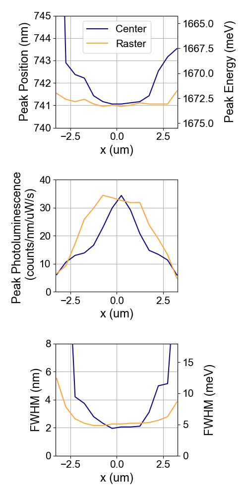
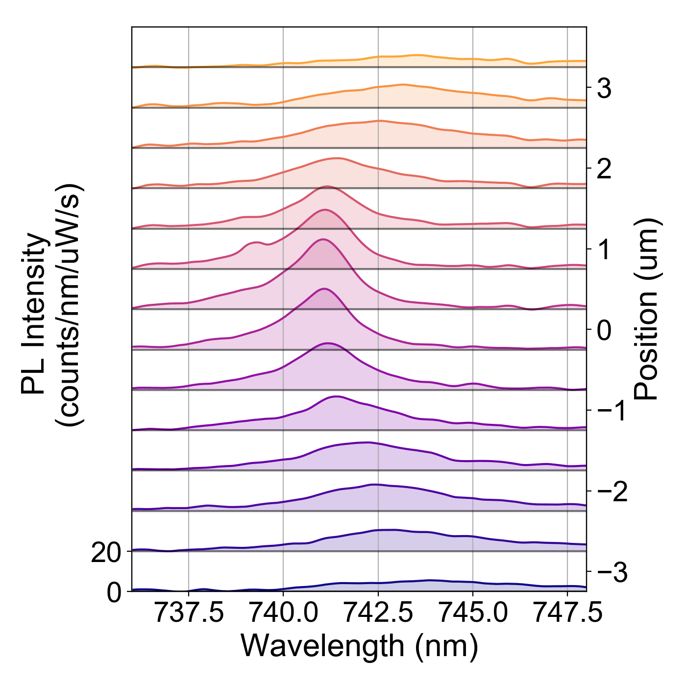
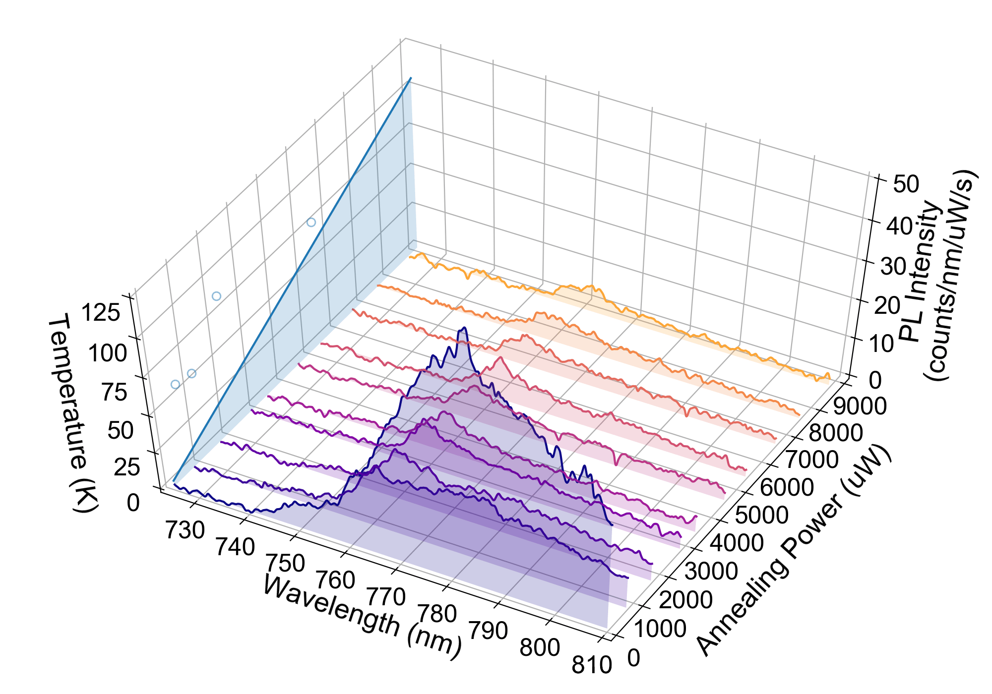
It is possible to improve the spatial homogeneity of the annealed samples by raster scanning the annealing laser over the entire suspended area. This more fully removes contaminants from the entire suspended area, and can also have implications for the spatial strain gradient present in the flake. PL after annealing in the center with a laser spot much smaller than the hole (no raster scan) is shown in 2b. The spectra were taken in a line across a hole with suspended . The extracted peak position, FWHM and amplitude are also shown. It is apparent that both the line position and the quality of the flake, as measured by PL intensity and linewidth, vary substantially across the flake. The quality is much higher in the middle (where the annealing laser was centered) than at the edges. The line position varies parabolically about the center, possibly due to some combination of larger strain gradient and more contaminants near the edges of the suspended area.
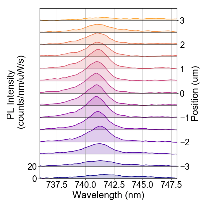
PL after raster scanning the annealing beam over the entire suspended area is shown in Fig. 2c. The spectra were taken across the same as above. In this case, the line position is almost constant over most of the suspended area, changing by less than 1 meV (less than half the linewidth) over . The PL intensity is also much more uniform, with the spatial FWHM being about , as opposed to before. The length scale of the spatial homogeneity in this case appears to be limited by the size of the hole. This is in stark contrast to exfoliated supported flakes, where the line center can shift by more than 10 meV over only a few microns. Even very high quality encapsulated samples can show linewidth-scale variation over Scuri et al. (2018), and meV variation over Cadiz et al. (2017). We note that raster annealing with position-dependent annealing power could further improve homogeneity near the edges of the suspended. For the constant-power anneal performed here, the annealing temperature is higher when the beam is near the center because the center is more thermally isolated from the substrate.

When raster scanning the annealing beam, it is important that the final annealing position of the beam be at or near the center of the hole. This is likely due to strain effects. When the sample is cold, we hypothesize that the flake is essentially pinned on the substrate. However, when supported areas of the flake (especially those near the edge of the hole) are heated during the annealing, the flake can more readily slide across the substrate, changing the strain distribution. When annealing in the center, the areas of the flake at the edge of the hole are equally mobile. This ensures that the strain gradient in the suspended flake is minimized. If the final anneal spot is not centered, the flake could be more mobile on one side of the hole than on another, creating a non-uniform tensile force pulling from the edge of the hole. This would result in a strain gradient in the suspended monolayer. This strain gradient effect based upon the location of the final anneal spot is very repeatable — that is, after a full raster anneal one can alternately anneal near the edge of the sample and then in the middle, and the line position homogeneity changes accordingly. See Fig. LABEL:sfig:RasterAnneal for related plots of the PL homogeneity when the final anneal spot is not in the center, and for the repeatability of this effect.
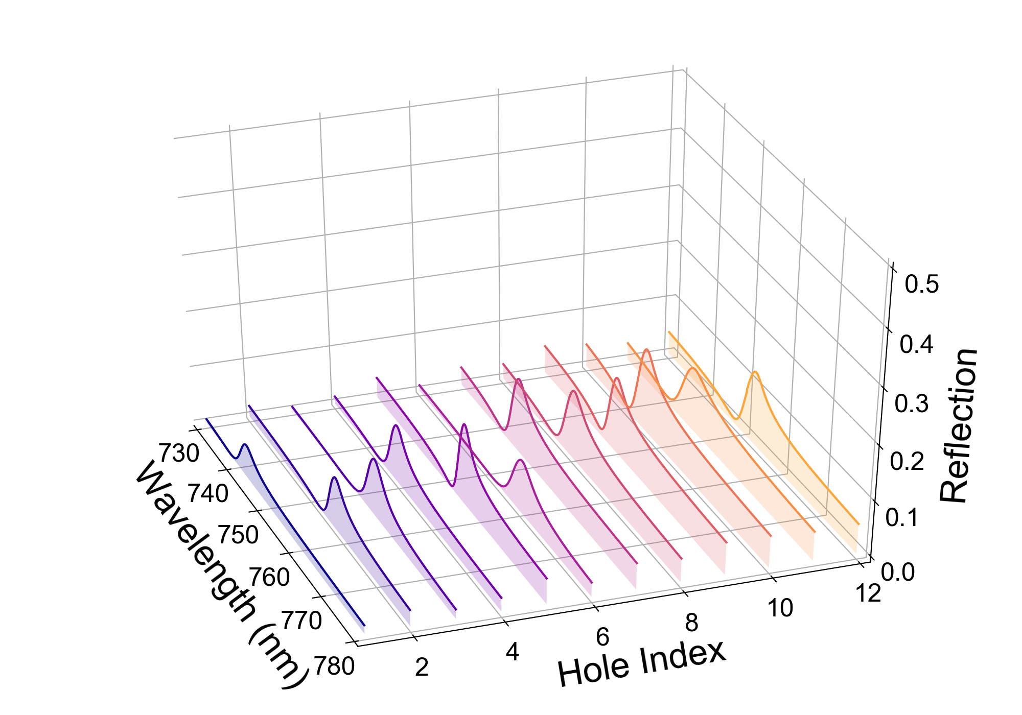
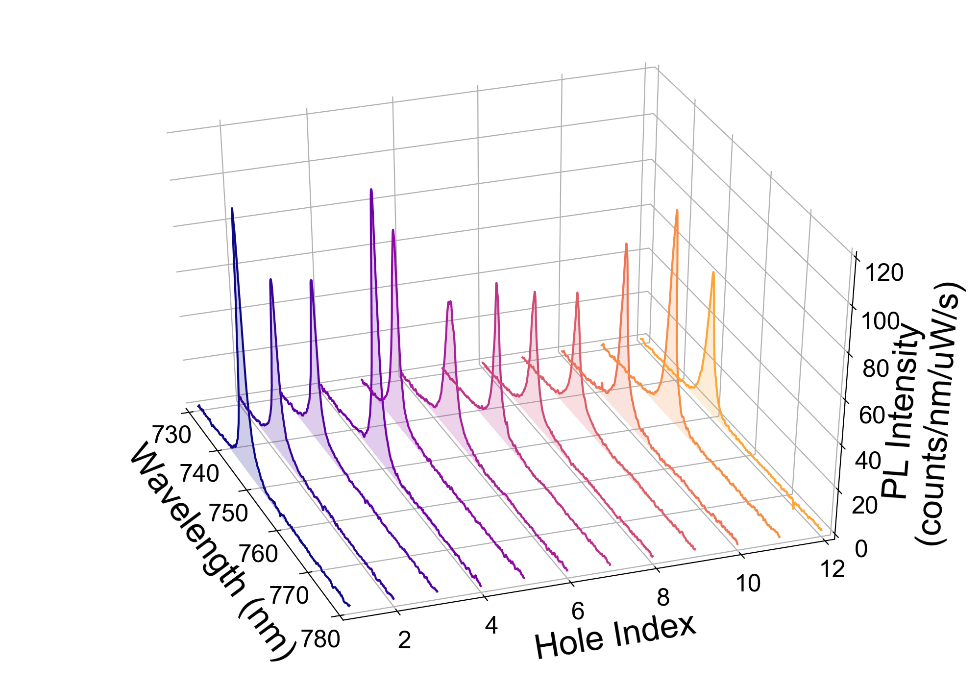
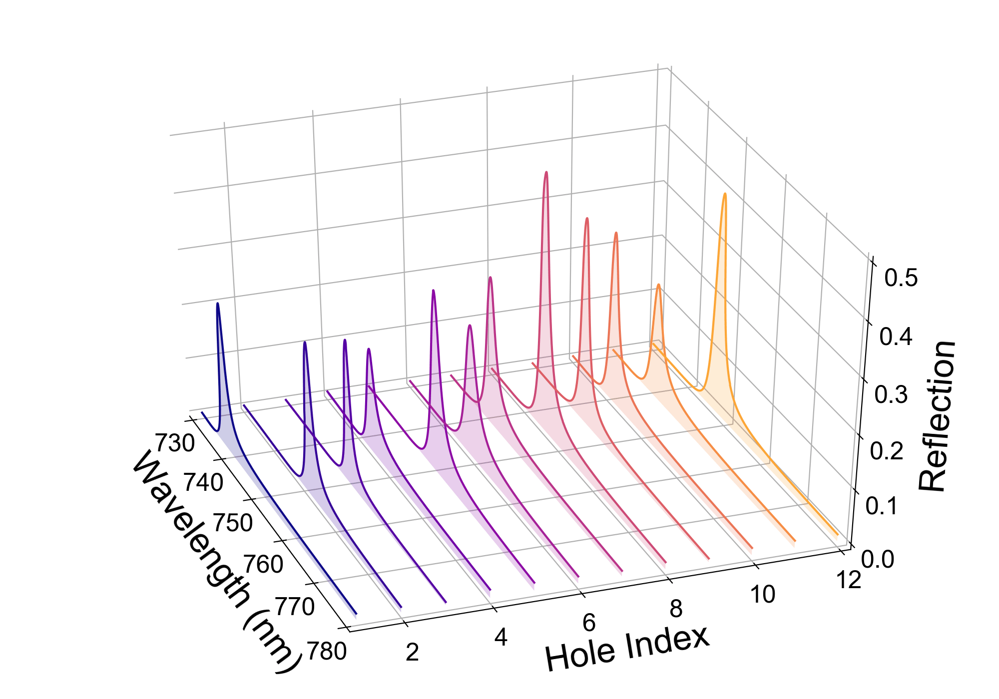
Annealing significantly improved sample quality on every spot investigated (). However, there was variability in line position, linewidth and peak reflection/PL intensity. Fig. 3 shows reflection spectra both before and after annealing at 12 spots, as well as PL before and after for 12 different spots. Note that the holes were not pre-or post-selected in any way, other than to choose holes that did in fact have monolayer suspended . The data collected at each hole was post-selected in that each hole was annealed with successively higher laser power and the qualitatively best spectrum from each hole was selected. There is some variation in the optimal annealing power from hole to hole, which is discussed further below.
Reflection shows a marked change; in some cases the peak reflection increases by as much as and in all cases improves significantly. Before annealing, there is a quite large reflectance from the suspended film, in some cases above 5%. For such a broadband reflection, this is much larger than one would expect from alone Li et al. (2014). We attribute this to a relatively thick layer of hydrocarbon contaminants on the suspended flake. The much lower broadband reflection after annealing indicates the removal of this layer. X-ray-photoelectron spectroscopy (XPS) measurements indicate that there is a hydrocarbon layer as thick as 5 nm on the . See Fig. LABEL:sfig:XPS for more discussion, and XPS data.
In PL, we see that both the and emission are reduced to below the noise floor for all 12 spots. The PL peak intensity increases for almost all spots, and the linewidth decreases by a factor of two for most spots. There is also a consistent blue shift of 10-15 meV after annealing. This is most likely due to a reduction in tensile strain Conley et al. (2013), but could also be related to removing certain contaminants and dopants from the surface, possibly changing the effective dielectric environment seen by the exciton.
Samples exfoliated from bulk were also annealed, and behaved similarly to the CVD samples presented here. See Fig. LABEL:sfig:BeforeAfterSiN for more details.
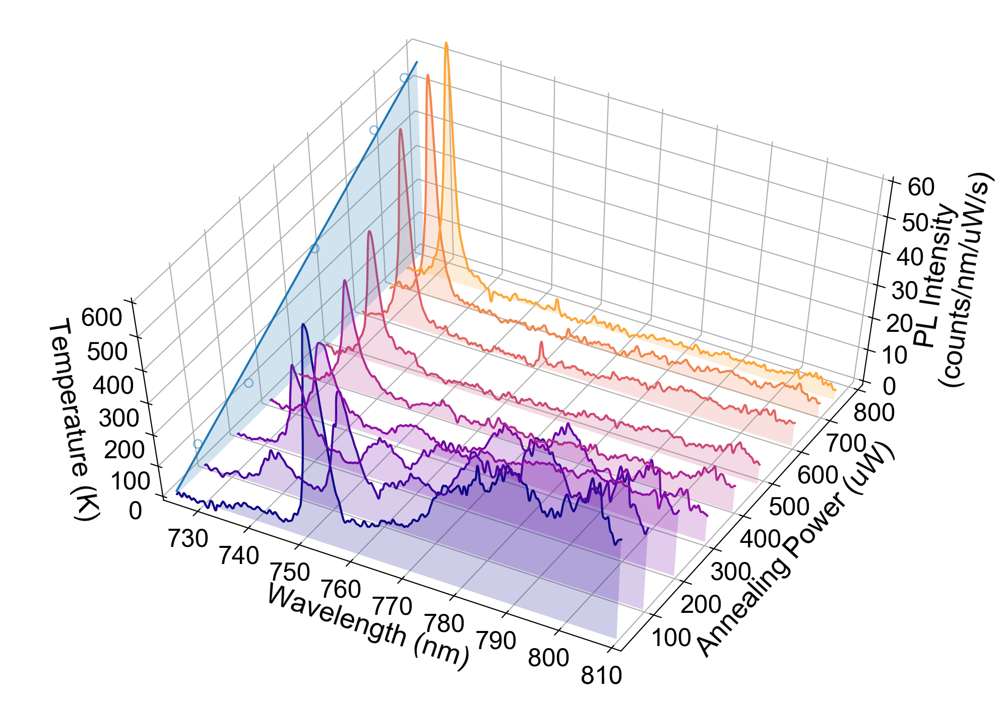
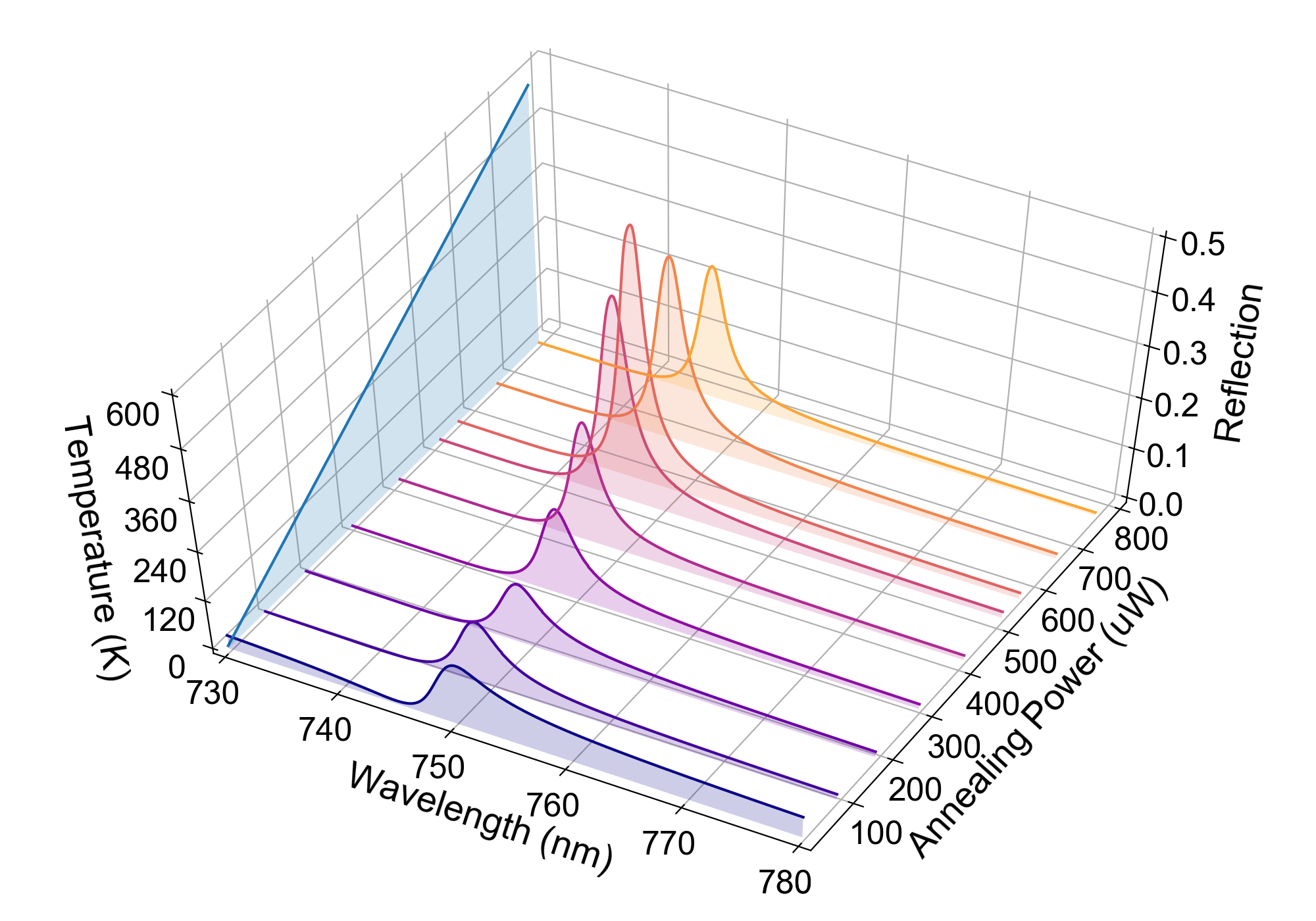
The evolution of the annealed PL and reflection is shown as a function of annealing power in Fig. 4. The and emission disappear at relatively low powers, and the red shift of the exciton primarily occurs at comparable or even lower powers. However, the PL linewidth and peak intensity improve to their best values only at significantly higher powers. The reflection linewidth and peak follow similar trends. The fact that the trion and defect emission are suppressed at relatively low annealing powers could indicate that the doping and defect emission are due to a species of adsorbate that binds less tightly to the layer. However, it is also possible that the linewidth and peak intensity only improve at higher powers simply because they are more sensitive to small amounts of contaminants.
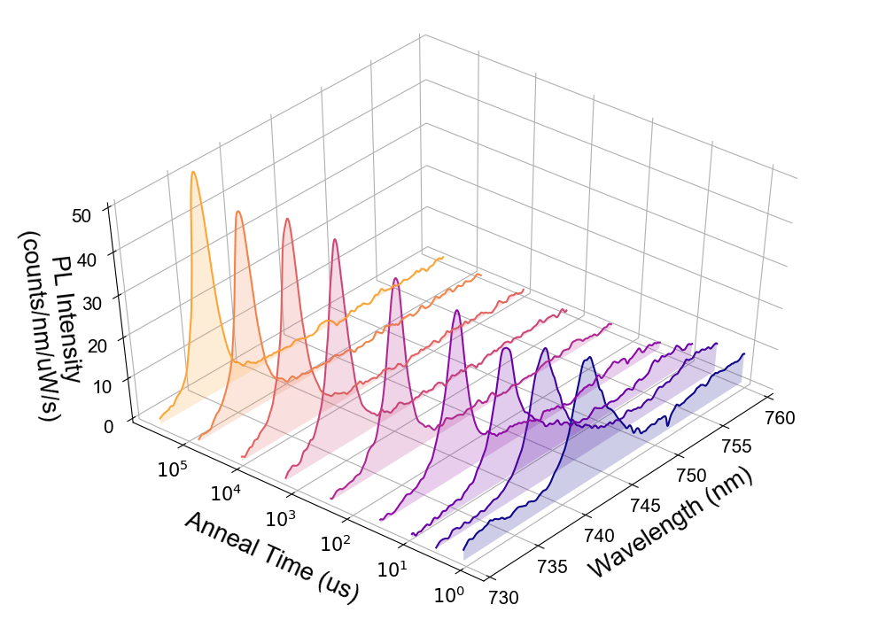
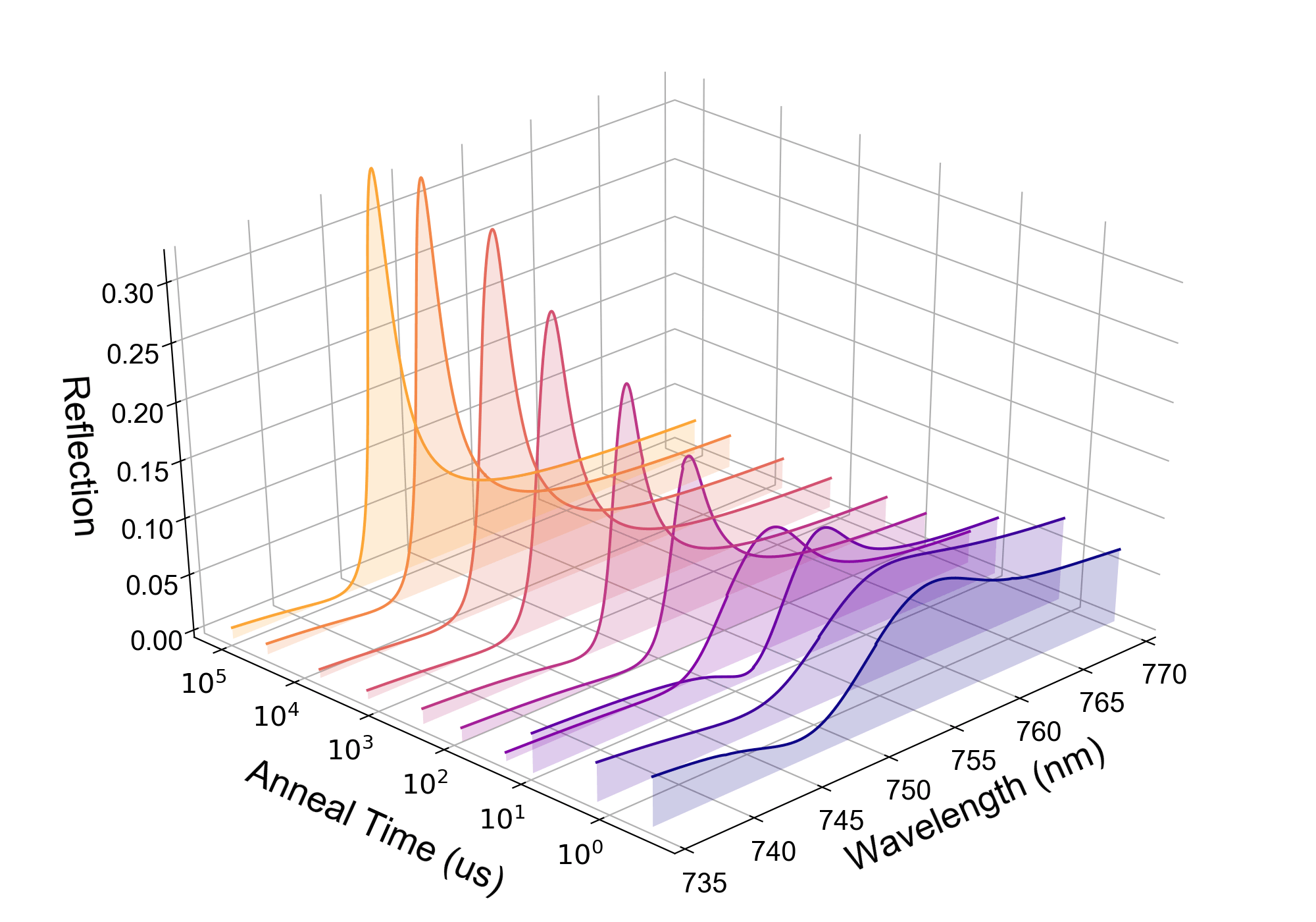
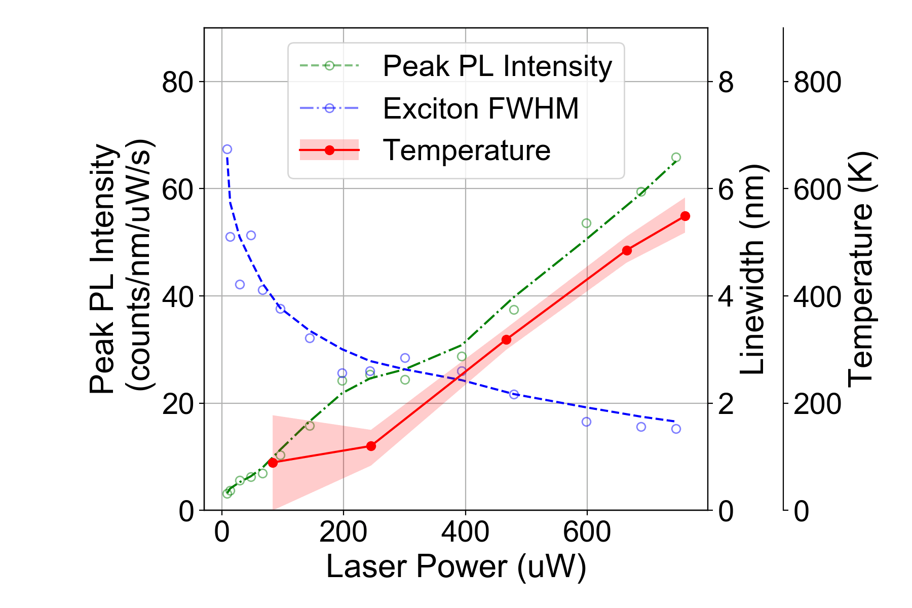
When annealing with a nominally 700 nm diameter spot, the optimal annealing power (as measured by the power at which the PL/reflection linewidths are narrowest) varied from to for the CVD grown samples. Some, but not all, of this variation is likely due to small changes in the focusing conditions between different anneals. As the power was increased, some suspended flakes eventually began to degrade in quality. Others would snap and break before showing any signs of degradation. The PL in Fig. 4a is an example of a film that snapped before degrading, while the reflection in Fig. 4b is an example of a film that degraded before snapping. We posit that the main mode of failure is tearing of the flake due to tensile forces — those flakes with a higher concentration of defects as well as those under more tensile stress from their boundary conditions would break at lower temperatures and lower annealing powers.
The annealing temperature of the suspended measured using Raman thermometry Loudon (1964) is shown in 4c. The maximum temperature for this anneal was about 550 K, and as expected, the temperature varies linearly with excitation power. The PL intensity almost linearly tracks the excitation power.
For comparison, the PL after different-strength anneals and the associated annealing temperatures is shown for a supported flake in Fig. 4d. For the same annealing power, the supported flake does not reach as high temperature during annealing as the suspended flake because of heat conduction into the substrate. The PL of the supported nowhere shows any strong, narrow peak that could definitively be identified as exciton or trion emission. Rather, before annealing it has an extremely broad emission which slowly decreases and somewhat narrows as the annealing power is increased. While at the highest annealing powers there is an extremely faint peak which might in some way be connected to an exciton, the annealing is clearly not effective for supported samples. This could be due to contaminants trapped between the substrate and the that cannot be removed by heating. There may also be roughness and strain pinning due to the substrate which is not affected by the annealing.
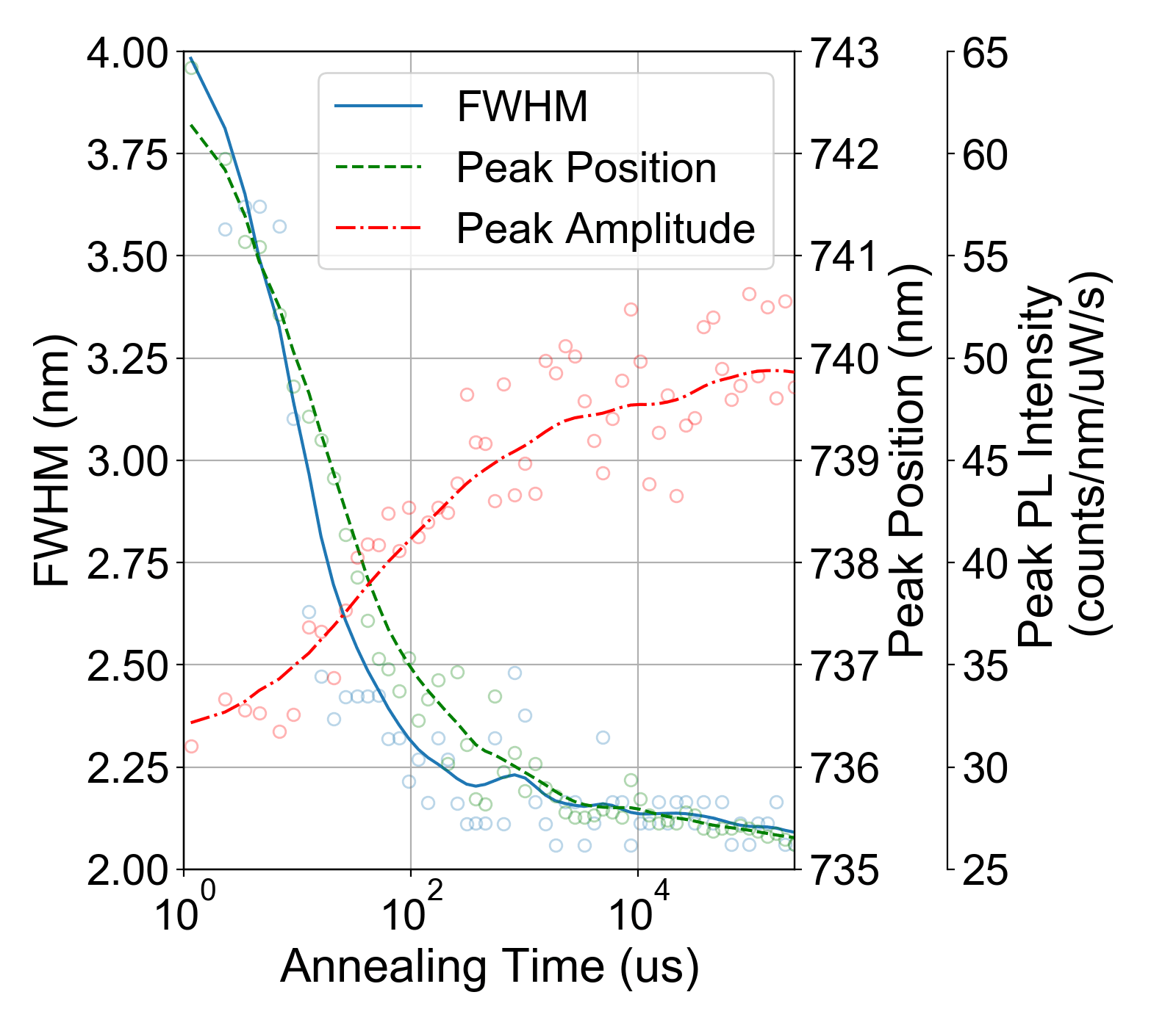
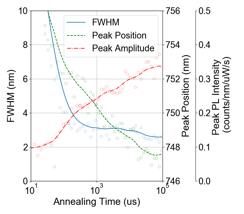
The PL and reflection as a function of annealing time are shown in Fig. 5. The annealing power is kept fixed, and the sample is annealed with pulses. Since the in-plane speed of sound in monolayer should be similar to the m/s speed of Cai et al. (2014), the time to reach thermal equilibrium for a hole with radius is on the order of 7 ns, which is much shorter than the pulse length. This is experimentally supported by the observation that after fully annealing using many pulses, annealing using a CW beam of the same power does not change the PL/reflection of the sample. We can see that the PL improves quite quickly over the first ms, and afterwards changes much more slowly. The blue shift and reduction in broad defect PL both happen even more quickly, in about 10 and 50 , respectively. This is complementary to the fact that the blue shift of the exciton and trion/defect emission suppression occur at low powers in Fig. 4a. On the other hand, the reflection continues to improve even after 10 ms of annealing. This indicates that the peak reflectance is more sensitive and thus a better metric of sample quality than PL. This is supported by Scuri et al. (2018); Back et al. (2018), in which the peak reflectance is shown to be a measure of the ratio of radiative to non-radiative broadening.
III Conclusions
The results presented here strongly indicate that the intrinsic quality of CVD-grown , and by extension other TMDCs including , , and is comparably high to that of their mechanically-exfoliated-from-bulk counterparts. It seems necessary to completely remove contaminants that come from the growth and transfer processes, as well as from the ambient atmosphere. We have shown here that sample quality can be repeatably and dramatically increased, in some cases reaching PL linewidths and peak reflectances close to those of the highest quality encapsulated samples. The homogeneity of the samples appears to be limited by the size of the suspended area, offering a path forward for larger-area homogeneity than yet achieved in exfoliated samples.
We believe that this annealing procedure will enable further studies of exciton-polaritons, cavity QED with excitons, fundamental exciton physics and other many-body physics in TMDCs by providing a repeatable path to high-quality spatially-homogeneous TMDCs (and possibly all 2D materials). This annealing procedure will greatly aid efforts to create high quality arrays of quantum dots for quantum information processing, as well as networks of optical cavities coupled to TMDCs. The repeatability of the annealing as well as the large area and flexibility afforded by CVD-grown samples provides an avenue for scaling to multiple devices. Finally, the annealing procedure may also prove useful for electronic applications through an improvement in carrier mobility.
IV Methods
IV.1 Sample Preparation
The suspended CVD samples were purchased from 2DLayer. Their process involves growing monolayer by CVD, and then transferring to 280 nm SiO2 on Si substrates with patterned holes. The holes were approximately deep and nominally in diameter. The data in all figures except Fig. LABEL:sfig:BeforeAfterSiN was taken using these samples.
A suspended sample was also prepared by starting with bulk from 2D Semiconductor. The flake was exfoliated on to polydimethylsiloxane (PDMS) Castellanos-Gomez et al. (2014), and then directly transferred on to a holey silicon nitride grid from SPI Supplies (2 micron diameter holes in a 50 nm thick silicon nitride membrane). Data from this sample is shown in Fig. LABEL:sfig:BeforeAfterSiN.
IV.2 Experimental Setup
All PL and reflection measurements were performed in a Montana Instruments Cryostation at a nominal base temperature of 4 K. The pressure was typically between and Torr. The cryostat is equipped with an XYZ piezo stage stack from Attocube, on top of which the samples are mounted. A custom microscope assembly looks into the cryostat using a Mitutoyu long-working-distance near-infra-red (NIR) objective with 0.7 mm of glass correction and a numerical aperture (NA) of 0.4. A removable beamsplitter couples light to a wide-field imaging path. See Fig. LABEL:sfig:schematic. There is a 0.5 mm thick glass window on the cryostat, and a 0.2 mm thick glass inner window on the cryostat heat shield, both of which are anti-reflection coated. An XY galvanometer pair is mounted directly behind the objective, which allows scanning of the spot over about . The entire microscope is also mounted on motorized XY translation stages which allow for translation of several mm, as well as a manual Z-stage which is used for focusing the microscope on the sample. Measurements were automated using the python instrument control package Instrumental, available on Github at https://github.com/mabuchilab/Instrumental.
IV.3 PL Measurements
PL was measured by exciting using narrow linewidth ( cm-1 FWHM) 532 nm continuous wave (CW) beam obtained by frequency doubling a 1064 nm pump laser in periodically polled LiNbO3 (PPLN). For the pump, a 10 mW 1064 nm seed from an NKT Koheras Adjustik laser was amplified using a Nufern nuamp amplifier. The 532 nm excitation laser was coupled onto the microscope by a single mode optical fiber and a reflective collimator. It is then coupled into the light path using a volume Bragg grating, which essentially functioned as a dichroic mirror (reflecting 532 nm while transmitting other wavelengths). This separates the PL from the excitation. Again, see Fig. LABEL:sfig:schematic. The excitation is then coupled into another single mode fiber, and the spectrum is measured using a home-built spectrometer. The spectrometer has an 1800 line/mm grating on a computer-controlled rotation stage, and spectra are measured on a Princeton Instruments PIXIS 2048 camera. The nominal resolution of the spectrometer is about 1 cm-1. The excitation power is measured before each spectrum by a power meter on a computer-controlled flip mount in the microscope setup. Typical excitation powers were about at the sample. We did not observe significant changes in line shape when measuring at lower excitation powers.
IV.4 Annealing
The annealing procedure was performed using the same 532 nm laser used for PL, except at much higher powers. The annealing was effective over a large range of spot sizes (we tested from 700 nm to ). As expected, the larger spots required correspondinly more laser power for optimal annealing. We typically annealed using a 700 nm spot for several seconds, although from Fig. 5 it can be seen that the annealing itself occurs in the first few ms. For a beam size of 700 nm the optimal annealing power the optimal annealing power was typically between to .
IV.5 Reflection Measurements
Reflection was measured using a Thorlabs SLS201 broadband stabilized light source. Again, the incident beam was coupled on to the microscope through a single mode fiber. The power at the sample in the range of 700-800 nm was about 5 nW. The reflected beam was separated from the incident beam by a non-polarizing beamsplitter, and was coupled into a single mode fiber. Again, see Fig. LABEL:sfig:schematic. The spectrum was measured using the same spectrometer as for PL. Each reflection spectrum was calibrated by referencing it to the reflection of the bare substrate. The absolute reflection of the bare substrate was measured by in turn referencing to a silver mirror.
IV.6 Reflection Analysis
When measuring reflection spectra from near the center of a suspended monolayer, the small back reflection (between 1% and 3% in most cases) from the bottom of the hole caused etalon interference fringes to appear in the measured spectrum. Even though the reflection was small, the etalon interference fringes were much larger, up to 10%. These fringes make the raw spectra difficult to interpret. Note that this was not an issue for the sample suspended on silicon nitride, since the holes in this case were through holes.
We fit the reflection spectra to a multilayer Fresnel model, which included a reflection from the bottom of the hole to account for the etalon. The dielectric constant of the film was the sum of a real background permittivity and an inhomogenously broadened Lorentzian oscillator to account for interaction with the exciton. Reflection from the trion is ignored, since it is assumed to contribute negligibly to the reflection. This is accurate for all but the highest carrier doping levels Sidler et al. (2016). The background permittivity is meant to account for both the background permittivity of the and any (possibly thick) layer of contaminants. The dielectric permittivity for a Lorentzian oscillator is:
| (1) |
where is the relative permittivity, is the optical frequency, is the center frequency, represents homogenous broadening, and is related to the strength of the oscillator. The permittivity of the exciton is obtained by convolving this Lorentzian with a Gaussian to account for inhomogeneous broadening.
The etalon length (hole depth), etalon reflection, oscillator center frequency, oscillator strength, oscillator homogenous broadening width, oscillator inhomogeneous broadening width, and film background permittivity were all fitted parameters. Once this model was fit to the raw data, the reflection from the suspended film alone could be extracted from the fitting parameters. Examples of the fits to raw data along with the raw data and extracted spectra are shown in Fig. LABEL:sfig:FitExample. The raw spectra for each of the figures in the main text that shows fitted reflection data is also shown in the SI.
IV.7 Thermal Model
The peak temperature during annealing is modeled using a steady-state radial heat equation with the absorption of the laser in the treated as a point heat source. The annealing temperature is calculated as the temperature at one beam radius away from the point source. In the suspended case we set the temperature boundary condition at the edge of the hole to be the nominal base temperature of the cryostat, 4 K. With as the radial temperature distribution, as the heat flux density and the thermal conductivity, the steady state heat equation is:
| (2) |
In the suspended 2D case with the boundary conditions above, the temperature distribution is:
| (3) |
where is the temperature at radius (the beam radius), and is the temperature at (the edge of the hole). For a given input heat flux , the annealing temperature is then:
| (4) |
where is the thickness of the . We use a thermal conductivity of 40 W/mK for the , which is consistent with both theory and experiment Hong et al. (2016); Zhang et al. (2015).
The supported case follows a similar analysis, except in this case we use infinite boundary conditions (the temperature goes to 4 K at large radius), and we assume that the thermal conductivity of the substrate dominates that of the flake. In this case, the annealing temperature is:
| (5) |
We use a thermal conductivity of 2 W/mK for the substrate, which is intermediate between that of and Si (but closer to that of ) in the relevant temperature range Glassbrenner and Slack (1964); Yao et al. (2008). The laser spot diameter was nm, and the hole radius was . Note that both models above ignore any temperature dependence of the thermal conductivity.
IV.8 Raman Thermometry
Raman measurements were performed using the same 532 nm laser and the same beam path as for the PL measurements, except that an extra volume Bragg grating was used on the microscope to further knock out the excitation laser. This was necessary to prevent fiber Raman from overwhelming the Raman scattering from the , since the microscope was coupled to the spectrometer using a single mode fiber. A different home-built spectrometer was used for Raman measurements. This spectrometer has a 1200 line/mm blazed grating, and spectra are measured using a PIXIS 256 camera. The nominal resolution is about 1.5 cm-1. There are two more volume Bragg gratings within the spectrometer, to further knock out the 532 nm excitation.
We used the raman peak at 242 cm-1 to perform Raman thermometry during the annealing process. Since the annealing process was in most cases at relatively low laser powers, the scattering signal was very weak and typical spectra would involve up to 10 exposures of 20 minutes each. The ratio between Stokes and anti-Stokes scattering is:
| (6) |
where and are respectively the Stokes and anti-Stokes intensities, is the laser frequency, is the Raman transition frequency, is the temperature, is Planck’s constant and is the Boltzmann constant. The temperature is then:
| (7) |
Some examples of the Raman spectra used in calculating the annealing temperature are shown in Fig. LABEL:sfig:raman.
IV.9 XPS
We took XPS data from a supported area, assuming that the contaminants are qualitatively similar on suspended and supported areas. Data was taken on a PHI Versaprobe 3, on a monolayer of dimensions using a X-ray spot. This instrument uses 1486 eV X-rays and is sensitive to the top of the sample. We used the machine calibration to extract atomic abundances using MultiPak software. A bulk sample of from HQ Graphene was used as a further calibration for the relative abundance of Mo and Se. The raw XPS data for a supported flake is shown in Fig. LABEL:sfig:XPS:Spectrum.
Acknowledgements.
This work was funded in part by the National Science Foundation (NSF) award PHY-1648807, and also by a seed grant from the Precourt Institute for Energy at Stanford University. Part of this work was performed at the Stanford Nano Shared Facilities (SNSF), supported by the NSF under award ECCS-1542152. CR, DG, and NB were supported in part by Stanford Graduate Fellowships. CR was also supported in part by a Natural Sciences and Engineering Research Council of Canada doctoral postgraduate scholarship. CR thanks Charles Hitzman for help performing and interpreting the XPS data. CR also thanks Ozgur Burak Aslan for discussions of strain effects in TMDC materials.V Author Contributions
CR first noted the annealing effect, conceived the experiments, performed the experiments and performed the data analysis. HM suggested raster scanning the anneal, and annealing with a large diameter beam. CR and DG built the reflection/PL/raman microscope setup, as well as the custom spectrometers. DG built the frequency doubling setup. CR and NB automated the measurements. All authors contributed to the manuscript.
References
- Mak et al. (2010) Kin Fai Mak, Changgu Lee, James Hone, Jie Shan, and Tony F. Heinz, “Atomically thin : A new direct-gap semiconductor,” Phys. Rev. Lett. 105, 136805 (2010).
- Splendiani et al. (2010) Andrea Splendiani, Liang Sun, Yuanbo Zhang, Tianshu Li, Jonghwan Kim, Chi-Yung Chim, Giulia Galli, and Feng Wang, “Emerging photoluminescence in monolayer mos2,” Nano Letters 10, 1271–1275 (2010).
- Jones et al. (2013) Aaron M. Jones, Hongyi Yu, Nirmal J. Ghimire, Sanfeng Wu, Grant Aivazian, Jason S. Ross, Bo Zhao, Jiaqiang Yan, David G. Mandrus, Di Xiao, Wang Yao, and Xiaodong Xu, “Optical generation of excitonic valley coherence in monolayer wse2,” Nature Nanotechnology 8, 634 EP – (2013).
- Xiao et al. (2012) Di Xiao, Gui-Bin Liu, Wanxiang Feng, Xiaodong Xu, and Wang Yao, “Coupled spin and valley physics in monolayers of and other group-vi dichalcogenides,” Phys. Rev. Lett. 108, 196802 (2012).
- Mak et al. (2012a) Kin Fai Mak, Keliang He, Jie Shan, and Tony F. Heinz, “Control of valley polarization in monolayer mos2 by optical helicity,” Nature Nanotechnology 7, 494 EP – (2012a).
- Conley et al. (2013) Hiram J. Conley, Bin Wang, Jed I. Ziegler, Richard F. Haglund, Sokrates T. Pantelides, and Kirill I. Bolotin, “Bandgap engineering of strained monolayer and bilayer mos2,” Nano Letters 13, 3626–3630 (2013).
- You et al. (2015) Yumeng You, Xiao-Xiao Zhang, Timothy C. Berkelbach, Mark S. Hybertsen, David R. Reichman, and Tony F. Heinz, “Observation of biexcitons in monolayer wse2,” Nature Physics 11, 477 EP – (2015).
- Sidler et al. (2016) Meinrad Sidler, Patrick Back, Ovidiu Cotlet, Ajit Srivastava, Thomas Fink, Martin Kroner, Eugene Demler, and Atac Imamoglu, “Fermi polaron-polaritons in charge-tunable atomically thin semiconductors,” Nature Physics 13, 255 EP – (2016).
- Wang et al. (2018) Ke Wang, Kristiaan De Greve, Luis A. Jauregui, Andrey Sushko, Alexander High, You Zhou, Giovanni Scuri, Takashi Taniguchi, Kenji Watanabe, Mikhail D. Lukin, Hongkun Park, and Philip Kim, “Electrical control of charged carriers and excitons in atomically thin materials,” Nature Nanotechnology 13, 128–132 (2018).
- Palacios-Berraquero et al. (2017) Carmen Palacios-Berraquero, Dhiren M. Kara, Alejandro R. P Montblanch, Matteo Barbone, Pawel Latawiec, Duhee Yoon, Anna K. Ott, Marko Loncar, Andrea C. Ferrari, and Mete Atatüre, “Large-scale quantum-emitter arrays in atomically thin semiconductors,” Nature Communications 8, 15093 EP – (2017), article.
- Mak et al. (2012b) Kin Fai Mak, Keliang He, Changgu Lee, Gwan Hyoung Lee, James Hone, Tony F. Heinz, and Jie Shan, “Tightly bound trions in monolayer mos2,” Nature Materials 12, 207 EP – (2012b).
- Cadiz et al. (2017) F. Cadiz, E. Courtade, C. Robert, G. Wang, Y. Shen, H. Cai, T. Taniguchi, K. Watanabe, H. Carrere, D. Lagarde, M. Manca, T. Amand, P. Renucci, S. Tongay, X. Marie, and B. Urbaszek, “Excitonic linewidth approaching the homogeneous limit in -based van der waals heterostructures,” Phys. Rev. X 7, 021026 (2017).
- Scuri et al. (2018) Giovanni Scuri, You Zhou, Alexander A. High, Dominik S. Wild, Chi Shu, Kristiaan De Greve, Luis A. Jauregui, Takashi Taniguchi, Kenji Watanabe, Philip Kim, Mikhail D. Lukin, and Hongkun Park, “Large excitonic reflectivity of monolayer encapsulated in hexagonal boron nitride,” Phys. Rev. Lett. 120, 037402 (2018).
- Back et al. (2018) Patrick Back, Sina Zeytinoglu, Aroosa Ijaz, Martin Kroner, and Atac Imamoğlu, “Realization of an electrically tunable narrow-bandwidth atomically thin mirror using monolayer ,” Phys. Rev. Lett. 120, 037401 (2018).
- Mennel et al. (2018) Lukas Mennel, Marco M. Furchi, Stefan Wachter, Matthias Paur, Dmitry K. Polyushkin, and Thomas Mueller, “Optical imaging of strain in two-dimensional crystals,” Nature Communications 9, 516 (2018).
- Hong et al. (2015) Jinhua Hong, Zhixin Hu, Matt Probert, Kun Li, Danhui Lv, Xinan Yang, Lin Gu, Nannan Mao, Qingliang Feng, Liming Xie, Jin Zhang, Dianzhong Wu, Zhiyong Zhang, Chuanhong Jin, Wei Ji, Xixiang Zhang, Jun Yuan, and Ze Zhang, “Exploring atomic defects in molybdenum disulphide monolayers,” Nature Communications 6, 6293 EP – (2015), article.
- Wang et al. (2015) Haining Wang, Changjian Zhang, and Farhan Rana, “Ultrafast dynamics of defect-assisted electron-hole recombination in monolayer mos2,” Nano Letters 15, 339–345 (2015).
- Xue et al. (2011) Jiamin Xue, Javier Sanchez-Yamagishi, Danny Bulmash, Philippe Jacquod, Aparna Deshpande, K. Watanabe, T. Taniguchi, Pablo Jarillo-Herrero, and Brian J. LeRoy, “Scanning tunnelling microscopy and spectroscopy of ultra-flat graphene on hexagonal boron nitride,” Nature Materials 10, 282 EP – (2011).
- Yu et al. (2013) Yifei Yu, Chun Li, Yi Liu, Liqin Su, Yong Zhang, and Linyou Cao, “Controlled scalable synthesis of uniform, high-quality monolayer and few-layer mos2 films,” Scientific Reports 3, 1866 EP – (2013), article.
- (20) Yi‐Hsien Lee, Xin‐Quan Zhang, Wenjing Zhang, Mu‐Tung Chang, Cheng‐Te Lin, Kai‐Di Chang, Ya‐Chu Yu, Jacob Tse‐Wei Wang, Chia‐Seng Chang, Lain‐Jong Li, and Tsung‐Wu Lin, “Synthesis of large‐area mos2 atomic layers with chemical vapor deposition,” Advanced Materials 24, 2320–2325.
- Nan et al. (2014) Haiyan Nan, Zilu Wang, Wenhui Wang, Zheng Liang, Yan Lu, Qian Chen, Daowei He, Pingheng Tan, Feng Miao, Xinran Wang, Jinlan Wang, and Zhenhua Ni, “Strong photoluminescence enhancement of mos2 through defect engineering and oxygen bonding,” ACS Nano 8, 5738–5745 (2014).
- Wood et al. (2015) Joshua D Wood, Gregory P Doidge, Enrique A Carrion, Justin C Koepke, Joshua A Kaitz, Isha Datye, Ashkan Behnam, Jayan Hewaparakrama, Basil Aruin, Yaofeng Chen, Hefei Dong, Richard T Haasch, Joseph W Lyding, and Eric Pop, “Annealing free, clean graphene transfer using alternative polymer scaffolds,” Nanotechnology 26, 055302 (2015).
- Amani et al. (2016) Matin Amani, Robert A. Burke, Xiang Ji, Peida Zhao, Der-Hsien Lien, Peyman Taheri, Geun Ho Ahn, Daisuke Kirya, Joel W. Ager, Eli Yablonovitch, Jing Kong, Madan Dubey, and Ali Javey, “High luminescence efficiency in mos2 grown by chemical vapor deposition,” ACS Nano 10, 6535–6541 (2016).
- Florian et al. (2018) Matthias Florian, Malte Hartmann, Alexander Steinhoff, Julian Klein, Alexander W. Holleitner, Jonathan J. Finley, Tim O. Wehling, Michael Kaniber, and Christopher Gies, “The dielectric impact of layer distances on exciton and trion binding energies in van der waals heterostructures,” Nano Letters 18, 2725–2732 (2018).
- Robert et al. (2016) C. Robert, D. Lagarde, F. Cadiz, G. Wang, B. Lassagne, T. Amand, A. Balocchi, P. Renucci, S. Tongay, B. Urbaszek, and X. Marie, “Exciton radiative lifetime in transition metal dichalcogenide monolayers,” Phys. Rev. B 93, 205423 (2016).
- Tongay et al. (2013) Sefaattin Tongay, Jian Zhou, Can Ataca, Jonathan Liu, Jeong Seuk Kang, Tyler S. Matthews, Long You, Jingbo Li, Jeffrey C. Grossman, and Junqiao Wu, “Broad-range modulation of light emission in two-dimensional semiconductors by molecular physisorption gating,” Nano Letters 13, 2831–2836 (2013).
- Li et al. (2014) Yilei Li, Alexey Chernikov, Xian Zhang, Albert Rigosi, Heather M. Hill, Arend M. van der Zande, Daniel A. Chenet, En-Min Shih, James Hone, and Tony F. Heinz, “Measurement of the optical dielectric function of monolayer transition-metal dichalcogenides: , , , and ,” Phys. Rev. B 90, 205422 (2014).
- Loudon (1964) R. Loudon, “The raman effect in crystals,” Advances in Physics 13, 423–482 (1964).
- Cai et al. (2014) Yongqing Cai, Jinghua Lan, Gang Zhang, and Yong-Wei Zhang, “Lattice vibrational modes and phonon thermal conductivity of monolayer mos2,” Phys. Rev. B 89, 035438 (2014).
- Castellanos-Gomez et al. (2014) Andres Castellanos-Gomez, Michele Buscema, Rianda Molenaar, Vibhor Singh, Laurens Janssen, Herre S J van der Zant, and Gary A Steele, “Deterministic transfer of two-dimensional materials by all-dry viscoelastic stamping,” 2D Materials 1, 011002 (2014).
- Hong et al. (2016) Yang Hong, Jingchao Zhang, and Xiao Cheng Zeng, “Thermal conductivity of monolayer mose2 and mos2,” The Journal of Physical Chemistry C 120, 26067–26075 (2016).
- Zhang et al. (2015) Xian Zhang, Dezheng Sun, Yilei Li, Gwan-Hyoung Lee, Xu Cui, Daniel Chenet, Yumeng You, Tony F. Heinz, and James C. Hone, “Measurement of lateral and interfacial thermal conductivity of single- and bilayer mos2 and mose2 using refined optothermal raman technique,” ACS Applied Materials & Interfaces 7, 25923–25929 (2015).
- Glassbrenner and Slack (1964) C. J. Glassbrenner and Glen A. Slack, “Thermal conductivity of silicon and germanium from k to the melting point,” Phys. Rev. 134, A1058–A1069 (1964).
- Yao et al. (2008) Da-Jeng Yao, Wei-Chih Lai, and Heng-Chieh Chien, “Temperature dependence of thermal conductivity for silicon dioxide,” 2008 Proceedings of the ASME Micro/Nanoscale Heat Transfer International Conference, MNHT 2008 , 435–439 (2008).