Redox reaction enhanced Schottky contact at a LaNiO3(001)/Al interface
Abstract
Emergent phenomena at interfaces between oxides and metals can appear due to charge transfer and mass transport that modify the bulk properties. By coating the metallic oxide LaNiO3 by aluminium, we fabricated a junction exhibiting a diode-like behaviour. At the equilibrium, the interface is insulating. The metallic behaviour can be recovered by applying a voltage drop across the junction in one polarity only. The electrical properties in direct and reverse bias are investigated. The observed electro-resistive effect rises up to % and can be interpreted in terms of (i) a spontaneous redox reaction occurring at the interface and (ii) its reversal induced by charge injection in direct bias.
I Introduction
Oxide surfaces and interfaces attract a growing attention due to the emergence of several phenomena which are absent in the bulk. Progress in synthesis of thin films enabled to get rid of extrinsic factor like surface roughness or grain boundaries and the engineering of heterostructure of ultra-thin films has become a new way to manipulate the electronic structure at the surfaces and interfaces.
Nickelates offer an ideal background for the emergence of surface and interface phenomena : (i) their ground state is close to a metal-to-insulator transition (MIT) that occur between 100 and 600 K depending of the rare earth ionic radius (except LaNiO3 that remains metallic at the lowest temperature) [8, 27]; (ii) nickel sites are magnetic and order at low temperature [10]; (iii) their electronic structures are strongly coupled with structural distortions due to their electron correlations; (iv) the valence band is degenerated and has a hybridized Ni and O character that makes them charge transfer insulators in the insulating side of the MIT : hence, not only does oxygen vacancy distort the ionic lattice but it directly affect the filling of the valence band as well [26].
Proper epitaxial strain have proved to lift the orbital degeneracy [4, 19, 11] resulting in orbital polarization of the electronic structure [20]. The band structure can also be tailored by the breaking of the translational invariance at a surface or an interface causes a charge redistribution thus creating an electronic structure different from that of the bulk [6]. Surface termination layer can be chosen to adjust the surface electronic state via surface electrostatic properties [16]. Emergent surface magnetic order at the interface between non magnetic compounds have been reported too [9].
In the case of an metal-oxide interface, mass transport can occur and modify the charge transfer. If the mass transport takes place over more than one monolayer, the situation can be described in terms of a chemical interaction (redox reaction, alloy formation, encapsulation or interdiffusion) yielding new compounds that intervene in the charge redistribution [7]. This principle has been recently applied in a universal method to fabricate 2D electron systems with insulating oxides [21]. Used on metallic LaNiO3 this method leads to an electro-resistive effect reported in Ref. [24].
Here, we describe the reduction of an oxide by an aluminium overlayer deposited on a the metallic oxide LaNiO3. The latter compound hosts a metal-to-insulator transition as oxygen vacancies are introduced in the material [2, 3]. The electric properties of the individual compounds of the Al/LaNiO3 interface are dramatically modified by the solid phase redox reaction that take place. The reaction can be explained in terms of transport of oxygen ions through the interface. We show that the reaction can be reversed by an external electric field and the junction resistance varies by a factor up to 1000.
II Experimental procedure
The LaNiO3 films were epitaxially grown on (001) SrTiO3 substrates by pulsed laser deposition and subsequently annealed during 45 min under oxygen. The growth procedure and the quality of the film are reported in Ref. [1, 3] The oxygen stoichiometry of the LaNiO3-δ films could be estimated by a direct procedure described in [23] and the average is found to be less than 0.2 here. A 80 nm thick Al overlayer was then deposited by using a rf-sputtering on three LaNiO3 films having three different thickness (6, 10 and 16 nm).
The electrical properties were probed in a standard 2-wire configuration.
III Results
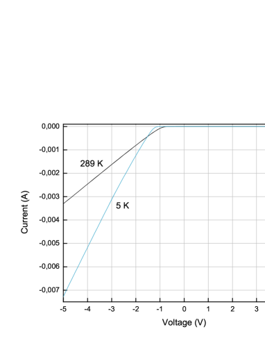
The curves of the three measured junctions exhibit a diode-like behaviour illustrated in Fig. 1. The transition is fully reversible and was observed to be stable over tens of cycles. At low temperature, the change of resistance with the sign of the voltage is significantly enhanced.
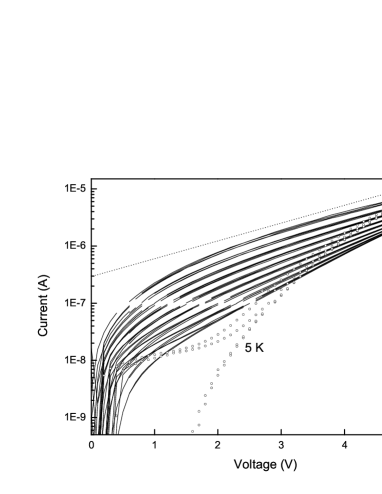
For reverse bias, the current increases with the voltage following an exponential trend (figure 2). As the junctions are cooled down, the curves in log scale are shifted toward higher resistance. Those properties can be coherently modelled by a tunnel junction in series with an insulator. Below 175 K, the curves progressively deviate from the high temperature behaviour. This deviation can be accounted for by a thermoelectric current : each copper wire of the voltage probes makes a heterogeneous contact between distinct conductors at distinct temperatures. As the circuit is closed by the ammeter and the junction cooled down, a thermocouple current adds to the conduction current induced by the applied voltage. In reverse bias, where the conduction current is vanishing at low temperature, the contribution of the thermoelectric current to the measured current is expected to be significant. This spurious effect renders the low temperature data little reliable and the discussion will be restricted to the data above 175 K where the temperature gradient is moderate.
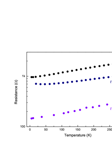
The electrical properties in direct bias are represented by the temperature dependence of the resistance measured at the applied voltage V. The residual resistivity ratios range between 1.6 and 2.0 and the estimated resistivity upper bounds (assuming conductive path is about 1 mm long, 3 mm wide and at most as thick as the LaNiO3 layer) are 3000 cm for the 6 and 10 nm samples and 1000 cm for the 16 nm sample. Those values are coherent with the literature and one order magnitude above the most conducting single crystals [10] and thick films [15]. Also, the resistance of the junction indirect bias agrees well with that of the LaNiO3 film away from the Al over-layer.
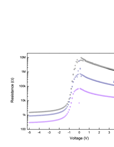
The thickness dependence of the electro-resistive effect is reported in Fig. 4. Electro-resistive effect decreases as the LaNiO3 layer increases. More precisely, the resistance in the reverse bias is much more enhanced than in direct bias as the thickness is diminished. This trend shows that the oxygen vacancies created by the oxidization of Al are concentrated at the interface: the thicker the LaNiO3 layer is, the thicker is the conducting path through metallic, i.e. stoichiometric, LaNiO3. This is coherent with Tian et al. who demonstrated that Ni valence is reduced below 3+ only in the first 10 nm of LaNiO3 below the interface. The conducting path for reverse bias can be sketched by a tunnel junction in series with two resistors in parallel representing the semiconducting LaNiO3-δ and the metallic LaNiO3 layers (Fig. 5-a and b).
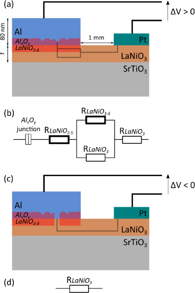
In contrast, the electric behaviour in the direct bias is metallic. It is as though conducting channels opened through the AlOx/LaNiO2.5 bi-layer by a local healing of the Al/LaNiO3 interface (Fig. 5-c and d).
IV Discussion
In this section, the results will be discussed and arguments will be brought to justify the interpretation of the electro-resistive effect in terms of redox reaction controlled by the external electric field.
The shape of the curve corresponds to a typical Schottky diode characteristics. However, in this model, the resistance in the reverse bias is expected to grow, or at least not to exponentially decrease, with the voltage. Aluminium is well-known to be a strong reducing agent that pumps oxygen out of the oxide it is deposited on [7]. A direct evidence of the concomitant oxidization of Al and reduction of LaNiO3 at a Al/LaNiO3 contact have been brought in Ref. [24]. Thus, the situation can not be described as a regular Schottky contact because of the mass transport which is not considered in this model.
As the Al-LaNiO3 contact is formed, electrons are driven from the metal to the oxide by the gradient of chemical potential since [12, 13]. The electrons diffusing in the oxide combine with mobile holes and fill the nearly filled Ni-O band that crosses the Fermi level in LaNiO3 [14]. The oxide is turned a semiconductor. The states the extra electrons set in have been calculated to have an oxygen character [17]. This favours the mobility of oxygen ions. Thus, the charge carried by the diffusion electrons drives O2- ions outward the oxide where a vacancy is formed and toward the metal where an AlxOy aluminium oxide layer is formed. The oxygen transport through the oxide and across the interface is favoured by (i) the high mobility of oxygen in LaNiO3 (activation barrier of oxygen is 0.65-0.80 eV depending of the tensile strain [18]), (ii) the thermodynamic stability of oxygen off-stoichiometric phases LaNiO2.75 and LaNiO2.5 [5, 22]. Such formation and spontaneous arrangement of oxygen vacancies have been shown to be an energetically favourable response of the lattice in presence of electrostatic charge [25].
Finally, the contact between a metal and a metallic oxide makes a highly resistive junction at the equilibrium because of the spontaneous formation of two stable, neutral and insulating layers of AlxOy and LaNiO3-δ between the LaNiO3 and the Al layers.
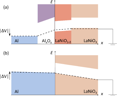
The band diagrams for reverse and direct bias can be sketched as in Fig. 6. In reverse bias, mobile charge carriers are strongly suppressed by the opening of a band gap in the intermediate compounds formed at the interface by the redox reaction. Furthermore, the ionic conduction is impeded by the absence (i) of mobile oxygen ions in LaNiO3-δ and (ii) of available oxygen sites in AlxOy. The response of the junction to the applied voltage in reverse bias is the bending the bands in AlxOy and to some extent in LaNiO3-δ (figure 6-a). In this scheme, the reverse bias can be described as the tunnelling of carriers through the AlxOy/LaNiO3-δ barrier whose effective height of the barrier decreases as the applied voltage increases. Its width may be smaller than the average thickness of the AlxOy/LaNiO3-δ bi-layer due to interface roughness. From transmission electron microscopy led on analogue systems in Ref. [24], the AlxOy thickness can be estimated to be about 10 nm, with enough roughness for weak spots as thin as a few nanometres can exist. The two compounds yielded by the solid phase redox reaction should have defects so that multiple tunnelling through those defects is likely to take place too. This would lower the effective width of the barrier and explain why the curves depart from the behaviour of a simple tunnel junction. In this context, it is difficult to precisely estimate the active area. The rather surprising reversibility of the electro-resistance process suggests that only little mass is transported, and hence that the area is relatively small.
In direct bias, the applied electric field drives O2- ions from the aluminium oxide toward the nickelate as well as the free holes from LaNiO3 toward the LaNiO3-δ layer. The holes injected in LaNiO3 combine with nickel electrons and promote Ni host valence to 3+. This creates available oxygen sites where O2- ions will be driven to satisfy the octahedral coordination of Ni3+ sites. This two-fold transfer of charge and mass turns out to reverse the redox reaction by reducing the aluminium oxide and re-oxidizing LaNiO3. Above a threshold voltage, the metallic behaviour is recovered all along the conducting path. The insulator-to-metal transition occurs over a 2 V-wide interval of applied voltages centred around a threshold value of 0.7-0.8 V (resp. 0.8-0.9 V) at room temperature (resp. at 5 K), taking the criterion of a division by 10 of the maximum resistance.
V Conclusions
We reported the electrical behaviour of a Al/LaNiO3 contact. Both charge and mass transfer take place in this metal-oxide contact and the Schottky effect is strongly enhanced. Due to the occurrence of a redox reaction, insulating intermediate compounds are formed at the interface between those two metallic native compounds and the junction is highly resistive at the equilibrium. The junction exhibits either tunnelling-like conduction or a metallic behaviour depending on the sign of the applied voltage. The fabrication of such a junction is straightforward with basic growth tools, inexpensive, efficient at room temperature. On top of that, the mass transfer is found to be confined to a few nanometres around the interface. All these features makes this system promising for applications in nano-electronics.
VI Acknowledgement
This work was supported by the Ile-de-France region for magneto-transport measurements ("NOVATECS" C’Nano IdF project n∘ IF-08-1453/R)
References
- [1] B. Berini, W. Noun, Y. Dumont, E. Popova, and N. Keller. High temperature ellipsometry of the conductive oxide lanio3. Journal of Applied Physics, 101(2), 2007.
- [2] Bruno Berini, Niels Keller, Yves Dumont, Elena Popova, Wafaa Noun, Marcel Guyot, Jacky Vigneron, Arnaud Etcheberry, Nuno Franco, and Rui M. C. da Silva. Reversible phase transformation of thin films studied in situ by spectroscopic ellipsometry. Phys. Rev. B, 76:205417, Nov 2007.
- [3] Bruno Berini, Niels Keller, Benjamin Pigeau, Yves Dumont, Elena Popova, Nuno Franco, and Rui M. C. da Silva. Tuning of oxidation states in the lanio3-δ perovskite around the insulator-metal transition. Journal of Applied Physics, 104(10), 2008.
- [4] J. Chakhalian, J. M. Rondinelli, Jian Liu, B. A. Gray, M. Kareev, E. J. Moon, N. Prasai, J. L. Cohn, M. Varela, I. C. Tung, M. J. Bedzyk, S. G. Altendorf, F. Strigari, B. Dabrowski, L. H. Tjeng, P. J. Ryan, and J. W. Freeland. Asymmetric orbital-lattice interactions in ultrathin correlated oxide films. Phys. Rev. Lett., 107:116805, Sep 2011.
- [5] Michel Crespin, Pierre Levitz, and Lucien Gatineau. Reduced forms of lanio3 perovskite. part 1.-evidence for new phases: La2ni2o5 and lanio2. J. Chem. Soc., Faraday Trans. 2, 79:1181–1194, 1983.
- [6] Ankit S. Disa, Divine P. Kumah, Andrei Malashevich, Hanghui Chen, Dario A. Arena, Eliot D. Specht, Sohrab Ismail-Beigi, F. J. Walker, and Charles H. Ahn. Orbital engineering in symmetry-breaking polar heterostructures. Phys. Rev. Lett., 114:026801, Jan 2015.
- [7] Qiang Fu and Thomas Wagner. Interaction of nanostructured metal overlayers with oxide surfaces. Surface Science Reports, 62(11):431 – 498, 2007.
- [8] J. L. García-Muñoz, J. Rodríguez-Carvajal, and P. Lacorre. Neutron-diffraction study of the magnetic ordering in the insulating regime of the perovskites r (r=pr and nd). Phys. Rev. B, 50:978–992, Jul 1994.
- [9] Marta Gibert, Pavlo Zubko, Raoul Scherwitzl, Jorge iguez, and Jean-Marc Triscone. Exchange bias in lanio3?lamno3 superlattices. Nature Materials, 11:195, 2012.
- [10] H. Guo, Z. W. Li, L. Zhao, Z. Hu, C. F. Chang, C.-Y. Kuo, W. Schmidt, A. Piovano, T. W. Pi, O. Sobolev, D. I. Khomskii, L. H. Tjeng, and A. C. Komarek. Antiferromagnetic correlations in the metallic strongly correlated transition metal oxide lanio3. Nature Communications, 9:43, 2018.
- [11] Zhuoran He and Andrew J. Millis. Strain control of electronic phase in rare-earth nickelates. Phys. Rev. B, 91:195138, May 2015.
- [12] Wesley T. Hong, Kelsey A. Stoerzinger, Brian Moritz, Thomas P. Devereaux, Wanli Yang, and Yang Shao-Horn. Probing lamo3 metal and oxygen partial density of states using x-ray emission, absorption, and photoelectron spectroscopy. The Journal of Physical Chemistry C, 119(4):2063–2072, 2015.
- [13] Ryan Jacobs, John Booske, and Dane Morgan. Understanding and controlling the work function of perovskite oxides using density functional theory. Advanced Functional Materials, 26(30):5471–5482, 2016.
- [14] Daniel I. Khomskii. Transition Metal Compounds. Cambridge University Press, 2014.
- [15] P. D. C. King, H. I. Wei, Y. F. Nie, M. Uchida, C. Adamo, S. Zhu, X. He, I. Bo?ovi?, D. G. Schlom, and K. M. Shen. Atomic-scale control of competing electronic phases in ultrathin lanio3. Nature Nanotehcnology, 9:443, 2014.
- [16] Divine P. Kumah, Andrei Malashevich, Ankit S. Disa, Dario A. Arena, Frederick J. Walker, Sohrab Ismail-Beigi, and Charles H. Ahn. Effect of surface termination on the electronic properties of films. Phys. Rev. Applied, 2:054004, Nov 2014.
- [17] Andrei Malashevich and Sohrab Ismail-Beigi. First-principles study of oxygen-deficient structures. Phys. Rev. B, 92:144102, Oct 2015.
- [18] Tam Mayeshiba and Dane Morgan. Strain effects on oxygen migration in perovskites. Phys. Chem. Chem. Phys., 17:2715–2721, 2015.
- [19] E. A. Nowadnick, J. P. Ruf, H. Park, P. D. C. King, D. G. Schlom, K. M. Shen, and A. J. Millis. Quantifying electronic correlation strength in a complex oxide: A combined dmft and arpes study of . Phys. Rev. B, 92:245109, Dec 2015.
- [20] Oleg E. Peil, Michel Ferrero, and Antoine Georges. Orbital polarization in strained : Structural distortions and correlation effects. Phys. Rev. B, 90:045128, Jul 2014.
- [21] Tobias Chris R del, Franck Fortuna, Shamashis Sengupta, Emmanouil Frantzeskakis, Patrick Le F vre, Fran ois Bertran, Bernard Mercey, Sylvia Matzen, Guillaume Agnus, Thomas Maroutian, Philippe Lecoeur, and Andr s Felipe Santander-Syro. Universal fabrication of 2d electron systems in functional oxides. Advanced Materials, 28(10):1976–1980, 2016.
- [22] R. D. Sánchez, M. T. Causa, A. Caneiro, A. Butera, M. Vallet-Regí, M. J. Sayagués, J. González-Calbet, F. García-Sanz, and J. Rivas. Metal-insulator transition in oxygen-deficient perovskites. Phys. Rev. B, 54:16574–16578, Dec 1996.
- [23] J Scola, A Benamar, B Berini, F Jomard, and Y Dumont. Direct measurement of oxygen stoichiometry in perovskite films. Journal of Physics D: Applied Physics, 50(4):045302, 2017.
- [24] Bobo Tian, Pavan Nukala, Mohamed Ben Hassine, Xiaolin Zhao, Xudong Wang, Hong Shen, Jianlu Wang, Shuo Sun, Tie Lin, Jinglan Sun, Jun Ge, Rong Huang, Chungang Duan, Thomas Reiss, Maria Varela, Brahim Dkhil, Xiangjian Meng, and Junhao Chu. Interfacial memristors in al-lanio3 heterostructures. Phys. Chem. Chem. Phys., 19:16960–16968, 2017.
- [25] I-Cheng Tung, Guangfu Luo, June Hyuk Lee, Seo Hyoung Chang, Jarrett Moyer, Hawoong Hong, Michael J. Bedzyk, Hua Zhou, Dane Morgan, Dillon D. Fong, and John W. Freeland. Polarity-driven oxygen vacancy formation in ultrathin films on . Phys. Rev. Materials, 1:053404, Oct 2017.
- [26] J. Zaanen, G. A. Sawatzky, and J. W. Allen. Band gaps and electronic structure of transition-metal compounds. Phys. Rev. Lett., 55:418–421, Jul 1985.
- [27] J.-S. Zhou, J. B. Goodenough, and B. Dabrowski. Transition from curie-weiss to enhanced pauli paramagnetism in . Phys. Rev. B, 67:020404, Jan 2003.