Optimizing thermoelectric efficiency of superlattice nanowires at room temperature
Abstract
It is known that the figure of merit () of thin nanowires can be significantly enhanced at room temperature due to the reduction of phonon thermal conductance arising from the increase of boundary scattering of phonons. It is expected that the phonon thermal conductance of nanowires filled with quantum dots (QDs) will be further reduced. Here we consider a superlattice nanowire (SLNW) modeled by a linear chain of strongly coupled QDs connected to electrodes. We study the dependence of on the QD energy level () (relative to the Fermi level in the electrodes), inter-dot coupling strength (), tunneling rate (), and temperature in order to optimize the design. It is found that at room temperature the maximum power factor occurs when and , a result almost independent of the number of QDs in SLNW as long as . By using reasonable physical parameters we show that thin SLNW with cross-sectional width near has a potential to achieve .
I Introduction
Extensive studies have shown that in bulk thermoelectric materials, it is difficult to achieve a figure of merit () larger than one at room temperature.[1,2] With the advances of nanostructure technology, many experiments nowadays can realize larger than one at room temperature in low-dimensional structures.[3,4] The search of nanostructured materials with significantly improved is still a subject of hot pursuit. If a material with at room temperature (which corresponds to a Carnot efficiency around 30% [4] can be found, it will brighten the scenario of thermoelectric devices tremendously.[1,2] For example, thermoelectric generators (TEGs) using human body as a heat source can be applied to wearable electrical powers, which are very useful for commercial wireless communication and low power electronics[5]. Thermoelectric coolers will also become a viable option for many applications.[1,2] It has been predicted theoretically that can be achieved in thin semiconductor nanowires.[6,7] However, no experimental realization of such impressive TE devices has been reported.[1,2]
The finding of in silicon nanowires at room temperature[8] has inspired further studies of thermoelectric properties of silicon-based nanowires because of the advantages of low cost and the availability of matured fabrication technology in silicon industry.[8-10] Whether exists in silicon-based nanowires at room temperature becomes an interesting topic. Monte Carlo simulations[11] have demonstrated that in heavily-doped Si naowires does not increase dramatically with decreasing wire cross section since the electron conductance suffers stronger ionized-impurity scattering as the size reduces. Thus, to improve it is better to use intrinsic nanaowires. Silicon nanowire filled with quantum dots (QDs) may provide an alternative means to realize the values of .[1,2] Furthermore, it is estimated that Si/Ge superlattice nanowire (SLNW) with an optimized period around 5nm and cross-sectional area around can lead to an reduction of phonon thermal conductance by one order of magnitude in comparison with pristine Si nanowires.[12,13] Therefore, it is desirable to study the dependence of on relevant physical parameters of Si/Ge SLNWs near room temperature.
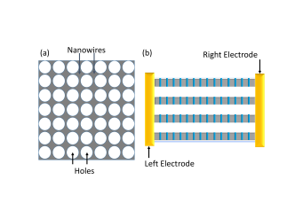
Here, we perform theoretical calculations of the thermoelectric properties of intrinsic SLNW connected with electrodes by using a linear chain of strongly coupled QDs. The electron carriers in SLNWs are provided by metallic electrodes with Fermi level below the conduction band minimum as proposed in[14]. The SLNW structure can be realized by starting with a superlattice with optimized period to minimize the phonon thermal conductance. The creation of nanowires may be achieved by lithographically drilling a periodic array of closely-spaced holes[10], leaving an array of nanowires (with a star-shaped cross-section) as depicted in Fig. 1. To reduce the electron scattering from the rough surface, the side surfaces of the nanowires are oxidized to form a high electron barrier, which serves the purpose of confining electrons in the the central region of the star-shaped nanowires. Due to the strong confinement of electrons, the electron-surface scattering can be reduced. At the same time the acoustic phonons are not so well confined in the central region which will then suffer more surface scattering. With such a design, we found that may be achieved in a thin SLNW with reasonable physical parameters adopted. Our theoretical studies should provide a useful guideline for the design of future thermoelectric devices operating at room temperature.
II Formalism
To model the thermoelectric properties of SLNWs, we consider a linear chain of strongly-coupled QDs with a system Hamiltonian given by an Anderson model ,[15] where
The first two terms of Eq. (1) describe the free electron gas in the left and right electrodes. () creates an electron of momentum and spin with energy in the left (right) electrode. () describes the coupling between the left (right) lead with its adjacent QD. () creates (destroys) an electron in the QD connected to the left (right) lead.
| (2) |
where is the QD energy level in the -th QD and describes the electron hopping strength between the -th and -th QDs. Here, for simplicity, we consider only one energy level for each QD, which is suitable for nanoscale QDs with no vally degeracy. For example, a cylidrical GaAs QD with high lateral potential barrier resulting from oxidation and vertical confinement via the band onset between GaAs and AlGaAs has a bound state (which is well separated in energy from the excited states) for diameter naer and height near .[16] For silicon QDs in the Si/Ge SLNW, we expect the valley degeneracy to lead to enhanced density of states in the energy range of interest, which can actually improve ZT further.[17] It should be noted that the Hubbard-like terms for Coulomb interactions between electrons in the SLNWs are neglected, since the electrons are delocalized along the transport direction in the strong hopping limit considered.
To study the transport properties of QDs junction connected with electrodes, it is convenient to use the Green-function technique. The electron and heat currents from reservoir to its adjacent QD are calculated according to the Meir-Wingreen formula[18]
where is for the electrical current and for the heat current. is the tunneling rate for electrons from the left (right) reservoir and entering the left (right) QD. denotes the Fermi distribution function for the -th electrode, where and are the chemical potential and the temperature of the electrode. , , and denote the electron charge, the Planck’s constant, and the Boltzmann constant, respectively. , , and denote the frequency-domain representations of the one-particle lessor, retarded, and advanced Green’s functions, respectively.
In the linear response regime electrical conductance (), Seebeck coefficient () and electron thermal conductance () can be evaluated by using Eq. (3) with a small applied bias and temperature difference across junction .[17] For simplicity, we calculate these thermoelectric coefficients in terms of Landauer formula[19,20]. Here we have , and . Thermoelectric coefficients are given by
| (4) |
where is the Fermi distribution function of electrodes at equilibrium temperature and is the transmission coefficient. is the Fermi energy of electrodes. The expression of in Eq. (4) is given by [20,21]
| (5) |
where denotes the one-particle retarded Green function of the leftmost QD with the energy level of , in which the self energy resulting from electron tunneling from the leftmost QD to the right electrode mediated by N-1 QDs is given by [21]
| (6) |
where denotes the total number of QDs. The rightmost QD is the th QD. The effective tunneling rate . For simplicity, we assume and for all and being the nearest neighbor of , and .
The figure of merit contains the phonon thermal conductance () of SLNW, which can not be neglected at room temperature.[17] Many theoretical efforts have been devoted to the study of phonon thermal conductance of silicon nanowires.[22,23] Here, we adopt the formula of phonon thermal conductance as given in Ref. [23], which can well describe the experimental results of Si nanowires.[23,24] We have
| (7) |
where is the phonon frequency and the throughput function. In [12,13,25] it is theoretically demonstrated that of Si nanowires filled with QDs is significantly reduced from the value for Si nanowires without QDs for a wide range of temperatures. To simulate the phonon thermal conductance of SLNWs (which is filled with QDs), we use a simple expression where is a dimensionless scaling factor used to describe the phonon scattering resulting from the interface scattering of QDs, a filtering mechanism for short wavelength acoustic phonons.[12,13] Values of can range from 0.1 to 1.[12,13,25] It is well known that QD size fluctuation and surface roughness will also degrade the electron transport[26,27] For simplicity, we assume that the electrical conductance and thermal conductance due to electron-phonon scattering and electron scattering from the surface roughness and QD size fluctuation can be modeled by a same scaling factor , where and denote the channel length and electron mean free path, respectively. Namely, the electrical conductance and thermal conductance for realistic SLNWs are expressed as and , respectively. The resulting now reads where . For an optimized design of SLNW as illustrated in Fig. 1, it is conceivable that can be less than 1. is roughly proportional to the ratio of mean-free path to the channel length. The mean-free path of electrons in germanium/silicon nanowires reported is beyond 170nm at room temperature.[27] Thus, for a micron size SLNW considered here, and the best value of can be expected is around 0.5. Taking the possible size nonuniformity of QDs into account, we shall consider the value of to be between 0.7 and 1 in our simulation and examine what values of can be achieved for SLNWs.
III Results and discussion
Before discussing the optimization of at room temperature, we first study the power factor () of SLNWs as a function of system parameters such as QD energy level (relative to ) and the tunneling rate (), since the behavior of is mostly determined by in the limit . Figure 2 shows the electrical conductance, Seebeck coefficient and power factor as functions of QD energy level () relative to the Fermi level () at two different temperatures. All energy scales are in units of , which is taken to be . In the strong-hopping limit, , the expression of can be approximated by
| (8) |
where for . At low temperature (), the behavior of can be roughly described by , which is nonzero only when falls within the SLNW band, which covers the range from -32 to 32, since the band width is . [See Fig. 2(a)] The spectrum becomes significantly broadened near room temperature with . The enhancement of outside the SLNW band is due to the thermionic effect.[14] As seen in Fig. 2(b), the Seebeck coefficient is an antisymmetric function of . Such a bipolar behavior has been reported in several studies.[19,21] The negative sign of indicates the main contribution coming from electrons tunnel through the resonant channels of the band above the Fermi level, while the positive sign of indicates the main contribution coming from holes tunneling through the band below . As seen in Fig. 2(c) the spectrum shows two strong peaks when is near the SLNW band edges at low temperature, and the peaks are broadened and shifted away from the band region as temperature increases.
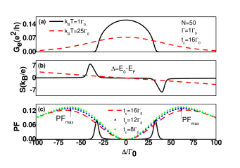
To find the maximum of at room temperature (), we also calculate as a function of for various coupling strengths. It is found that the maximum occurs near . Interestingly, this feature is nearly independent of the number of QDs in SLNW as long as is small.
Let’s consider the case of , which has an analytical solution. We have
| (9) |
Under the assumption of , we have
| (10) |
and
| (11) |
From Eqs. (10) and (11), we get which explains the linear behavior of at in Fig. 2(b). Furthermore,
| (12) |
where denotes the electron quantum conductance. The above equation gives a maximum at . This result holds well for any number of (tested up to ) as long as .
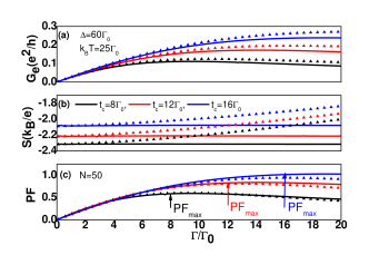
In Fig. 2, we have considered the case with . Next, we study how the thermoelectric properties of SLNW are affected by increasing the tunneling rate . Figure 3 shows the calculated , and as functions of for various values of at the optimum condition with . The dependence of is dominated by since is almost independent of as can be seen in Fig. 3(b). It is found that the maximum occurs when , as indicated by arrows in Fig. 3(c). We found this relation also holds approximately for any value of . For comparison, we also add the results obtained by Eq. (9) for (curves with triangle.[28]
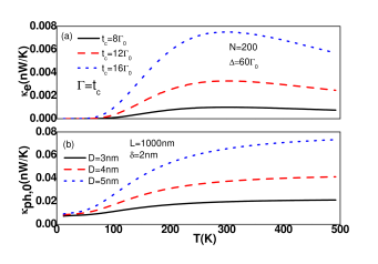
Although previous theoretical studies have predicted high values of QD junctions in the Coulomb blockade regime [19]for the case of , it is valid only at extremely low temperature. To illustrate the importance of , we show in Fig. 4 and as functions of temperature at and . As seen in Fig. 4(a) reaches a maximum at and the maximum value is enhanced with increasing or . Here we have adopted the optimum case with . For the Si/Ge superlattice with an optimized period of , the SLNW with has a length of . Therefore, we are interested in of nanowires with length of . The calculated based on Eq. 7 for silicon nanowires with surface roughness width and are shown in Fig. 4(b) for three different diameters (). The magnitude of is reduced very quickly when is reduced. We find that is larger than at even though for the . Both and will be included in the calculation of .
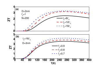
The calculated as a function of temperature for various values of is shown in Fig. 5. The optimum condition has been used. It is seen in Fig. 5(a) that can reach 3 at with even with . If we assume that phonons suffer more scattering from QDs than electrons (i.e. ) as implied in previous studies,[12,13,25] the resulting of SLNWs can be further enhanced as illustrated in Fig. 5(b) for . The value of can be larger than 3 over a wide temperature range. This feature can be very useful for the application of TEG at room temperature.
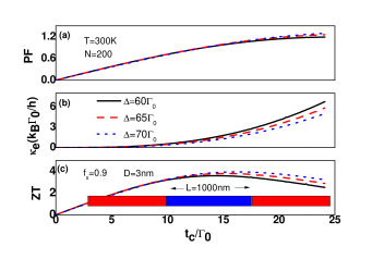
Finally, we examine the dependence of on the hopping strength, (which controls the SLNW band width) for a few values of around the optimum condition. The behaviors of , and for SLNWs as functions of (=) are shown in Fig. 6. It is found that reaches a maximum around , while both and continue to increase with increasing . The rate of increase for surpasses that for at , leading to an optimized condition for at that value. In Fig. 6(c), we found that for , the optimum condition for increases slightly with the best value occurring at . The main reason for the shift of optimum value of at large is due to the decrease of for increasing as seen in Fig. 6(b).
IV Conclusion
We have theoretically studied the thermoelectric properties of SLNWs connected to electrodes at room temperature. At higher temperatures (including room temperature) with much greater than and , we find the Seebeck coefficient can be approximately described by a linear relation and the maximum of the power factor occurs at . In addition, both the electrical conductance and power factor are maximized under the condition for fixed around . behavior is dominated by when . However, for large and , becomes significant and the maximum is determined not only by , but also by . All the above results are almost independent of the number of QDs in the SLNW. For thin Si/Ge SLNWs with diameter around , we find that it may be possible to achieve a larger 3 when the reduction of phonon thermal conductivity due to scattering from QDs is more severe than the reduction of electron conductivity. The linear chain model used here did not take into account the valley degeneracy and excited states of QDs. Adding these will provide more channels for electron conduction, which should improve further.[17] A realistic modeling taking into account the multi-valley band structures of Si and Ge will be left for future investigations.
Acknowledgments
This work was supported under Contract Nos. MOST 106-2112-M-008
-014 and MOST 104-2112-M-001-009 YM2.
E-mail address: mtkuo@ee.ncu.edu.tw
E-mail address: yiachang@gate.sinica.edu.tw
References
- (1) G. Chen, M. S. Dresselhaus, G. Dresselhaus, J. P. Fleurial and T. Caillat, International Materials Reviews, 48, 45 (2003).
- (2) A. J. Minnich, M. S. Dresselhaus, Z. F. Ren and G. Chen, Energy Environ Sci, 2, 466 (2009).
- (3) R. Venkatasubramanian, E. Siivola,T. Colpitts,B. O’Quinn, Nature 413, 597 (2001).
- (4) T. C. Harman, P. J. Taylor, M. P. Walsh, B. E. LaForge, Science 297, 2229 (2002).
- (5) F. Suarez, A. Nozariasbmarz, D. Vashaee and M. C. Ozturk, Energy Environ Sci, 9, 2099 (2016).
- (6) L. D. Hicks, and M. S. Dresselhaus, Phys. Rev. B 47, 16631 (1993).
- (7) N. Mingo, Appl. Phys. Lett.85, 5986 (2004).
- (8) A. I. Boukai, Y. Bunimovich, J. Tahir-Kheli, J. K. Yu, W. A. Goddard III and J. R. Heath, Nature, 451, 168 (2008).
- (9) A. I. Hochbaum1, R. K. Chen, R. D. Delgado, W. J. Liang, E. C. Garnett, M. Najarian, A. Majumdar, and P. D. Yang, Nature 451, 163 (2008).
- (10) J. H. Lee, J. W.Lim, and P. D. Yang, Nano Lett.15, 3273 (2015).
- (11) E. B. Ramayya, L. N. Maurer, A. H. Davoody, and I. Knezevic, Phy. Rev. B 86, 115328 (2012).
- (12) D. L. Nika, E. P. Pokatilov, A. A. Balandin, V. M. Fomin, A. Rastelli, and O. G. Schmidt, Phys. Rev. B 84, 165415 (2011).
- (13) Ming Hu and Dimos Poulikakos, Nano Lett. 12, 5487 (2012).
- (14) G. D. Mahan and L. M. Woods, Phys. Rev. Lett. 80, 4016 (1998).
- (15) H. Haug and A. P. Jauho, Quantum Kinetics in Transport and Optics of Semiconductors (Springer, Heidelberg, 1996).
- (16) D. M. T. Kuo, Y. C. Chang, Phys. Rev. B 89 (2014) 115416. 14
- (17) D. M. T. Kuo, C. C. Chen, and Y. C. Chang, Phys. Rev. B 95, 075432 (2017).
- (18) Y. Meir and N. S. Wingreen, Phys. Rev. Lett. 68, 2512(1992).
- (19) D. M.-T. Kuo and Y. C. Chang, Phys. Rev. B 81, 205321 (2010).
- (20) B. H. Teng, H. K. Sy, Z. C. Wang, Y. Q. Sun, and H. C. Yang, Phy. Rev. B 75, 012105 (2007).
- (21) D. M. T. Kuo and Y. C. Chang, J. Vac. Science and Technology, 31, 04D108 (2013).
- (22) P. G. Murphy and J. E. Moore, Phys. Rev. B 76, 155313 (2007).
- (23) R. K. Chen, A. I. Hochbaum, P. Murphy, J. Moore, P. D. Yang, and A. Majumdar, Phys. Rev. Lett. 101, 105501 (2008).
- (24) D. Li, Y. Y. Wu, P. Kim, L. Shi, P. D. Yang, and A. Majumdar, Appl. Phys. Lett. 83, 2934 (2003).
- (25) X. Mu, L. Wang, X. M. Yang, P. Zhang, A. C. To, T. F. Luo, , Scientific Reports 5 16697 (2015).
- (26) D. M. T. Kuo and Y. C. Chang, Nanotechnology 24, 175403 (2013).