Comparison of Sensitivity and Low Frequency Noise Contributions in GMR and TMR Spin Valve Sensors with a Vortex State Free Layer
Abstract
Magnetoresistive spin valve sensors based on the giant- (GMR) and tunnelling- (TMR) magnetoresisitve effect with a flux-closed vortex state free layer design are compared by means of sensitivity and low frequency noise. The vortex state free layer enables high saturation fields with negligible hysteresis, making it attractive for applications with a high dynamic range. The measured GMR devices comprise lower pink noise and better linearity in resistance but are less sensitive to external magnetic fields than TMR sensors. The results show a comparable detectivity at low frequencies and a better performance of the TMR minimum detectable field at frequencies in the white noise limit.
I Introduction
Magnetoresistive sensors have a great significance in industry. They are utilized in a vast spectrum of applications such as compass-, biomedical-, automotive- and aerospace applications Luong et al. (2017); Valadeiro et al. (2017); Scherner and Slatter (2014); Hartmann (2011).
The most prominent sensor design is the spin valve principle with a basic common structure of two adjacent magnetic layers separated by a spacer layer.
One magnetic layer has a pinned magnetisation (further referred to as pinned layer) whereas the other one changes its total magnetisation in external magnetic fields (further referred to as free layer). The electric resistance depends on the relative angle of magnetisation between the magnetic layers.
Recently, a new sensor concept with a circular shaped free layer was suggested Zimmer et al. (2015). Due to the shape, material properties and a certain relation of thickness to diameter a flux-closed vortex magnetisation state forms when small or no external fields are applied.
Magnetoresistive spin valve sensors operated in a magnetic vortex configuration show negligible hysteresis while saturating at high magnetic field Wurft et al. (2017).
These properties make them very attractive for linear current sensors or position sensors with the need for a high dynamic range and accuracy, since the latter is limited by hysteresis Xie et al. (2017); Windl et al. (2017).
Other examples are wheel speed or angle sensing applications Granig et al. (2007); Kapser et al. (2008) where this principle could facilitate the mechanical adjustment as well as enabling more freedom setting the working point.
This paper focuses on the comparison of giant magnetoresistive (GMR) and tunnelling magnetoresistive (TMR) devices exploiting the vortex free layer design.
The devices consist of a similar element arrangement and magnetic layer properties to study the sensitivity and low frequency noise. These parameters are determining the detectivity, a frequency dependent parameter giving the minimum detectable field to compare the measured devices.
II Theoretical Model
II.1 Noise Model
Thermal noise is present in any dissipative structure arising from the random motions of the charge carriers Vasilescu (2006). The thermal noise term can be described as frequency independent voltage noise power with the Nyquist formula containing the temperature in Kelvin, Boltzmann’s constant and the total resistance :
| (1) |
As soon as a DC current is applied on a resistive medium, -noise, also known as pink noise, arises Vasilescu (2006); Hooge (1994); Dhagat et al. (2005); Jiang et al. (2004). In case of a magnetoresistive (MR) element, pink noise is described as the result of interactions from the charge carriers with defects and domain fluctuations in the magnetic layers. The pink noise term decreases with the frequency and is proportional to the squared current :
| (2) |
This noise arises from a statistical process, meaning the factor from (2) is decreasing with increasing sensor area Lei et al. (2011); Nor and Hill (2002); Smith et al. (1996); Egelhoff et al. (2009); Reed et al. (2001). Therefore it can be splitted into , with being the area of one sensitive element and N the number of elements connected in series. Since both noise parts are arising from different physical processes and are therefore uncorrelated, the contributions can be summed up to the total frequency dependent noise power for the theoretical description of the GMR sensor:
| (3) | |||||
| (4) |
In case of a biased TMR sensor an additional shot noise term has to be taken into account. Shot noise arises because the charge carriers are quantised at a potential barrier, leading to random arrival times Boggs et al. (1995); Vasilescu (2006). The thermal assisted barrier crossing is therefore superimposed by a field-assisted barrier crossing of the charge carriers Klaassen et al. (2004). It is commonly expressed as a combination of Nyquist- and shot noise Nowak et al. (1999); Egelhoff et al. (2009); Ishihara et al. (2001) giving the total noise of magnetic tunnel junctions (MTJ) connected in series:
| (5) |
The first term results in Nyquist formula if or full shot noise of for the case , taking into account the serially connected devices Nowak et al. (1999); Guerrero et al. (2009); Egelhoff et al. (2009). This term may not be suitable for all TMR structures and therefore a Fano factor is often introduced Lei et al. (2011) to compensate deviations. Due to frequency limitations of the measurements to , the shot noise limit is not visible. Therefore the validity of equation (5) is assumed for all TMR noise calculations.
II.2 Transfer Curve and Sensitivity
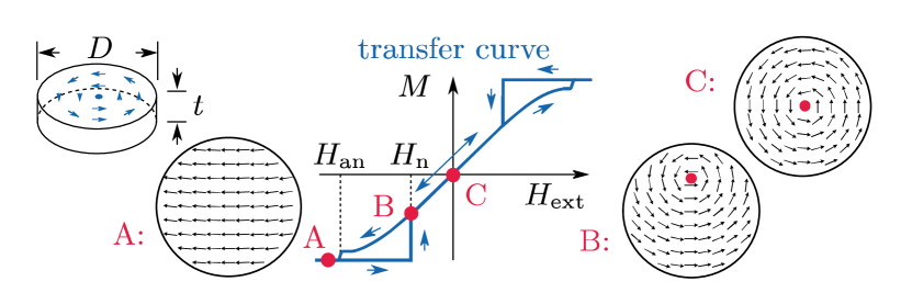
In contrast to anisotropy pinned free layer designs, the transfer curve of vortex-state free layer sensors is characterized by a nucleation () and annihilation () field (see Fig. 1).
Annihilation arises from the extinction of the vortex core in strong magnetic fields to increase the average magnetisation component towards the external field, stabilizing in a single domain state.
This is the sensors saturation state, present until the external field decreases to the nucleation field where a stable vortex magnetisation with negligible hysteresis is formed.
The hysteretic behaviour between nucleation and annihilation point as well as its dependence on the material properties is studied in detail by Wurft et al. Wurft et al. (2017) using micromagnetic simulations.
The analytical “rigid” vortex model, extensively described in Guslienko et al. (2001a, b); Guslienko (2008), assumes a fixed circular vortex spin structure which shifts in respect to the disc center when magnetic fields are applied.
This shift of the vortex core leads to an increasing area where the magnetisation of the free layer is either parallel or antiparallel to the magnetisation of the pinned layer, depending on the direction of the external field.
The movement of the vortex center as a response to external magnetic fields is isotropic for the lateral dimensions Guslienko et al. (2001a), but in this context external applied fields are aligned parallel or antiparallel with the magnetisation of the pinned layer.
The MR effect is defined in spin valve systems as
| (6) |
The sensitivity is related to the magnetic stiffness of the free layer, dependent on the aspect ratio with the thickness and the diameter of the vortex state free layer. The normalised sensitivity is calculated by the derivative of the resistance or conductance with respect to the change in applied field strength:
| (7) |
is the resistance and the conductance of the sensor at zero external field.
In TMR devices, the conductance is in first order linear with the cosine of the relative angle between the pinned and free layer magnetisations.
The detectivity describes the minimum detectable field Guerrero et al. (2009); Stutzke et al. (2005) and is given as the sensors voltage noise divided by the voltage dependent sensitivity. It is commonly used to compare different sensors:
| (8) |
III Sample Preparation and Measurement Set-Up
The pinned layers consist of a physical vapour deposited (PVD) antiferromagnetically coupled CoFe/Ru/CoFe stack with a PtMn pinning layer. In case of GMR, copper is used as spacer layer, TMR has a MgO barrier instead.
In both cases the free layer has a cylindrical shape pattered by photolithography and ion beam etching.
It has a thickness of and is made of a cobalt-iron based alloy.
All samples consist of an array with ten elements connected in series.
In GMR the current is in plane with the element contacted at the bottom.
In TMR the current is perpendicular to plane with the contacts above and below the magnetic layers.
The resistance measurements were performed in a calibrated electromagnet.
For the noise measurements the DUT is supplied by a battery.
An ultra low noise amplifier Scandurra et al. (2011) is used with a lock-in amplifier to obtain the frequency resolved noise amplitudes.
To avoid destruction through Joule heating or a breakdown of the barrier, the sensors were biased with not more than () in case of GMR or a junction voltage of for TMR respectively.
IV Measurements and Results
IV.1 Field Measurements
| D | RAP | MR | ||||
| [] | [] | [] | [] | [] | ||
| TMR | 2 | 5750 | 4805 | 85 | ||
| TMR | 1 | 26500 | 21633 | 73 | ||
| GMR | 2 | 71.5 | 70.1 | 4.3 | ||
| GMR | 1 | 68.2 | 66.9 | 3.9 |
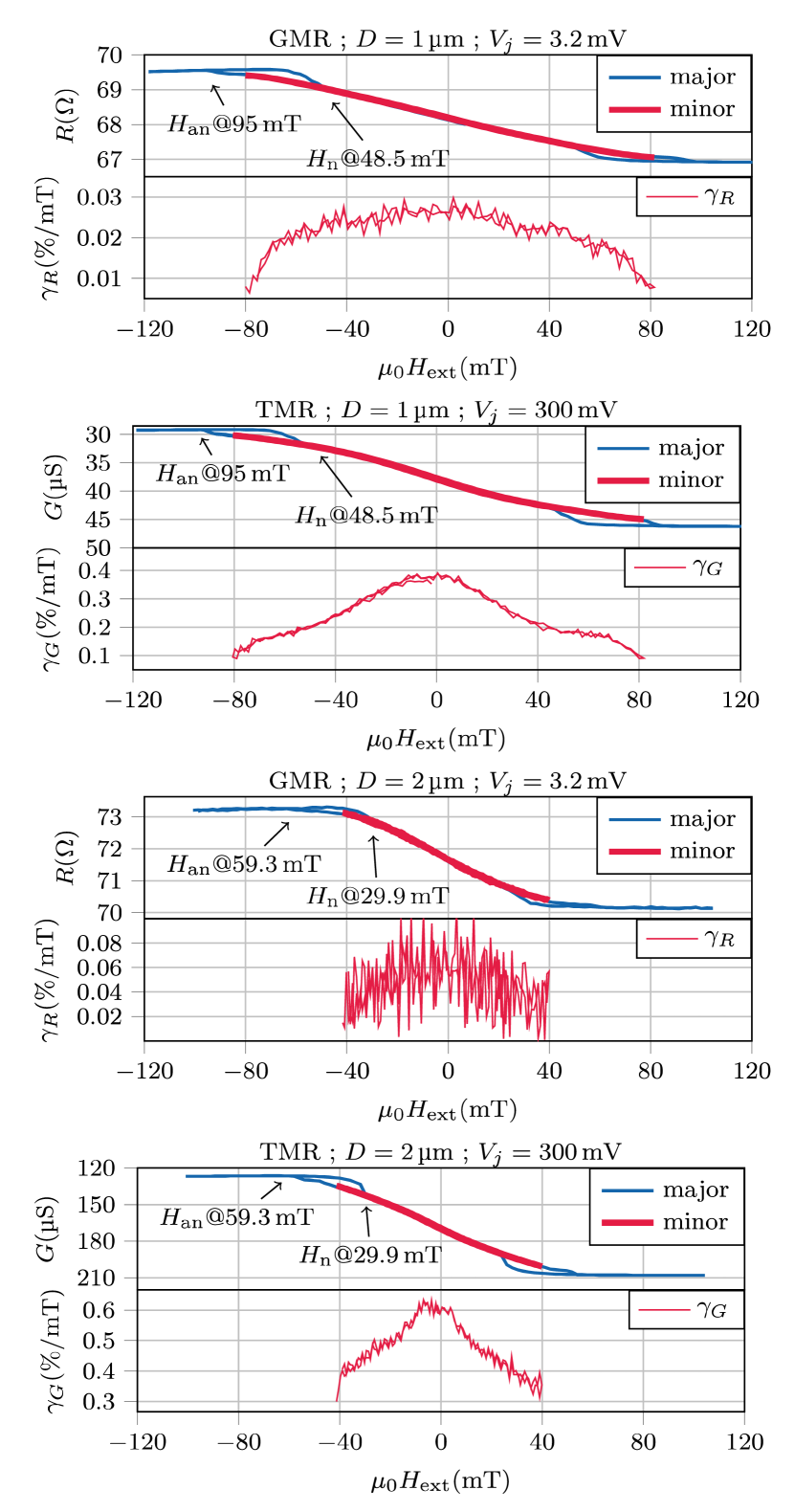
TMR and GMR samples with different free layer diameters have been investigated.
The resistance parameters are given in Table 1, the transfer characteristic for all sensors are shown in Figure 2.
Hysteresis is only present if the annihilation field of the vortex core is reached and a single domain state of the free layer is forming (Figure 2 major loops).
If the vortex is present, i.e. the field remains smaller than the annihilation field, hysteresis is negligible (Figure 2 minor loops).
The “rigid” vortex model predicts a decreasing sensitivity with increasing aspect-ratio .
As can be seen in the measurements, a doubling of the diameter decreases , and therefore, increases the sensitivity .
IV.2 Noise Measurements
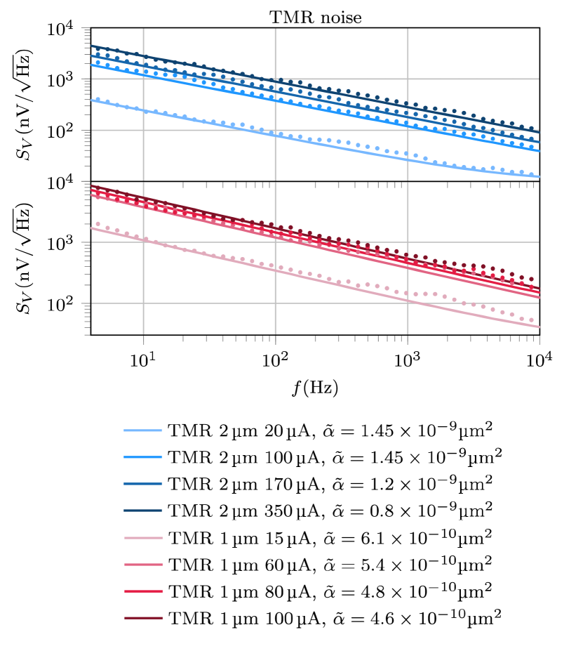
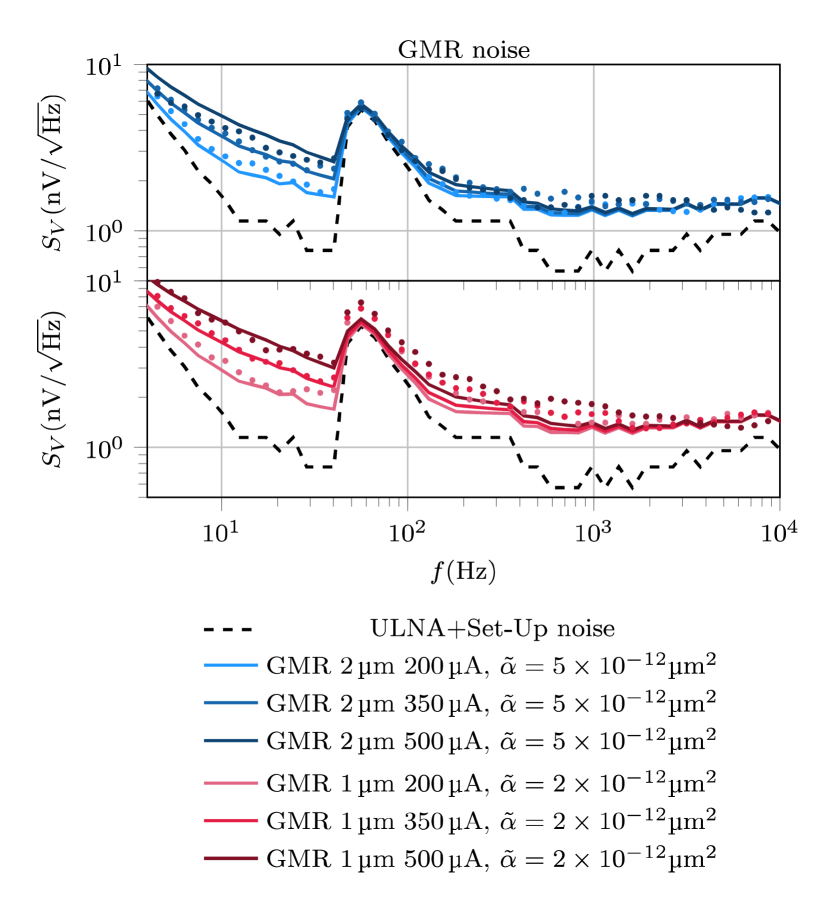
The frequency dependent noise measurements are shown in Figure 3 and 4 for devices with and free layer diameter.
The measured signal is clearly above the noise floor of the ULNA and induced disturbances (black dashed lines in Fig. 4).
The theoretical curves (colored lines) are fitted to the measurements (dots) with equations (4) and (5) for GMR and TMR sensors, respectively.
The fit includes the amplifier noise, the thermal and shot noise level as well as the pink noise with the empirical noise parameter , which is the only fit parameter.
Bumps observed in the TMR noise spectra, leading to a deviation of the fit curves to the measurement, may be attributed to random telegraph noise (RTN) as also reported in Almeida et al. (2008).
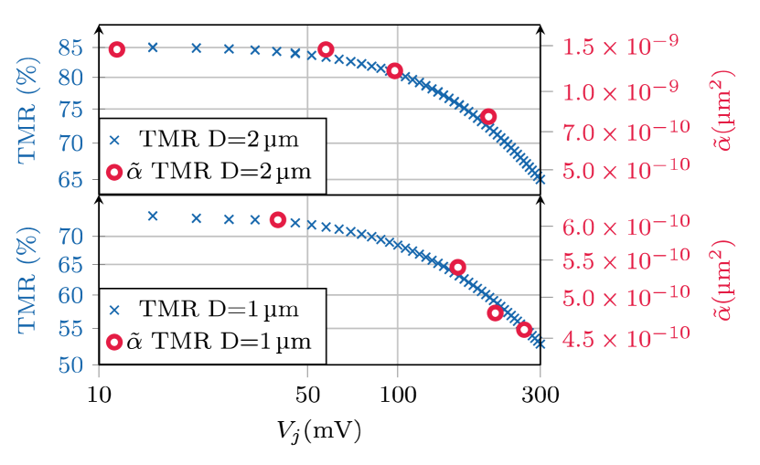
As extracted from the fitted curves, the TMR samples exhibit a noise parameter higher by a factor of 300 compared to the GMR samples.
The high pink noise contribution in TMR is shifting the corner frequency (between and white noise floor) out of the measurement range.
Therefore only pink noise contributions are visible.
Although the noise parameter is normalised to the sensors area, it is roughly a factor of two between diameter of and for both GMR and TMR devices.
This is attributed to the magnetic stiffness of the free layer, increasing with the parameter as can also be seen in the annihilation field .
As the TMR is decreasing with higher supply voltage, the noise parameter is reduced as well.
This behaviour of the noise parameter is also discussed in Almeida et al. (2008); Han et al. (2010).
Figure 5 shows the bias voltage dependence of the TMR and .
Trends for the correlation of the noise parameter with the resistance area product and the TMR effect are given in Lei et al. (2011) and Gokce et al. (2006). The values from the literature are in good agreement with the measurements.
As this effect is not present in GMR sensors, the noise parameter is constant.
IV.3 Detectivity Comparison
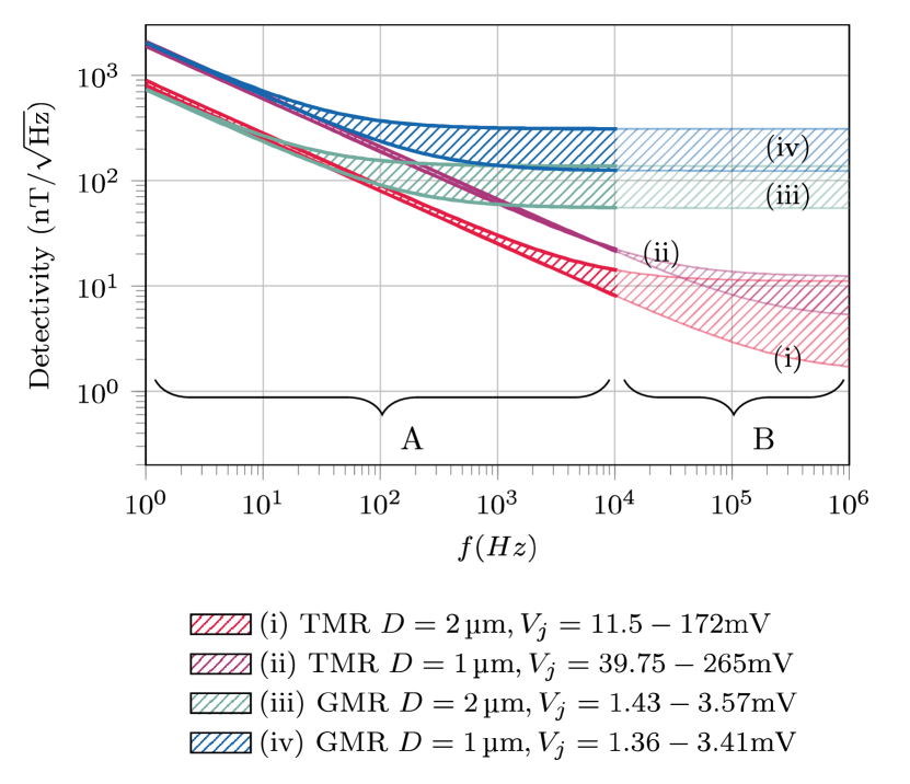
The detectivity comparison is shown in Figure 6.
It is calculated using equation (8) with the obtained parameters from the fitted noise data in Figures 3 and 4.
The plotted areas indicate the detectivity obtained from the measured array configuration of 10 serially connected devices, considering all applicable supply voltages as described in section III.
The plot is divided into region A, where the detectivity is obtained from the fitted noise measurements, and region B, an extrapolation using the formulas (4) and (5) for white and pink noise contributions.
A higher supply voltage is generally improving the detectivity in the high frequency regime for GMR and TMR sensors, as also observed in literature Reig et al. (2013).
The detectivity in this regime is proportional to the sensitivity which is improved at a larger bias.
But since the TMR effect as well as the sensitivity and noise parameter of the TMR are decreasing with the supply voltage, the shapes differ to areas obtained by the GMR sensors.
The same free layer diameter leads to roughly the same detectivity level in the low frequency range where flicker noise is dominant.
Even though the noise parameter , the TMR sensor has the same detection limit in the low frequency regime and clearly wins in the high frequency regime considering white and pink noise contributions.
The TMR sensors have a better detectivity performance at higher frequencies due to the better sensitivity while having only a 1.5 times larger noise floor when considering shot and thermal noise contributions as given in equation (5).
The low frequency detectivity is roughly on the same level for GMR and TMR sensors with the same area.
At , as the white noise becomes dominant, the curves are splitting up. The knee between pink and white noise contributions is dependent on design parameters like resistance, area or bias voltage.
For practical applications, the corner frequency can be at or even higher Stutzke et al. (2005).
One possible interpretation for the dependence of the low frequency detectivity on the sensors area is a magnetic origin of the pink noise as also stated in Ozbay et al. (2006).
A derivation by Egelhoff et al. Egelhoff et al. (2009) for MTJ‘s shows the independence of the detectivity on the magnetoresistive effect and bias voltage for pink magnetic noise.
V Conclusion and Outlook
In this work giant- and tunnelling magnetoresistive spin valve sensors with a magnetic vortex state free layer disk were compared. All samples were based on the same free layer thickness, free layer material and had the same amount of active elements or junctions connected in series, leading to comparable sensor properties. The broad linear range is given by the annihilation field of the magnetic vortex state, dependent on the ratio of thickness to diameter. Compared to the GMR sensors, the noise parameter of the TMR sensors is 300 times higher. Yet the TMR sensors show a lower detection limit at frequencies where white noise is dominant. This is attributed to the high TMR sensitivity. The detectivity can be improved by using higher supply voltages, despite the fact of a thereby decreasing sensitivity in TMR sensors. The same free layer diameter leads to roughly the same detectivity level in the low frequency range where for GMR as well as TMR sensors pink noise is dominant. This suggests that the noise in the low frequency regime is dominated by magnetic contributions, because magnetic pink noise is not dependent on the MR effect or the bias voltage but on the active sensor area. The next-stage work will be a study on segregated electric and magnetic noise contributions in vortex-state free layer devices.
VI Acknowledgements
The authors would like to gratefully acknowledge the Christian Doppler Laboratory Advanced Magnetic Sensing and Materials, for financial support. The Laboratory is financed by the Austrian Federal Ministry of Economy, Family and Youth, the National Foundation for Research, Technology and Development.
References
- Luong et al. (2017) V. S. Luong, Y. H. Su, C. C. Lu, J. T. Jeng, J. H. Hsu, M. H. Liao, J. C. Wu, M. H. Lai, and C. R. Chang, IEEE Transactions on Nanotechnology PP, 1 (2017).
- Valadeiro et al. (2017) J. Valadeiro, M. Silva, S. Cardoso, M. Martins, J. Gaspar, P. P. Freitas, and A. M. Sebastião, in 2017 IEEE Sensors Applications Symposium (SAS) (2017) pp. 1–6.
- Scherner and Slatter (2014) S. Scherner and R. Slatter, in CIPS 2014; 8th International Conference on Integrated Power Electronics Systems (2014) pp. 1–7.
- Hartmann (2011) M. Hartmann, Ultra-compact and ultra-efficient three-phase PWM rectifier systems for more electric aircraft, Ph.D. thesis, ETH Zurich (2011).
- Zimmer et al. (2015) J. Zimmer, A. Satz, W. Raberg, H. Brueckl, and D. Suess, “Device, magnetic sensor device and method,” (2015), uS Patent App. 14/141,660.
- Wurft et al. (2017) T. Wurft, W. Raberg, K. Pruegl, A. Satz, G. Reiss, and H. Brueckl, IEEE Transactions on Magnetics PP, 1 (2017).
- Xie et al. (2017) F. Xie, R. Weiss, and R. Weigel, IEEE Transactions on Industrial Electronics 64, 710 (2017).
- Windl et al. (2017) R. Windl, C. Abert, F. Bruckner, C. Huber, C. Vogler, H. Weitensfelder, and D. Suess, AIP Advances 7, 115121 (2017), https://doi.org/10.1063/1.5004499 .
- Granig et al. (2007) W. Granig, S. Hartmann, and B. Koeppl, in SAE Technical Paper (SAE International, 2007).
- Kapser et al. (2008) K. Kapser, S. Zaruba, P. Slama, and E. Katzmaier, “Advanced microsystems for automotive applications 2008,” (Springer, Berlin, Heidelberg, 2008) Chap. Speed Sensors for Automotive Applications Based on Integrated GMR Technology.
- Vasilescu (2006) G. Vasilescu, Electronic Noise and Interfering Signals: Principles and Applications, Signals and Communication Technology (Springer Berlin Heidelberg, 2006).
- Hooge (1994) F. N. Hooge, IEEE Transactions on Electron Devices 41, 1926 (1994).
- Dhagat et al. (2005) P. Dhagat, A. Jander, and C. A. Nordman, Journal of Applied Physics 97, 10C911 (2005), http://dx.doi.org/10.1063/1.1851952 .
- Jiang et al. (2004) L. Jiang, E. Nowak, P. Scott, J. Johnson, J. Slaughter, J. Sun, and R. Dave, Physical Review B - Condensed Matter and Materials Physics 69, 544071 (2004), cited By 88.
- Lei et al. (2011) Z. Q. Lei, G. J. Li, W. F. Egelhoff, P. T. Lai, and P. W. T. Pong, IEEE Transactions on Magnetics 47, 602 (2011).
- Nor and Hill (2002) A. F. M. Nor and E. W. Hill, IEEE Transactions on Magnetics 38, 2697 (2002).
- Smith et al. (1996) N. Smith, A. M. Zeltser, and M. R. Parker, IEEE Transactions on Magnetics 32, 135 (1996).
- Egelhoff et al. (2009) W. Egelhoff, P. Pong, J. Unguris, R. McMichael, E. Nowak, A. Edelstein, J. Burnette, and G. Fischer, Sensors and Actuators A: Physical 155, 217 (2009).
- Reed et al. (2001) D. S. Reed, C. Nordman, and J. M. Daughton, IEEE Transactions on Magnetics 37, 2028 (2001).
- Boggs et al. (1995) C. K. Boggs, A. D. Doak, and F. L. Walls, in Proceedings of the 1995 IEEE International Frequency Control Symposium (49th Annual Symposium) (1995) pp. 367–373.
- Klaassen et al. (2004) K. B. Klaassen, X. Xing, and J. C. L. van Peppen, IEEE Transactions on Magnetics 40, 195 (2004).
- Nowak et al. (1999) E. R. Nowak, M. B. Weissman, and S. S. P. Parkin, Applied Physics Letters 74, 600 (1999).
- Ishihara et al. (2001) K. Ishihara, M. Nakada, E. Fukami, K. Nagahara, H. Honjo, and K. Ohashi, IEEE Transactions on Magnetics 37, 1687 (2001).
- Guerrero et al. (2009) R. Guerrero, M. Pannetier-Lecoeur, C. Fermon, S. Cardoso, R. Ferreira, and P. P. Freitas, Journal of Applied Physics 105, 113922 (2009).
- Guslienko et al. (2001a) K. Y. Guslienko, V. Novosad, Y. Otani, H. Shima, and K. Fukamichi, Physical Review B 65 (2001a), 10.1103/PhysRevB.65.024414.
- Guslienko et al. (2001b) K. Y. Guslienko, V. Novosad, Y. Otani, H. Shima, and K. Fukamichi, Applied Physics Letters 78, 3848 (2001b).
- Guslienko (2008) K. Y. Guslienko, Journal of nanoscience and nanotechnology 8 6, 2745 (2008).
- Stutzke et al. (2005) N. A. Stutzke, S. E. Russek, D. P. Pappas, and M. Tondra, Journal of Applied Physics 97 (2005), 10.1063/1.1861375.
- Scandurra et al. (2011) G. Scandurra, G. Cannat, and C. Ciofi, AIP Advances 1 (2011), 10.1063/1.3605716.
- Almeida et al. (2008) J. M. Almeida, P. Wisniowski, and P. P. Freitas, IEEE Transactions on Magnetics 44, 2569 (2008).
- Han et al. (2010) G. C. Han, B. Y. Zong, P. Luo, and C. C. Wang, Journal of Applied Physics 107, 09C706 (2010), https://doi.org/10.1063/1.3357332 .
- Gokce et al. (2006) A. Gokce, E. R. Nowak, S. H. Yang, and S. S. P. Parkin, Journal of Applied Physics 99, 08A906 (2006).
- Reig et al. (2013) C. Reig, S. Cardoso, and S. C. Mukhopadhyay, Giant Magnetoresistance (GMR) Sensors: From Basis to State-of-the-Art Applications (Springer-Verlag Berlin Heidelberg, 2013).
- Ozbay et al. (2006) A. Ozbay, E. R. Nowak, A. S. Edelstein, G. A. Fischer, C. A. Nordman, and S. F. Cheng, IEEE Transactions on Magnetics 42, 3306 (2006).