Nanometer resolution mask lithography with matter waves: Near-field binary holography
Abstract
Mask-based pattern generation is a crucial step in microchip production. The next-generation extreme-ultraviolet- (EUV) lithography instruments with a wavelength of is currently under development. In principle, this should allow patterning down to a resolution of a few nanometers in a single exposure. However, there are many technical challenges, including those due to the very high energy of the photons. Lithography with metastable atoms has been suggested as a cost-effective, less-complex alternative to EUV lithography. The great advantage of atom lithography is that the kinetic energy of an atom is much smaller than that of a photon for a given wavelength. However, up till now no method has been available for making masks for atom lithography that can produce arbitrary, high resolution patterns. Here we present a solution to this problem. First, traditional binary holography is extended to near-field binary holography, based on Fresnel diffraction. By this technique, we demonstrate that it is possible to make masks that can generate arbitrary patterns in a plane in the near field (from the mask) with a resolution down to the nanometer range using a state of the art metastable helium source. We compare the flux of this source to that of an established EUV source (ASML, NXE:3100) and show that patterns can potentially be produced at comparable speeds. Finally, we present an extension of the grid-based holography method for a grid of hexagonally shaped subcells. Our method can be used with any beam that can be modeled as a scalar wave, including other matter-wave beams such as helium ions, electrons or acoustic waves.
I Introduction
In standard photolithography, the resolution is determined by the wavelength of the light: the smaller the wavelength, the higher the resolution. The present industrial photolithography standard is the immersion scanner using a light source. Following standard diffraction theory (Abbe resolution criterion) this light source gives a maximum resolution in air of . This is increased by use of off-axis illumination and a highly refractive immersion medium ITR (2015). Furthermore, in modern chip production the patterns are generated by subtle use of underexposure, overdevelopment, and multiple exposures so that patterns with a resolution of around can be created. Lithography methods for higher resolution exist; for example, electron-beam lithography, which is used to make the masks for photolithography. However, these are all serial lithography techniques and are much slower than mask-based lithography. The industry is currently implementing the next generation of lithography devices, and extreme-ultraviolet (EUV) lithography based on a -wavelength light source is expected to be able to produce patterns with a resolution of less than in single exposures ITR (2015).
Atom lithography has been suggested as an alternative to EUV lithography. For a given wavelength the energy of the atom is much less than the energy of the photon. For instance, the energy of an EUV photon of wavelength is , where denotes Planck’s constant and is the speed of light in a vacuum. On the other hand, a helium atom of the same wavelength () has a kinetic energy , where is the mass of the helium atom. High-intensity atom beams with narrow velocity distributions can be created by expansion from a high-pressure reservoir through a nozzle followed by selection of the central beam with a conically shaped aperture, which prevents backstreaming into the beam. This aperture is typically referred to as the “skimmer” Pauly (2000). For helium atoms with kinetic energies between (corresponding to a liquid-nitrogen-cooled beam) and (room-temperature beam), the corresponding wavelengths are between and . This makes atom beams, in principle, a very attractive candidate for high-resolution pattern generation. One approach in atom lithography is to use a beam of metastable atoms for the pattern generation. When a metastable atom hits the substrate, it decays, and the energy of the metastable state is transferred to the substrate Berggren et al. (1995); Baldwin (2005); Ueberholz et al. (2002). In their seminal paper from 1995, Berggren et al. Berggren et al. (1995) demonstrated pattern generation in a thiol-based resist using a beam of metastable argon atoms manipulated by a light-field mask. Since then numerous groups have experimented with atom lithography using either metastable noble-gas atoms and patterning in resist or direct deposition of atoms on substrates. The energy released when a metastable atom decays is about for argon and for helium Colli (1954); Baldwin (2005).
In most of these experiments the atomic beams were manipulated either by light or electrostatic fields Berggren et al. (1995); Gardner et al. (2017); Adams et al. (1994); Hinderthür et al. (1998). The reason for this is that atoms at low energies, as they typically are in these beams, do not penetrate any substrates. Furthermore the metastable atoms decay when they impinge on a surface. Therefore it is not possible to use masks made on substrates as is done in photolithography. The pattern has to be generated by open areas in the substrate where the beam can go through, so any closed path (i.e. a circle) would lead to the segment of the mask bounded by the closed path falling out. This limited the patterns that could be made in a mask configuration to essentially stripes and dots. Experiments have also been done that involve focusing of atom beams with lenses Eder et al. (2017); Koch et al. (2008); Doak et al. (1999); Carnal et al. (1991); Eder et al. (2015, 2012); Patton et al. (2006); Barr et al. (2016); Reisinger and Holst (2008). This can be used for serial writing of arbitrary patterns. However, for mass-scale production serial writing is not a suitable method.
In 1996 Fujita et al. Fujita et al. (1996) used a different approach. Instead of using light or electrostatic fields, they made a solid mask consisting of a distribution of uniformly sized holes, etched in a silicon nitride membrane. The hole distribution was calculated with the theory of grid-based binary holography developed by Lohmann and Paris Lohmann and Paris (1967), and later by Onoe and Kaneko Onoe and Kaneko (1979): grid-based binary holography imposes the limitation on the binary holograms that the openings are all of the same size and positioned at specific positions of a rectangular grid. That is to say, the holes are not only uniformly sized, but are also placed at a regular minimum spacing. The hole distribution is an approximated Fourier transform of the final, desired pattern. Murphy and Gallagher Murphy and Gallagher (1982) extended the binary-holography technique of Lohmann and Paris Lohmann and Paris (1967) to work also for hexagonal grids. Originally, the binary-holography method was developed to create holograms for electromagnetic waves with use of a computer, and the procedure is often referred to as “computer-generated holography” in the literature. Because of the de Broglie wavelength associated with a matter wave, the method also works for atom beams. It may be necessary to include a correction caused by the van der Waal interaction between the mask material and the atoms. However, as shown in a range of experiments Grisenti et al. (1999) the only effect will be a slightly smaller effective hole size, which can easily be corrected for. Thus, we do not discuss this further in this paper.
Because the phase of the atoms when they arrive at the image plane (target plane) is not important, only the intensity is, many different hole distributions can create the same intensity pattern. In a recent publication it was shown how it is possible to vary the number of open holes in a mask over a large range without changing the final pattern Nesse et al. (2017a). Coverage differences of up to were demonstrated.
Until now one major problem with the binary-holography method has been that it is based on monochromatic, plane incident and outgoing waves. The binary mask is generated on the basis of a Fourier transform of the target pattern, which is assumed to be located at infinity. This means that the standard binary-holography method cannot be used to make patterns with high spatial resolution without the introduction of a lens that draws the Fraunhofer diffraction pattern in from infinity. Some work has been done on atomic lenses as mentioned earlier but no lenses with the required precision presently exist. Furthermore real atom sources are not perfectly plane waves and they are not perfectly monochromatic. The monochromaticity and spatial coherence of an atom beam are determined by the velocity distribution (wavelength distribution) and extension of the source Patton et al. (2006). The ultimate coherent beam would seem to be a Bose-Einstein condensate (BEC). Recently, Keller et al. Keller et al. (2014) generated a beam of BEC metastable helium atoms. However, standard Fraunhofer diffraction theory does not apply for a BEC Fouda et al. (2016). Furthermore, the de Broglie wavelength of a dropping BEC of helium is very large, about after a drop of . For high-resolution lithography, one wants to use short wavelengths, since the wavelength determines the ultimate target pattern resolution that can be achieved. One can think of experimental ways to get around this (e.g., by moving the mask relative to the BEC so that the BEC wavelength relative to the mask becomes smaller) but considerable amendments would have to be made to the theory we present here. It is also very challenging to make a high-flux BEC source. It should be mentioned, however, that considerable progress has been made in this field in recent years Bolpasi et al. (2014); Bennetts et al. (2017).
Recently, a beam of metastable helium atoms with a very narrow wavelength distribution was produced with a pulsed source Even (2015). In this paper we show that it is possible to make binary masks that can be used to create patterns with nanometer resolution in a target plane close to the mask with use of an atom source with the wavelength distribution given above and no lenses.
The rest of this paper is organized as follows. Section II presents the theoretical background of the method that we use for the creation of the mask producing the desired pattern on the screen behind the mask. In particular, the method consists of an approximate backpropagation step based on Fresnel diffraction for plane waves (Sec. II.1), the mask-generation step using binary holography on hexagonal (or rectangular) lattices (Sec. II.2), and an evaluation step where our mask design is put to the test by application of rigorous forward-propagation techniques for the propagation of the field of realistic sources through the mask and onto the screen (Sec. II.3). The results obtained by this approach are presented and discussed in Sec. III. Section IV contains a discussion of the throughput of helium atoms that can be expected for realistic experimental parameters. In particular, we estimate the writing speed (throughput) that can be achieved with a state-of-the-art metastable-atom source and compare it with that of an established EUV source (NXE:3300, ASML). Finally, the conclusions that we draw from the study are presented in Sec. V. The Appendix details the binary-holography technique applied together with hexagonal grids.
II Theory
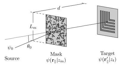
The lithography system that we consider is presented in Fig. 1. It consists of a source, a mask that will diffract the incident wave propagating from the source, and a target plane (or screen) where the diffraction pattern will be displayed. In Fig. 1, these elements of the setup are labeled “source”, “mask” and “target”, respectively. It is assumed that the mask and the target planes are parallel. In lithography one aims at creating in the target plane, typically with high resolution, a predefined pattern — called the “target pattern” in the following. We assume that such a target pattern has been identified and we stress that this pattern, in principle, can be arbitrary. However, in the target plane in Fig. 1, for the purpose of illustration, we use a structure consisting of a series of slightly displaced L shapes. This pattern is one of the standard resolution test patterns used in lithography Chang et al. (2001).
After the target pattern is chosen, the first step in the process of creating a binary holographic mask that corresponds to it consists in calculating the field just behind the mask plane (seen relative to the source). This field is referred to as the “mask field” in the following. It has the property that when this field is propagated to the target plane and the corresponding intensity is calculated, the target pattern is obtained (shown on the right in Fig. 1). To calculate the mask field, one therefore has to backpropagate the field from the target plane to the mask plane. The field in the target plane — the target field — is taken as the square root of the intensity distribution of the target pattern multiplied by an arbitrarily chosen phase function that can vary over this plane. By changing the phase function, one obtains different masks that in principle should give rise to the same intensity distribution of the target pattern. The backpropagation of the target field can be performed in a number of different ways; which approach is the most appropriate depends on the structure of the target pattern and the separation between the mask and target planes (indicated as in Fig. 1). Here our goal is to create high-resolution masks (less than ) that can be used in realistic lithographic setups based on neutral-atom beams. We therefore focus on geometries for which the source, mask, and screen (the target plane) are relatively close together;that is, the total (linear) system dimension is less than . Under this assumption, the backpropagation can be performed with the use of (near-field) Fresnel propagation Goodman (2005). For our purpose of generating high-resolution patterns, one cannot, for instance, rely on (far-field) Fraunhofer propagation Goodman (2005) which is used in existing binary-holography techniques. Therefore, to build a binary-holography technique around Fresnel propagation is novel and its use is prompted by the requirement of obtaining high resolution. The technique that is proposed here is called “near-field binary holography” in order to distinguish it from “standard” binary holography, which assumes the target plane is in the far-field.
In the second step of the design process, the calculated mask field is used as the starting point for generation of the mask. The structure of the mask is designed so that when an incident field, originating at the source, passes through it, the field just behind the mask approximately equals the mask field calculated during the first (backpropagation) step.
The third and final step of the design process we propose involves evaluation of the performance of the generated mask to verify that it is capable of producing the desired target pattern. Numerical simulations are used for this purpose. Adequate results can be obtained with the use of the Fresnel-propagation approach similar to what is done in the first step to calculate the mask field. However, in contrast to what is done in the first step, we now forward propagate the incident field from the source, through the mask and onto the screen, where the corresponding intensity distribution is compared with the target pattern the design started from (see Fig. 1).
The subsequent discussion does not include the effect of gravity because gravity plays a minor role for the system that we study. To estimate the effect of gravity, let us start by assuming a typical velocity of the atoms at the mask plane of and for the mask-target separation (see Fig. 1). Now, if gravity acts parallel to the direction of flight, the velocity of the atoms will change during their flight. A straightforward calculation based on the kinematic equations for constant acceleration estimates the change in velocity during the flight from the mask to the target plane to be , where is the acceleration due to gravity. With the numerical values assumed, we obtain , which is orders of magnitude less than the velocity at the mask, and much less than the velocity spread of the source. On the other hand, when gravity acts perpendicular to the direction of flight, the beam will bend. The vertical displacement caused by gravity over distance is , which is negligible compared with both the wavelength and the spatial extension of the source. Hence, we conclude that the effect of gravity can be ignored in our analysis.
In the subsequent subsections we detail each of the individual steps of the mask design and evaluation process.
II.1 Mask-field calculation: Fresnel propagation
To calculate the mask field that we want our incident field to approximate after passing through the holographic mask, we need a way to propagate the desired target field backward from the screen (or target plane) to the mask. An accurate approximation for describing near-field propagation of scalar fields is the Fresnel diffraction integral Goodman (2005). A coordinate system is defined so that the positive axis is pointing along the center of the illuminating beam (indicated by the central line in Fig. 1). Perpendicular to this direction the parallel mask and target planes are defined by and , respectively, where and are arbitrary positive constants for which (Fig. 1). Let denote the scalar field at the point of the mask plane. Here and a caret over a vector indicates that it is a unit vector. Similarly, represents the field at the point of the target plane where . These two scalar fields, indicated in Fig. 1, are related by the Fresnel diffraction integral, which for the plane parallel geometry assumed here, takes the form Goodman (2005)
| (1) |
where denotes the distance between the mask and target planes as indicated in Fig. 1, is the wave number of the beam of wavelength , and the integration over is assumed to extend over the entire target plane. Equation (1) states that the scalar field in the mask plane, , can be obtained from the Fourier transform of the function , which involves the target field , by first evaluating the Fourier transform of this function for wave vector and then multiplying the result by a known prefactor. The theoretical foundation of Fresnel propagation is based on Eq. (1).
When Fresnel propagation is performed, high numerical performance can be achieved due to the use of the fast Fourier transform. To this end, we first discretize the spatial coordinates of the mask and target planes. A flexible way of doing this was described by Muffoletto et al. Muffoletto et al. (2007). This method allows the calculation of Fresnel propagation between two areas on parallel planes that have the same number of discretization points, but can be scaled and shifted freely within the valid region of the Fresnel approximation. Therefore, one can use the method to propagate the field from the target plane to the mask plane as defined in Fig. 1.
The method starts by discretizing the in-plane spatial coordinates of the mask plane,
| (2a) | ||||
| (2b) | ||||
| and of the target plane, | ||||
| (2c) | ||||
| (2d) | ||||
Here , , , and are all positive integers; , and , are known offset parameters; and , and , are the discretization intervals in the mask and target planes, respectively. By substituting the results Eqs. (2) into Eq. (1) and defining
| (3) | ||||
| (4) |
one obtains the discretized version of the Fresnel diffraction integral (1), which we write in the form
| (5) |
Here and are the discretized mask and target fields, respectively.
Equation (5) has the structure of a scaled two-dimensional discrete Fourier transform of the function inside the curly brackets, with the scaling parameters and . For a specific selection of scaling parameters, Eq. (5) is in the form of the normal discrete Fourier transform, but we want to be able to select the two coordinate systems freely. Muffoletto et al. Muffoletto et al. (2007) describe a technique for evaluating scaled discrete Fourier transforms of this kind by taking advantage of results due to Bailey and Swarztrauber Bailey and Swarztrauber (1991). This technique is based on the rewriting of Eq. (5) as a discrete convolution, which can be computed efficiently by performing three fast Fourier transforms.
The only major restriction coming from evaluating the Fresnel diffraction integral by the method of Muffoletto et al. Muffoletto et al. (2007) is the requirement that the number of discrete elements in the mask plane and in the target plane must be the same; that is, and . However, this limitation can be overcome at the cost of having to perform several Fresnel diffraction steps and shifting either the input region or the output region and tiling the results as described in Ref Muffoletto et al. (2007).
II.2 Mask generation: grid-based holography
In the preceding subsection we outlined how to calculate the mask field that corresponds to a given target field. Here, given a mask field, we describe how a binary-holography mask can be constructed so that just after an incident beam passes through it, the resulting field will approximately equal the desired mask field.
Since this approach was recently presented in great detail in Ref. Nesse et al. (2017a), here we will limit ourselves and give only the main steps that the method involves; for the necessary details and the mathematics, we refer the reader to Ref. Nesse et al. (2017a). The method for generating masks that are able to transform the incident field, after passing through them, into the mask field, is based on the seminal work on binary holography of Lohmann and Paris Lohmann and Paris (1967) and Onoe and Kaneko Onoe and Kaneko (1979). It starts by discretizing the mask field onto a rectangular grid of points that defines a set of nonoverlapping cells (or regions) filling a large portion of the mask plane. Next each of these cells is subdivided into an array of rectangular subcells. Some of these subcells are open so that the incident scalar field can be transmitted through them. Depending on which subcells are open and which are closed, the magnitude and phase of the field propagating away from the mask can take on a finite number of possible values. How many possible combinations there are depends on the size of the subcell array (see Ref. Nesse et al. (2017a)). Furthermore, which value the field will have depends on the configuration of open and closed subcells that the cell has; this is explained in great detail in Ref. Nesse et al. (2017a). For instance, the total area of the open subcells determines the magnitude of the field associated with a cell. On the other hand, the phase of the same field changes along only one of the subcell axes of the cell, so the positions of the openings along this direction allow one to modify the phase of the field propagating from the cell toward the screen in a plane spanned by this direction and the normal vector to the mask plane. So to construct a mask that is intended to form a given pattern in the target plane when a beam is transmitted through it and propagating away from it in a given direction, one has, for each cell, to choose the open-and-closed subcell configuration that corresponds to a field value that is the closest to the sampled-mask-field value for that cell. How such an optimization can be done in an efficient manner is described in Ref. Nesse et al. (2017a). The whole mask is designed by repetition of this process for each of its cells Lohmann and Paris (1967); Nesse et al. (2017a).
Murphy and Gallagher Murphy and Gallagher (1982) extended the binary-holography technique by placing the rectangular cells on a hexagonal grid. This means that every other row of cells is shifted. In this paper we present results with cells on rectangular or hexagonal grids, and we use both a rectangular grid and hexagonal grid of subcells. To facilitate the generation of masks based on a hexagonal grid of holes, we extend the grid-based holography method to work with a hexagonal grid of hexagonally shaped subcells. This extension is described in detail in the Appendix.
II.3 System evaluation: Huygens-Fresnel diffraction integral
After constructing a realization of the mask, one can simulate the target pattern on the screen (the target plane) that the mask gives rise to by using the Fresnel diffraction integral, Eq. (1), as was done to find the mask field. Alternatively, a more rigorous approach based on the Huygens-Fresnel diffraction integral can be used Goodman (2005). For the geometry that we consider, it is defined as
| (6) |
where the integration domain is defined as the union of all holes of the mask. Moreover, the distance between the points and in the mask and target planes, respectively, is denoted
| (7) |
In writing Eq. (6), we have defined the incident field that the source generates, and evaluated it at . An explicit expression for this field is given later [Eq. (8)].
The integral in Eq. (6) is evaluated numerically for each point of the target pattern by our integrating the expression over the area of each hole of the mask using an adaptive integration scheme. The integration is performed in such a way that a certain convergence criterion has been achieved.
In the simulations we model the supersonic helium source by using an adapted version of the virtual source model introduced by Beijerinck and Verster Beijerinck and Verster (1981). Recently, the same source model was used successfully to describe experimental measurements of the scattering of a beam of helium atoms from a photonic crystal structure Nesse et al. (2017b). The virtual source model is based on the idea that after an initial region behind the nozzle where the atoms collide, they will eventually reach a free-flow regime at a distance from the nozzle referred to as the “quitting surface.” When this happens, the individual trajectories can be traced back to a plane that is perpendicular to the mean direction of travel and where the width of the spatial distribution function of the trajectories is a minimum Beijerinck and Verster (1981); DePonte et al. (2006).
We now turn to presenting an explicit expression for . We consider the incident beam as an incoherent and weighted superposition of spherical waves or point sources, located approximately in the skimmer plane. The weight (or amplitude) used in the superposition is taken as a Gaussian function whose width, , mimics the half width of the skimmer. Mathematically the incident field at can be written as
| (8) |
where denotes a position in the skimmer plane, with the center of the skimmer opening at the origin. The integral in Eq. (8) should be evaluated over the entire skimmer plane. However, numerically we introduce a cutoff after the Gaussian factor becomes small (after a few standard deviations). In Eq. (8) represents a random phase function associated with the spherical wave source at . We assume that the random phase function is an uncorrelated stochastic variable that is uniformly distributed on the interval . The amplitude of the wave has been set to in Eq. (8). To perform numerical simulations using the virtual source as an incident field, we must average the calculated diffraction patterns in the target plane (the screen) over an ensemble of realizations of the random phase function.
III Results and discussion
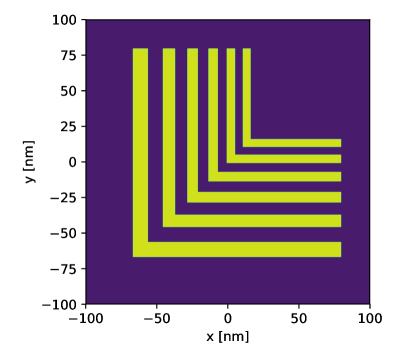
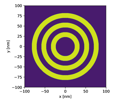

To illustrate the versatility of the theoretical method outlined in the previous sections, we now present simulation results with different source and mask parameters. To this end, we use the two target test patterns presented in Fig. 2. The first pattern [Fig. 2(a)] consists of a series of corner lines (or “L shapes”) with width and spacing decreasing from to . This is a standard pattern used for resolution testing in lithography Chang et al. (2001). Most of the simulation results that we present are obtained under the assumption of this L-shaped pattern. It should, however, be noted that the L-shaped test pattern could, in principle, also be reproduced with a free standing mask by direct imaging. That is to say, for this particular pattern, holography is not strictly necessary. To illustrate the versatility of the near-field binary-holography method, we therefore, at the end of this section, include simulation results for a second test pattern, which consists of concentric circles [Fig. 2(b)]. This pattern cannot be reproduced by direct imaging of a free-standing mask: the circular segments would fall out.
For all the simulations that we perform, the patterns are resolved into pixels and placed at a fixed distance from the mask. For the beam we use an average wavelength of , which is typical for a helium beam as discussed in the Sec. I. We use two different source configurations: (i) a plane wave (i.e., an ideal, monochromatic, perfectly coherent source) and (ii) a realistic source configuration as described in Sec. II.3, with source-mask distance of and skimmer diameter of . A wavelength distribution of has no appreciable impact on the results and is left out in the simulations presented here.
Masks can be made in two different ways: Holes can be “drilled” through a solid membrane as originally done by Fujita et al. Fujita et al. (1996). Alternatively, one can use a natural membrane and fill all of the undesired holes. This has the additional advantage of high precision because the position of the holes is built into the material. We chose our mask test parameters to reflect these two approaches. We chose one rectangular mask and one hexagonal mask, both with a hole-to-hole distance or periodicity of . This distance is chosen because it represents a natural limit of what one can imagine as possible for the density of holes in natural porous materials. The distance of is roughly the periodicity of beryl. Beryl is a silicate with a channel structure that allows individual atoms, typically metal and alkali ions, and water to be trapped in the channels. These trapped atoms were recently imaged for the first time using atomic resolution transmission electron microscopy Arivazhagan et al. (2017). One may imagine that a mask could be made by deliberate filling of selected channels with atoms, with use of, for example, a focused ion beam. Quartz has similar channels, with a thinner wall structure, which would allow an even smaller periodicity. However, the thin wall means that quartz tends to become amorphous when prepared for thin-membrane experiments. While the channels in beryl and quartz are so small that they trap larger atoms and water molecules, they are still large enough to allow smaller atoms, for example helium, to penetrate Swets et al. (1961). Holes on the order of have recently been fabricated with use of helium-ion-beam lithography, which justifies the rectangular mask Emmrich et al. (2016). Most self-organized porous membranes, including beryl, have a hexagonal structure, hence the hexagonal masks.
The masks are designed by the grid-based subdivision method, with a minimal open-hole configuration Nesse et al. (2017a) to save computation time. The same masks are used for plane-wave and realistic sources.
The rectangular mask is designed to have an array of cells, with subcells, corresponding to a maximum hole openings. The hexagonal mask is made on a grid with subcells. The mask is made from a hexagonally sampled mask field with subdivisions in a cell by the method described in the Appendix.
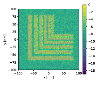
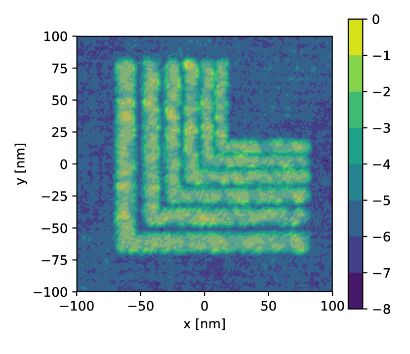
Figure 3 show the simulation results for the plane-wave source. The desired target pattern is superimposed on the actual target pattern, to illustrate how well the pattern generation works. We see that the target pattern is reproduced true to size to a precision of around . The contrast is .
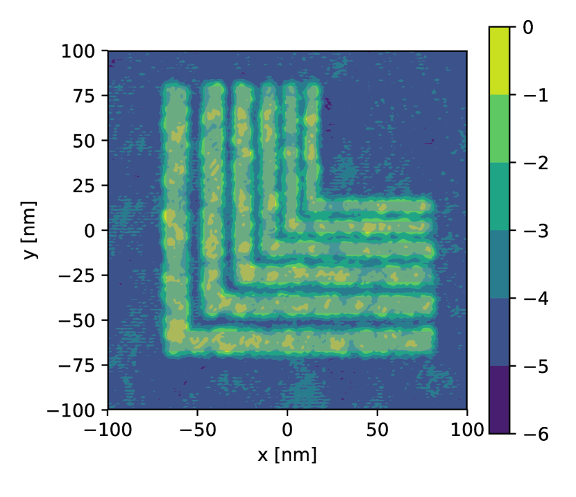
In Fig. 4 we present simulation results for the realistic source with the desired target pattern superimposed as before. The target pattern is reproduced with a precision of around and the contrast is .
Figure 5 shows the results obtained with the L-shaped pattern [Fig. 2(a)] with a realistic source and a hexagonal mask. As expected, the pattern is reproduced just as well as with the rectangular mask. The only difference is a slightly lower contrast of , which we attribute to the hexagonal mask having a smaller number of subcells in total.
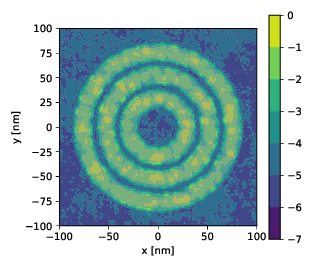
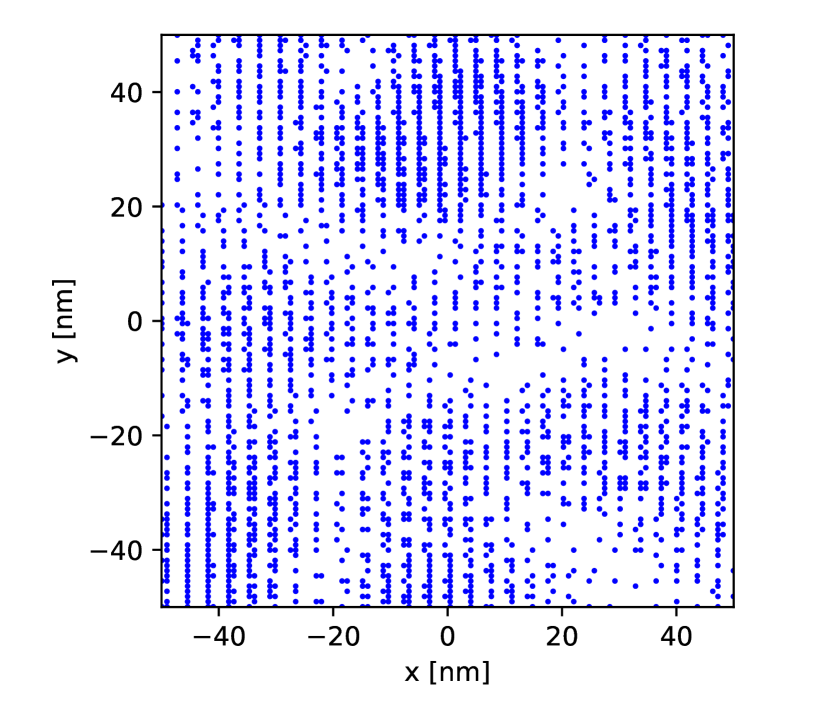
Finally, in Fig. 6 we present portion of the mask and the simulated intensity in the target plane obtained with a mask designed for the purpose of creating the concentric circular pattern in Fig. 2(a). In obtaining this result, we use the realistic source model and we discretize the target pattern onto a rectangular array of points (as was done for the L-shaped pattern). The contrast of the intensity pattern is .
Even though we have applied the near-field binary-holography technique to the successful design of the two specific patterns in Fig. 2, it should be stressed that the technique is, in principle, capable of creating arbitrary patterns. We believe that the results presented in Figs. 3–6 testify to the potential of the approach that we propose.
IV Throughput Estimation
A high wafer throughput is a necessary requirement for chip mass production. It is therefore important to consider what writing speed we can hope to achieve with a mask-based atom-lithography device and compare it with what is possible with EUV lithography. We chose here for comparison the NXE:3100 EUV tool from ASML. We use the numbers publicly available from ASML’s websites ASML (2014).
It is not trivial to make a suitable comparison. We decide simply to compare the photon flux (number of photons per second) and the atom flux (number of atoms per second). It is important to emphasize that this does not take into consideration resist performance, which is a very crucial factor. At the moment very little work has been done on resist development for metastable atoms.
We first calculate the flux for the EUV source. The power is . The energy of one EUV photon is . Thus we get a flux of .
The atom flux can be calculated on the basis of the numbers in Ref. Even (2015). For a beam with optimum, narrow velocity distribution, the experimentally measured flux from the source is atoms for a pulse. The metastable discharge works with an efficiency of giving atoms per pulse or atoms/s during the pulse.
In this perspective the atom source is comparable in efficiency to the EUV source ( atoms/s versus photons/s. However, in practice the EUV source is superior, since the valve in the pulsed source can currently operate at only while the EUV source is continuous. Also, newer EUV instruments with up to 25 times more power than given here are currently under development (NXE:3400B). Still, these simple calculations illustrate the promising potential of the metastable-atom sources for lithography.
V Conclusions and Outlook
In this paper we show how nanometer-resolution mask-based lithography of arbitrary patterns can be performed with realistic masks and atom sources. In addition we extend the binary-holography method to hexagonal cells and subcells, which makes it easier to calculate masks using self-organized porous membranes as mask substrates.
Acknowledgements.
The authors gratefully acknowledge support from the Research Council of Norway, Fripro Project 213453 and Forny Project 234159. The research of I.S. was supported in part by the Research Council of Norway Contract No. 216699 and the French National Research Agency (ANR) under contract ANR-15-CHIN-0003.Appendix A Binary holograms on hexagonal grids
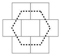
Murphy and Gallagher Murphy and Gallagher (1982) extended the binary-holography technique of Lohmann and Paris by placing the cells on a hexagonally sampled grid. The cells themselves are constructed as before, but their center points are placed on a hexagonal grid. This means that the cells are rectangular and that every other row of cells is shifted, something that must be taken into account when one is finding the correct location of each opening. The setup is illustrated in Fig. 7. The proposed use of hexagonally sampled fields would theoretically make more-accurate holograms because of the higher degree of symmetry available when circularly symmetric functions are represented. Computationally there are also potential advantages, first from a reduction in the amount of data stored and second from a reduction in the amount of work required to propagate the field between hexagonally sampled regions. Fourier methods of field propagation can be extended to work as efficiently on hexagonal grids as on rectangular grids with use of hexagonal fast Fourier transforms Mersereau (1979).
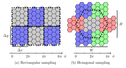
Most self-assembled porous membranes have a hexagonal structure, and we are therefore concerned with adapting binary holography to work with a hexagonal lattice of holes. We discuss the adaptation of the grid-based holography method to work with subcells placed on a hexagonal grid. This can be done in a number of ways, but here we focus on two methods. The first method works by filling out a rectangular grid of cells using hexagonal subcells [Fig. 8(a)], while the other method fills out a hexagonal grid of cells using hexagonal subcells [Fig. 8(b)].
We first discuss performing grid-based holography with hexagonal subcells by starting from a rectangularly sampled grid. Let us consider a hexagonal grid with one edge of the hexagon parallel with the axis. The full width, , of such a hexagon is related to its height, , by
| (9) |
Every other column of the grid will be shifted along the axis a half height . On such a grid we can create cells with subcells to subdivide a rectangularly sampled grid with
| (10) | ||||
| (11) |
In such a cell not all of the subcells will be aligned on the same rectangular grid, and if we assume a phase change along the axis when constructing the hologram this must be taken into account. If we have a phase change only along the axis, the contribution from each column will be the same. When such an approximation is performed, some of the subcells will overlap with the neighboring sample point. This is a natural extension of the ordinary method of grid-based holography, but it sets some limitations on the possible rectangular grids that can be used for sampling. An example of such a discretization scheme can be seen in Fig. 8(a), with .
It is also possible to adapt the method of grid-based holography to hexagonally sampled mask fields, as illustrated in Fig. 8(b). In the illustrated case we have also created rectangular cells of subcells, but now the numbers and cannot be selected freely. The cells must have the correct proportions if they are to tile hexagonally, and be of the same shape and orientation. This is possible only for even numbers of . If is odd, adjacent cells have to be flipped upside down, something that slightly moves their center. In Fig. 8(b) we have , which is one of the valid configurations. In this configuration, the repeating height is , and the repeating width is , and we see that both the width and the height are equally scaled.
Similarly to previous schemes, the next step is to assume a phase difference along the axis of across every cell and then select in which columns to open subcells and how many subcells to open. The axis of phase change is shown below the graphics in Fig. 8.
References
- ITR (2015) ITRS 2.0: International Technology Roadmap for Semiconductors, More Moore, Tech. Rep. (2015).
- Pauly (2000) H. Pauly, Atom, Molecule, and Cluster Beams I (Springer, 2000).
- Berggren et al. (1995) K. K. Berggren, A. Bard, J. L. Wilbur, J. D. Gillaspy, A. G. Helg, J. J. McClelland, S. L. Rolston, W. D. Phillips, M. Prentiss, and G. M. Whitesides, Science 269, 1255 (1995).
- Baldwin (2005) K. Baldwin, Contemp. Phys. 46, 105 (2005).
- Ueberholz et al. (2002) B. Ueberholz, S. Kuhr, D. Frese, V. Gomer, and D. Meschede, J. Phys. B 35, 4899 (2002).
- Colli (1954) L. Colli, Phys. Rev. 95, 892 (1954).
- Gardner et al. (2017) J. R. Gardner, E. M. Anciaux, and M. G. Raizen, J. Chem. Phys. 146, 081102 (2017).
- Adams et al. (1994) C. Adams, M. Sigel, and J. Mlynek, Phys. Rep. 240, 143 (1994).
- Hinderthür et al. (1998) H. Hinderthür, A. Pautz, F. Ruschewitz, K. Sengstock, and W. Ertmer, Phys. Rev. A 57, 4730 (1998).
- Eder et al. (2017) S. D. Eder, A. K. Ravn, B. Samelin, G. Bracco, A. S. Palau, T. Reisinger, E. B. Knudsen, K. Lefmann, and B. Holst, Phys. Rev. A 95, 023618 (2017).
- Koch et al. (2008) M. Koch, S. Rehbein, G. Schmahl, T. Reisinger, G. Bracco, W. E. Ernst, and B. Holst, J. Microsc. 229, 1 (2008).
- Doak et al. (1999) R. B. Doak, R. E. Grisenti, S. Rehbein, G. Schmahl, J. P. Toennies, and C. Wöll, Phys. Rev. Lett. 83, 4229 (1999).
- Carnal et al. (1991) O. Carnal, M. Sigel, T. Sleator, H. Takuma, and J. Mlynek, Phys. Rev. Lett. 67, 3231 (1991).
- Eder et al. (2015) S. D. Eder, X. Guo, T. Kaltenbacher, M. M. Greve, M. Kalläne, L. Kipp, and B. Holst, Phys. Rev. A 91, 043608 (2015).
- Eder et al. (2012) S. D. Eder, T. Reisinger, M. M. Greve, G. Bracco, and B. Holst, New J. Phys. 14, 073014 (2012).
- Patton et al. (2006) F. S. Patton, D. P. Deponte, G. S. Elliott, and S. D. Kevan, Phys. Rev. Lett. 97, 013202 (2006).
- Barr et al. (2016) M. Barr, A. Fahy, J. Martens, A. P. Jardine, D. J. Ward, J. Ellis, W. Allison, and P. C. Dastoor, Nat. Commun. 7, 10189 (2016).
- Reisinger and Holst (2008) T. Reisinger and B. Holst, J. Vac. Sci. Technol. B 26, 2374 (2008).
- Fujita et al. (1996) J. Fujita, M. Morinaga, T. Kishimoto, M. Yasuda, S. Matsui, and F. Shimizu, Nature 380, 691 (1996).
- Lohmann and Paris (1967) A. W. Lohmann and D. P. Paris, Appl. Opt. 6, 1739 (1967).
- Onoe and Kaneko (1979) M. Onoe and M. Kaneko, Electron. Commun. Jpn. 62, 118 (1979).
- Murphy and Gallagher (1982) P. K. Murphy and N. C. Gallagher, J. Opt. Soc. Am. 72, 929 (1982).
- Grisenti et al. (1999) R. E. Grisenti, W. Schöllkopf, J. P. Toennies, G. C. Hegerfeldt, and T. Köhler, Phys. Rev. Lett. 83, 1755 (1999).
- Nesse et al. (2017a) T. Nesse, J.-P. Banon, B. Holst, and I. Simonsen, Phys. Rev. Applied 8, 024011 (2017a).
- Keller et al. (2014) M. Keller, M. Kotyrba, F. Leupold, M. Singh, M. Ebner, and A. Zeilinger, Phys. Rev. A 90, 063607 (2014).
- Fouda et al. (2016) M. F. Fouda, R. Fang, J. B. Ketterson, and M. S. Shahriar, Phys. Rev. A 94, 063644 (2016).
- Bolpasi et al. (2014) V. Bolpasi, N. K. Efremidis, M. J. Morrissey, P. C. Condylis, D. Sahagun, M. Baker, and W. von Klitzing, New J. Phys. 16, 033036 (2014).
- Bennetts et al. (2017) S. Bennetts, C.-C. Chen, B. Pasquiou, and F. Schreck, Phys. Rev. Lett. 119, 223202 (2017).
- Even (2015) U. Even, EPJ Tech. Instrum. 2, 17 (2015).
- Chang et al. (2001) T. Chang, M. Mankos, K. Y. Lee, and L. P. Muray, Microelectron. Eng. 57–58, 117 (2001).
- Goodman (2005) J. W. Goodman, Introduction to Fourier Optics, McGraw-Hill physical and quantum electronics series (W. H. Freeman, 2005).
- Muffoletto et al. (2007) R. P. Muffoletto, J. M. Tyler, and J. E. Tohline, Opt. Express 15, 5631 (2007).
- Bailey and Swarztrauber (1991) D. H. Bailey and P. N. Swarztrauber, SIAM Rev. 33, 389 (1991).
- Beijerinck and Verster (1981) H. C. W. Beijerinck and N. F. Verster, Physica B+C 111, 327 (1981).
- Nesse et al. (2017b) T. Nesse, S. D. Eder, T. Kaltenbacher, J. O. Grepstad, I. Simonsen, and B. Holst, Phys. Rev. A 95, 063618 (2017b).
- DePonte et al. (2006) D. P. DePonte, S. D. Kevan, and F. S. Patton, Rev. Sci. Instrum. 77, 055107 (2006).
- Arivazhagan et al. (2017) V. Arivazhagan, F. Schmitz, P. Vullum, A. Van Helvoort, and B. Holst, J. Microsc. 265, 245 (2017).
- Swets et al. (1961) D. E. Swets, R. W. Lee, and R. C. Frank, J. Chem. Phys. 34, 17 (1961).
- Emmrich et al. (2016) D. Emmrich, A. Beyer, A. Nadzeyka, S. Bauerdick, J. C. Meyer, J. Kotakoski, and A. Gölzhäuser, Appl. Phys. Lett. 108, 163103 (2016).
- ASML (2014) ASML, “EUV lithography — NXE platform performance overview,” https://staticwww.asml.com/doclib/misc/asml_20140306_EUV_lithography_-_NXE_platform_performance_overview.pdf (2014).
- Mersereau (1979) R. M. Mersereau, Proc. IEEE 67, 930 (1979).