Coulomb blockade regions in sputter-deposited titanium nitride films
Abstract
We present topographic and spectroscopic scanning tunneling microscopy measurements taken on a 21 nm thick TiN film at a temperature of K – above the superconducting transition temperature ( K) of the sample. The film was polycrystalline with crystallite diameters of nm, consistent with other films prepared under similar conditions. The spectroscopic maps show on average a shallow V-shape around V consistent with a sample near the Mott insulation transition. In selected regions on several samples we additionally observed signs of Coulomb blockade. The corresponding peak structures are typically asymmetric with respect to bias voltage indicating coupling to two very different tunneling barriers. Furthermore, the peak structures appear with constant peak-peak spacing which indicates quantum dot states within the Coulomb blockade island. In this paper we discuss one such Coulomb blockade area and its implications in detail.
I Introduction
Titanium nitride, as a superconducting film in devices, has the useful properties of high kinetic inductance and low microwave loss. The latter property is related to the TiN film quality as well as its good material-interface formationVissers et al. (2010) which aids low noise in astronomy detectorsLeduc et al. (2010); Diener et al. (2012) and high-coherence in quantum bitsChang et al. (2013). However, the former property is perhaps the most interesting as it brings new qualitative features to recent devices. Higher kinetic inductance generally appears with a lower of the film and affects the minimum photon detection frequency in the so-called kinetic-inductance detectors. The high inductance can also enable intentional phase slips in a nanowire-based superconducting quantum bitAstafiev et al. (2012). High kinetic inductance nitrides have also been recently exploited in traveling-wave amplifiersHo Eom et al. (2012) and for tunable coupling in resonatorsBockstiegel et al. (2016).
Knowledge about the topographic and electronic structure is important for device property analysis. While there are many different growth techniques for TiNVissers et al. (2010); Jaim et al. (2015); Ohya et al. (2014); Leduc et al. (2010); Torgovkin et al. (2015) the films generally contain different crystalline orientations. The dominant orientation is correlated with resonator qualityVissers et al. (2010); Jaim et al. (2015); Ohya et al. (2014) in contrast to BCS theory of a uniform film. Anomalous qualitative features in films including excess quasiparticlesDriessen et al. (2012) and quasiparticle relaxationBueno et al. (2014) are attributed to a short mean free path or to inhomogeneity of the nitride superconductor. In a small energy range an anomalous pseudo-gap feature has been observed above related to unexpected pre-formed pairingSacépé et al. (2010). The properties above can be quite important since the kinetic inductance of TiN can be increased by proximity to a Mott-insulator non-Fermi-liquid state which suppresses the density of states at the Fermi energyAllmaier et al. (2009).
Here we discuss recent results obtained on sputter-prepared polycrystalline TiN using scanning tunneling microscopy (STM) and scanning tunneling spectroscopy (STS). The measurements were performed at a temperature of K. The superconducting transition temperature of the sample was K. Hence, the samples were observed in the normal state. The main focus was to study the topographic and electronic structure as well as their homogeneity since either conceivably influence device performance and variability.
In some regions the spectroscopic data show signs of “naturally occurring” Coulomb blockade (CB) as discussed below. Coulomb blockade in STM is usually observed when a part of the sample is coupled to the bulk of the sample by a high resistance channel similar in magnitude to the STM tunnel junction. With the STM tip acting as a second electrode, this part then behaves like the island of a fabricated single electron transistor (SET). The tip acts as the drain electrode as well as a moveable gate with a position dependent tip-island capacitance. The bulk of the sample acts as the source with a fixed capacitance and resistance value. Hence one of the telltale signs of CB in spectroscopic STM data is a systematic change of the energetic position of the CB peaks with the tip position limited to the area of the crystallite in question. Incidentally, a particle can be picked up by the tip which can lead to CB being observed throughout the image area. However, here we focus on the case of local regions of CB where the source is clearly on the sample surface. In careful examination of 47 STS maps taken over four different samples we found local CB in nanometer sized areas in 12 maps representing all samples. Considering the total area scanned in the STS maps of nm2, the presence of CB is a relatively common occurrence on our TiN samples.
II Sample preparation and measurement
The titanium nitride samples were prepared in an external DC magnetron sputtering system on a high resistivity ( , float-zone, 3 inch diameter) silicon (100) substrate. The silicon wafer was cleaned with a 49% HF solution for 30 seconds to remove the native oxide. The substrate was then placed in an O2 plasma for 30 seconds before being put into the sputtering system. During the TiN deposition, a constant pressure of 3.5 mTorr was maintained in the presence of Ar and N2, flowed at SCCM and SCCM, respectively. A power of 400 W was applied to a 3 inch Ti target for the film depositions. Pre-sputtering was performed for 1 minute without RF-bias, and an additional 30 seconds with the RF power applied to the substrate prior to opening the substrate shutterJaim et al. (2015). The substrate temperature was kept at 500 ∘C.
The wafer was cut into cm2 samples, which were mounted on an STM sample holder and sonicated in isopropanol to remove accumulated small particles due to exposure to air. After introducing them into the STM systemDreyer et al. (2010) the samples were further cleaned by heating to ∘C for minutes. During the first minutes of the heating cycle the samples were also Ar+-etched at eV ion energy and an ion flux of s-1cm-2. This preparation was found sufficient to remove insulating surface contamination without drastically changing the surface structure. The samples were then put into the STM and measured at 4.2 K. We measured the topography and took spectroscopic maps by simultaneously acquiring and curves at each point within the scan area. The curves were measured by adding a modulation to the bias voltage and detecting the signal in the tunneling current using a lock-in amplifier. The modulation frequency was Hz and the amplitude was chosen to match the respective voltage resolution of the curve to maximize the signal to noise ratio while avoiding averaging over adjacent voltage steps.
We used etched tungsten wires as STM tips. The tips were cleaned by field emission on a gold (111) single crystal. The success was verified on the gold crystal by measuring a straight, metallic curve and a work function of at least 4 eV in current vs. distance curves.
III Results and discussion
III.1 Surface structure
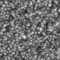
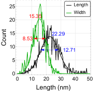
A typical topographic image of an area of nm2 is shown in Fig. 1. The films are polycrystalline with a typical diameter of nm. The grain size distribution was determined by semi-automatically segmenting the image into individual grains using MathematicaMat (2014). The algorithm used produces better results in separating crystallites than a simple watershed algorithmMeyer (2012). The individual segments are then fit to an ellipse of equal area. A histogram for the long and and short axis, respectively, are shown in Fig. 1. The means are nm and nm. The direction of the elongation however lies mostly in the x-direction and is thus at least in part due to piezo hysteresis. In atomically resolved low-temperature images at scan frequencies of 1 Hz the distortion amounts to approximately 20 % but, of course, varies with scan size and scan speed.
III.2 Spectroscopic data
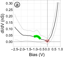
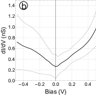
Most of the STS maps were taken in a voltage range of V. While individual spectra may vary strongly from point to point, the average shows a distinct V-shape with a clear dip at V. On a larger voltage scale the averaged spectra show a steep rise at positive bias and a peak at V. STS examples measured in two different voltage ranges and sample areas are shown in Fig. 2. The overall asymmetric structure qualitatively agrees with the calculated density of states which identifies a V-shape gap in an energy range of eV as the onset of Mott insulationAllmaier et al. (2009). We found additional local peak structures at or near zero bias as well as regions of Coulomb blockade in several areas on all samples investigated. The peaks might be gap states in the Mott insulator and will be discussed elsewhereDreyer et al. (2018). The CB states indicate that some of the crystallites or parts thereof are electronically only weakly coupled to the rest of the film network. Here we focus on one of the more striking examples of CB which also shows internal quantum dot states. While we found regions showing CB on all samples studied at 4.2 K internal quantum dot states were a rare occurrence. In the context of superconductive devices CB islands could act as sources or traps for quasiparticlesLutchyn et al. (2005, 2007) and therefore influence the coherence and performance.
III.3 Coulomb blockade

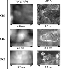


Fig. 3 shows the topography ( nm2, pA, mV) and three parts of a simultaneously obtained conductance map (“ROI”: mV, “CB1”: mV, “CB2”: mV) which show signs of CB. The areas are marked by blue boxes in the topographic image. The maps show sharp bright lines whose position shift with bias voltage indicating CB. For the remainder of this paper we focus on the largest region (marked “ROI”). The size of this region is nm2 and contains individual spectra.
To eliminate the possibility that the observed CB in “ROI” stems from a particle on the tip we compare the spectroscopy of similar regions on two different crystallites. Fig. 4 shows arrays of individual spectra from the region “R1” and “R2” marked in Fig. 3. A blue line in each of the graphs marks the averaged spectrum of the whole scan area (Fig. 2 (b)). The spectra from “R1” are virtually identical to the average. In contrast, spectra from “R2” — as well as most spectra in “ROI” — show a distinct peak structure. The peaks appear in groups with fixed peak-peak spacing within the group. The energetic position of the group as well as the peak heights vary systematically with the tip position. As the tip moves from left to right the group of peaks enters at negative and keep moving towards 0 V while diminishing in height. At frame 15 from the left the peaks are no longer visible and reappear at positive as the tip continues to move to the right.
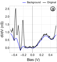
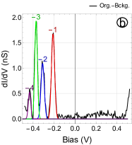
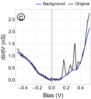
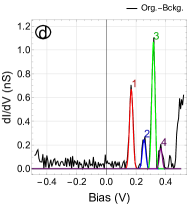
For further analysis each of the curves in “ROI” was semi-automatically searched for discernible peaks. An example of the process for two spectra marked in Fig. 4 is shown in Fig. 5. Plot (a) and (c) show the original data with an estimated background. The background is then subtracted from the data leaving sharp peaks largely unchanged as shown in plot (b) and (d). The peaks are then fit by a Gaussian function to determine position , amplitude and width . The peaks are numbered with negative/positive numbers starting with the peak closest to V. The algorithm found a total of 3359 peaks in 1165 () of the spectra of which 908 () show at least 2 peaks. A small fraction of the automatically detected peaks are erroneous.
 |
 |
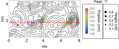 |
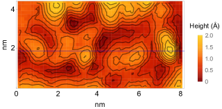
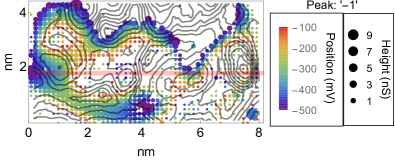
As mentioned before, one of the signatures of CB in STM measurements is a systematic change of peak position with capacitive coupling to the tip and thereby the tip position. Such a dependance is demonstrated in Fig. 6. It shows the evolution of peak “-1” and “1” in two dimensions. The peak position and height is represented by color and size of dots plotted on top of a contour plot of the topography. Since the peaks are not found in all spectra within this area a portion of the positions are left blank. In at least two core regions peak “-1” shifts towards lower energies as the tip approaches the respective center. Peak “-1” then vanishes and peak “1” appears. The latter shifts towards higher energies as the tip moves closer to the center. No correlation with topography is apparent. The details of the shift in peak position depend strongly on changes in the tip-sample capacitance and therefore on both topography and tip shape.
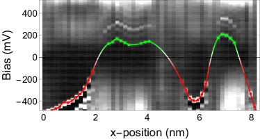
Fig. 7 shows the evolution of the spectra as the tip moves along the horizontal axis (shaded line in Fig. 6) intersecting two center regions at which peak “1” appears. The automatically found peak positions “-1” and “1” are marked by red and green dots, respectively. The dots are connected by a spline interpolation as a guide to the eye. It is clear that the peak groups exclusively appear at positive or negative bias voltages. This is an unusual behavior for CB but similar to published work on dioctyldithiophosphate sodium salt moleculesKlusek et al. (1999). There it was a hallmark of two vastly different junction resistances and capacitances in which case the junction with the higher resistance (lower tunneling rate) dominates. Here we assume an analogue situation as shown by simulations presented in the next section.
| Peaks | Count | Position (mV) | (mV) |
| 425 | 102 | 4.0 | |
| 327 | 63 | 3.4 | |
| 166 | 62 | 4.4 | |
| 33 | 87 | 3.1 | |
| “” | 50 | 142 | 6.8 |
| 66 | 62 | 3.6 |
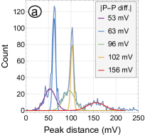
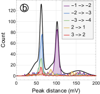
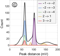
Finally, we analyze the distance between neighboring peaks within the spectra. Fig. 8 (a) shows a histogram of all distances found in “ROI”. The resulting distribution is well approximated by five Gaussian functions. However, an analysis considering the origin of the distance — i.e. the peak numbers involved — gives a more refined picture. Fig. 8 (b) shows histograms of the five most common pairs. For comparison the outline of the overall histogram is also shown. Again, the histogram peaks (HP) were fit by Gaussians and the result is shown in Fig. 8 (c) and summarized in Table 1. The HP positions fall into two groups: the innermost ones ( meV and meV) and the rest around meV. The additional HP of meV stems mostly from missing the relatively small peak “2” in our automatic peak detection and thus measuring the distance instead. The quantum dot states show an identical level spacing when appearing on the positive/negative bias side of meV except for the first distances. While the QD is geometrically defined the ground state might depend on the bias polarity or QD charging state. As we will show in the next section the switch of the peaks from negative to positive sample bias is indeed accompanied by the addition of one electron to the QD. This could explain the difference between and .
III.4 Simulations

| Parameter | STM junction (1) | Sample junction (2) |
|---|---|---|
| Resistance | 1.67 G | 20 M |
| Capacitance | 0.1–0.2 aF | 1 zF |
| Temperature | 4.2 K | |
Previous observations of Coulomb blockade using STM were performed mostly on special samples of small metallic particles at room temperatureKano et al. (2015); Pryadko et al. (2000); Amman et al. (1993) or low temperatureHong et al. (2013); Pal et al. (2011); Miller et al. (1994); Sch nenberger et al. (1993); Klusek et al. (1999); Liljeroth et al. (2006); Qiao et al. (2017). All of these observations are usually explained by orthodox Coulomb blockade theoryAmman et al. (1991); Hanna and Tinkham (1991) which calculates the tunnel rates between two electrodes and an island and thus the resulting current flow between the electrodes. These calculations allow the estimation of the resistance and capacitance of the two junctions as well as the fractional electron charge on the island. The absence of a dedicated gate electrode limits the analysis compared to a regular SET circuit.
In our data it is clear that while the peak groups shift with tip position the distances within the group remain constant. This is consistent with tunneling through a quantum dot with internal states. A detailed simulation such as given for a semiconducting QD inLiljeroth et al. (2006) is beyond the scope of this paper. However, some of the behavior can be explained using orthodox CB theory. We only consider the position and height of the innermost peaks (“-1” and “1”). The energy of peak can be expressed analytically by the junction capacitance and and the fractional charge on the island by
and
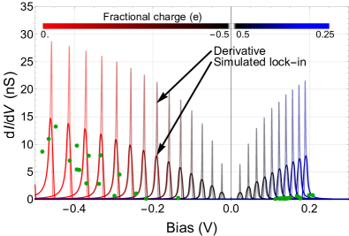
Here, however, we only observe a single CB peak in each spectrum which leaves no practical way to decouple the parameters , , and . Therefore we use the correlation between peak height and position as a function of as the principle driver. Fig. 9 shows the proposed behavior. We assume that the tip carries a positive charge conceivably in remaining oxide layers near the apex. As the tip moves across the CB island it induces an increasing negative fractional charge on the island from towards . This change in moves the position of the lead peak of the CB from negative bias voltages towards zero. At the same time the peak height diminishes. Reducing beyond leads to a charging event of the island by adding one electron. This change in charge might also be responsible for the difference in the peak and distance we observed. As the tip proceeds to move towards the (electronic) center of the island decreases from now towards zero. This shifts the lead CB peak towards positive voltages while its height grows again. The sequence reverses as the tip moves past the center of the island.
We applied two methods to compute the conductance () from the curves calculated using orthodox theory. Numerical differentiation leads to sharp peaks only thermally broadened by K. The second method simulates a lock-in amplifier using our modulation amplitude of mV. This results in broader and shallower peaks which decrease faster in height. Fig. 10 compares the result of the simulation with the observed peak height vs. position. The parameters for the simulation are summarized in table 2. The resistance of the STM junction was taken from the bias voltage and current set point of mV and nA ( G). A sample junction of M then sets the overall height of the conductance peaks to roughly match the observed values of up to 15 nS. The sample side capacitance as well as the STM junction capacitance value were chosen to be small enough so that only a single peak appears within the STS window of mV. was also allowed to increase as the tip approaches the center which accounts for the increase in peak density at positive bias voltages in the simulation. Finally, is varied from -.05 to -.45 to shift the peak from -0.5 V towards 0 V. This also reduces its height (red curves in Fig. 10). Further reduction in leads to a charging event changing the number of electrons by one (which is unimportant in this model), switching to 0.45 and moving the peak to the positive bias side. As continues to decrease, the peak shifts towards more positive bias voltages and it’s height increases again (blue curves in Fig. 10. Green dots mark the measured peak height vs. position. While the overall trend is well reproduced the peak heights diminish faster in our measurements than in the simulation. This discrepancy could be due to the quantum dot nature of the Coulomb blockade island or due to the background density of states of the TiN sample which was not considered in the simulation.
IV Conclusion
We performed an STM study at 4.2 K of a polycrystalline TiN film with nm diameter crystallites. STS measurements taken over a few hundred mV show a pseudo-gap at V, similar to theoretical DFT calculations near Mott insulation. In certain locations we observed Coulomb blockade peaks as well as quantum dot states. The behavior of the Coulomb blockade peaks were explained by orthodox theory. The fractional charge on the CB island changes with tip position which in turn moves the energetic position and height of the CB peaks. While the energy spacing is too large to directly interfere with typical microwave devices operating in the GHz regime ( ), both the quantum dot and Coulomb blockade can act as a source or a trap of quasiparticles. Since CB regions were found on all samples their density has to be considerable in films prepared under similar conditions (here 1 in 266 nm2). If these anomalous CB features are generic to TiN films, it would be interesting to explore the effects on device performance made by a gate which can change the charging state of the CB ensemble.
Appendix A Mathematica code
A.1 Automatic peak detection
The Mathematica code for the automatic peak detection in the spectra is shown below. ddsb contains all curves with the background removed using the Mathematica function EstimatedBackground with a scale parameter of 5. vlt contains a list of the voltages corresponding to the points on the curves.
A.2 Orthodox Coulomb blockade
Mathematica code for calculating the Coulomb blockade tunneling current.
A.3 Calculation of dI/dV
Using Mathematicas symbolic differentiation function D the derivative of the expression for the current with respect to the bias voltage is first calculated. The resulting formula is the used to generate the plot.
The lock-in simulation is based on a convolution of the curve with one period of a cosine function while modulating the bias voltage, i.e.:
References
- Vissers et al. (2010) M. R. Vissers, J. Gao, D. S. Wisbey, D. A. Hite, C. C. Tsuei, A. D. Corcoles, M. Steffen, and D. P. Pappas, Appl. Phys. Lett. 97, 232509 (2010), http://dx.doi.org/10.1063/1.3517252 .
- Leduc et al. (2010) H. G. Leduc, B. Bumble, P. K. Day, B. H. Eom, J. Gao, S. Golwala, B. A. Mazin, S. McHugh, A. Merrill, D. C. Moore, O. Noroozian, A. D. Turner, and J. Zmuidzinas, Appl. Phys. Lett. 97, 102509 (2010), http://dx.doi.org/10.1063/1.3480420 .
- Diener et al. (2012) P. Diener, H. G. Leduc, S. J. C. Yates, Y. J. Y. Lankwarden, and J. J. A. Baselmans, J. of Low Temp. Phys. 167, 305 (2012).
- Chang et al. (2013) J. B. Chang, M. R. Vissers, A. D. C rcoles, M. Sandberg, J. Gao, D. W. Abraham, J. M. Chow, J. M. Gambetta, M. B. Rothwell, G. A. Keefe, M. Steffen, and D. P. Pappas, Appl. Phys. Lett. 103, 012602 (2013), http://dx.doi.org/10.1063/1.4813269 .
- Astafiev et al. (2012) O. V. Astafiev, L. B. Ioffe, S. Kafanov, Y. A. Pashkin, K. Y. Arutyunov, D. Shahar, O. Cohen, and J. S. Tsai, Nature 484, 355 (2012).
- Ho Eom et al. (2012) B. Ho Eom, P. K. Day, H. G. LeDuc, and J. Zmuidzinas, Nat. Phys. 8, 623 (2012).
- Bockstiegel et al. (2016) C. Bockstiegel, Y. Wang, M. R. Vissers, L. F. Wei, S. Chaudhuri, J. Hubmayr, and J. Gao, Appl. Phys. Lett. 108, 222604 (2016), https://doi.org/10.1063/1.4953209 .
- Jaim et al. (2015) H. M. I. Jaim, J. A. Aguilar, B. Sarabi, Y. J. Rosen, A. N. Ramanayaka, E. H. Lock, C. J. K. Richardson, and K. D. Osborn, IEEE Trans. on Appl. Sup. 25, 1 (2015).
- Ohya et al. (2014) S. Ohya, B. Chiaro, A. Megrant, C. Neill, R. Barends, Y. Chen, J. Kelly, D. Low, J. Mutus, P. J. J. O Malley, P. Roushan, D. Sank, A. Vainsencher, J. Wenner, T. C. White, Y. Yin, B. D. Schultz, C. J. Palmstr m, B. A. Mazin, A. N. Cleland, and J. M. Martinis, Sup. Sci. and Tech. 27, 015009 (2014).
- Torgovkin et al. (2015) A. Torgovkin, S. Chaudhuri, J. Malm, T. Sajavaara, and I. J. Maasilta, IEEE Trans. on Appl. Sup. 25, 1 (2015).
- Driessen et al. (2012) E. F. C. Driessen, P. C. J. J. Coumou, R. R. Tromp, P. J. de Visser, and T. M. Klapwijk, Phys. Rev. Lett. 109, 107003 (2012).
- Bueno et al. (2014) J. Bueno, P. C. J. J. Coumou, G. Zheng, P. J. de Visser, T. M. Klapwijk, E. F. C. Driessen, S. Doyle, and J. J. A. Baselmans, Appl. Phys. Lett. 105, 192601 (2014), https://doi.org/10.1063/1.4901536 .
- Sacépé et al. (2010) B. Sacépé, C. Chapelier, T. I. Baturina, V. M. Vinokur, M. R. Baklanov, and M. Sanquer, Nat. Comm. 1, 140 (2010).
- Allmaier et al. (2009) H. Allmaier, L. Chioncel, and E. Arrigoni, Phys. Rev. B 79, 235126 (2009).
- Dreyer et al. (2010) M. Dreyer, J. Lee, H. Wang, and B. Barker, Review of Scientific Instruments 81, 053703 (2010).
- Mat (2014) Wolfram Mathematica 10, Wolfram Research, Inc. (2014).
- Meyer (2012) F. Meyer, ArXiv e-prints (2012), arXiv:1202.0216 [cs.CV] .
- Dreyer et al. (2018) M. Dreyer, P. Xu, K. D. Osborn, and R. E. Butera, (to be published) (2018).
- Lutchyn et al. (2005) R. Lutchyn, L. Glazman, and A. Larkin, Phys. Rev. B 72, 014517 (2005).
- Lutchyn et al. (2007) R. Lutchyn, L. Glazman, and A. Larkin, Phys. Rev. B 76, 069902 (2007).
- Klusek et al. (1999) Z. Klusek, M. Luczak, and W. Olejniczak, Applied Surface Science 151, 262 (1999).
- Kano et al. (2015) S. Kano, T. Tada, and Y. Majima, Chem. Soc. Rev. 44, 970 (2015).
- Pryadko et al. (2000) L. P. Pryadko, E. Shimshoni, and A. Auerbach, Phys. Rev. B 61, 10929 (2000).
- Amman et al. (1993) M. Amman, S. B. Field, and R. C. Jaklevic, Phys. Rev. B 48, 12104 (1993).
- Hong et al. (2013) I.-P. Hong, C. Brun, M. Pivetta, F. c. Patthey, and W.-D. Schneider, Front. Phys. 1, 13 (2013).
- Pal et al. (2011) S. S. Pal, K. Schouteden, and C. V. Haesendonck, Journal of Applied Physics 110, 044314 (2011), http://dx.doi.org/10.1063/1.3624952 .
- Miller et al. (1994) T. G. Miller, R. Reifenberger, M. McElfresh, D. W. Face, and W. L. Holstein, Journal of Low Temperature Physics 94, 239 (1994).
- Sch nenberger et al. (1993) C. Sch nenberger, H. van Houten, J. Kerkhof, and H. Donkersloot, Applied Surface Science 67, 222 (1993).
- Liljeroth et al. (2006) P. Liljeroth, L. Jdira, K. Overgaag, B. Grandidier, S. Speller, and D. Vanmaekelbergh, Phys. Chem. Chem. Phys. 8, 3845 (2006).
- Qiao et al. (2017) J.-B. Qiao, H. Jiang, H. Liu, H. Yang, N. Yang, K.-Y. Qiao, and L. He, Phys. Rev. B 95, 081409 (2017).
- Amman et al. (1991) M. Amman, R. Wilkins, E. Ben-Jacob, P. D. Maker, and R. C. Jaklevic, Phys. Rev. B 43, 1146 (1991).
- Hanna and Tinkham (1991) A. E. Hanna and M. Tinkham, Phys. Rev. B 44, 5919 (1991).