First principles calculations of band offsets at heterovalent -Ge/InxAl1-xAs interfaces
Abstract
First-principles electronic structure calculations are carried out to investigate the band alignments of tensile strained (001) Ge interfaced with (001) InxAl1-xAs. The sensitivities of band offsets to interfacial structure, interfacial stoichiometry, and substrate stoichiometry, are investigated. Large qualitative variations of the valence and conduction band offsets are observed, including changes of the band offset type, indicating the importance of local structural variations of the interface for band offsets in real samples. Our results explain recent measurements of band offsets derived from XPS core level spectra in terms of As atoms penetrating through the first few monolayers of the Ge film. Analogous studies are carried out for the diffusion of other species across the interface, and in general, the band offsets vary approximately linearly with diffusion depth relative to the values for pristine “sharp” interfaces, where the sign of the linear variation depends on the diffusing species. This large sensitivity of the band alignments to interface details indicates potential routes to chemically control the band offset of this group-IV/III-V interface by tuning the stoichiometry of the substrate surface that the thin-film is grown on.
I Introduction
The interface of tensile strained germanium (-Ge) grown on III-V substrates is currently being considered as the working tunnel-barrier in the channel of future high-performance and low-power consumption tunnel field-effect transistors (TFETs).Hudait et al. (2014); Clavel et al. (2015); Nguyen et al. (2015) These devices take advantage of band-to-band tunneling of charge carriers between the source and drain, and as a result, can overcome the limit for the subthreshold slope of thermionic devices,Ionescu and Riel (2014) thereby simultaneously improving the transistor switching speed (performance) and I/I current ratio (power efficiency). Concurrently, there is a large research effort dedicated to the integration of optical interconnects on a CMOS compatible platform,Miller (2009); Assefa et al. (2010) allowing for highly efficient ultrafast inter- and intra-chip data communication. The latter requires efficient on-chip light sources, and -Ge grown on III-V substratesPavarelli et al. (2013) is being investigated for this purpose due to the tensile strain induced direct band gap of Ge.
The operation of transistor devices depends crucially on the junctions at the border between device materials, and this dependence only becomes stronger as device dimensions continue to shrink.del Alamo (2011); Ferain et al. (2011) From the perspective of optical devices, where electron-hole recombination is required in the active region for light emission, material interfaces also play a dominant role in the device operationPavarelli et al. (2013) by determining the barrier height for electron and hole confinement. Motivated by the technological importance, significant progress has been made in recent decades towards the understanding of solid-state interfaces and the resulting line up of energy bands between materials forming the interface.Peressi et al. (1998); Margaritondo (2012); Agostini and Lamberti (2013); Brillson (2016)
In terms of ab-initio calculations of band alignments, the lattice-matched isovalent interfacesVan de Walle and Martin (1987); Vandenberg et al. (1988); Christensen (1988); Peressi et al. (1990); Hybertsen (1990, 1991) represent the simplest and most well studied category. Density functional theory (DFT) is typically employed, and idealized, atomically abrupt interfacial structuresHarrison et al. (1978); Peressi et al. (1998) are often used. These theoretical works have shown that band alignments for these interfaces are predominantly derived from bulk properties of the adjoining materials.Van de Walle and Martin (1987); Christensen (1988) Hence, for isovalent interfaces, the interfacial structure does not have a significant effect.
Band offsets (BOs) across pseudomorphic heterostructures exhibiting heterovalent bonding across the interface have also been studied, both experimentallyWaldrop and Grant (1979); Kraut et al. (1980); Biasiol et al. (1992); Dahmen et al. (1993); Volodin et al. (2014); Pavarelli et al. (2013) and computationally.Martin (1980); Kunc and Martin (1981); Peressi et al. (1991); Biasiol et al. (1992); Franciosi et al. (1993); Peressi et al. (1998); Pavarelli et al. (2013) As for the isovalent interfaces, a large portion of the computational (atomistic modeling) studies also involve ideal, abrupt interfaces, although some focus has been given to atomic intermixing/diffusion across the interface.Peressi et al. (1998) Unlike isovalent junctions, the interfacial structure can have a significant effect on the band offsets of heterovalent interfaces, to the point of inducing qualitative modifications to the offsets, e.g. type-I to type-II or vice versa, in interfaces such as -Ge/In0.3Ga0.7As(001),Pavarelli et al. (2013) and also for Ge/InxAl1-xAs(001) in certain cases (see results section).
In this paper, the sensitivity of BOs to interface structure in the lattice (mis)matched heterovalent (-)Ge/InxAl1-xAs(001) interface is explained by a linear response electrostatic effectResta et al. (1989); Peressi et al. (1998) which occurs as a result of changes in the position of polarized bonds (IV-III, or IV-V) relative to the abrupt interface. Local changes in the electrostatic potential step across the junction result from the local variations in valence charge density and the latter are in turn induced by variations in the stoichiometry of the interfacial region. Hence, this work extends previous theories of BO-interface structure relationsResta et al. (1989); Peressi et al. (1998) to the technologically important interface (-)Ge/InxAl1-xAs(001). By explaining the qualitative changes in the band alignments that can be achieved for the same material interface by only changing the interface structure, this work also contributes to the understanding of how devices can be tailored by the interface.
Lattice mismatching across the interface can also affect the band alignment. When a thin-film is grown pseudomorphically on a substrate with a different lattice constant the thin-film exhibits elastic strain so that it can match the lattice constant of the substrate, below a critical thickness such that stress is not large enough to cause plastic relaxation via e.g. dislocation formation.Chason and Guduru (2016) Epitaxial strain can be used to induce a direct bandgap in Ge, useful for silicon-compatible photonics.Liang and Bowers (2010) For strained, heterovalent interfaces such as (-)Ge/InxAl1-xAs the dependence of the band alignment on tensile strain , which is varied by the substrate stoichiometry , can be significant due to the reordering of conduction band valleys. Here, we study the band alignment over a range of cation stoichiometry and show that when combined with modifications of the interface structure (modifications which represent diffusion of group-III atoms into the Ge layer), transitions between type-I and type-II band alignments can be achieved in this interface.
In this work, the variations of valence (VBO) and conduction (CBO) band offsets between Ge and InxAl1-xAs, with respect to interfacial configuration, are investigated using first-principles atomistic simulations—which are detailed in the next section. In Sec. III, we consider a range of systematic structural modifications of the interface. Specifically, we consider (a) the Ge, As, and group-III stoichiometric balance of the mixed interfacial region for fixed substrate stoichiometries, (b) group-III composition of the InxAl1-xAs substrate (for = 0.0 to 0.25) for fixed interfacial stoichiometries (Sec. III.1), (c) interdiffusion of species across the junction (Sec. III.2). For interdiffusion, we investigate the relative stability of diffused atoms in either material (Sec. III.2.4). Finally, in Sec. III.3, we rationalize the results by simple arguments and models based on the linear response electrostatic effect. Based on the results of the simulations and on the linear response analysis, we conclude (Sec. IV) that our simulations provide a picture consistent with existing experimental results. We predict that both type-I and type-II band offsets should be observable for this interface depending on the details of the interface structure.
II Computational Methods
Optimized geometries of bulk and interface models are calculated using DFT within the local density approximation (LDA),Perdew and Zunger (1981); Perdew and Wang (1992) along with a plane wave basis set and norm-conserving pseudopotentialsTroullier and Martins (1991), as implemented in the Quantum Espresso software suite.Giannozzi et al. (2009) A non-linear core correction is added to the In pseudopotential to treat the core-valence interaction.Louie et al. (1982) 50 Rydberg kinetic energy cutoff is used for the plane wave basis set. Numerically converged Monkhorst-PackMonkhorst and Pack (1976) -point grids are used for all supercells in this work. The macroscopic average along the axis (aligned to the (001) direction) of the planar average (parallel to the interfacial plane) of the self-consistent potentialBaldereschi et al. (1988) [m] for bulk and interface cells are calculated within DFT.Giantomassi et al. (2011) Interface models consist of 24 atomic layers oriented along the (001) direction; 11 monolayers for Ge, 11 monolayers for InxAl1-xAs, and at least 1 mixed monolayer per periodic image of the supercell. Parallel to the interface, interface supercells have dimensions of () in units of the (110) lattice parameter. The virtual crystal approximation (VCA) is used to approximate the InxAl1-xAs cation alloy for each composition point.
Bulk cells are used to calculate the bulk band edges relative to the respective m for each material, and interface cells are used to calculate the potential offset (, see below) between the slabs. All band offsets correspond to fully relaxed geometries for bulk InxAl1-xAs and interface cells, while for Ge the bulk cells are biaxially strained along the (100) and (010) directions and allowed to relax along (001). Thus, the bulk cells represent biaxially tensile strained Ge grown on an InxAl1-xAs substrate (with AlAs lattice matched to Ge) and the interface models represent the minimum energy bonding configuration between the slabs.
In order to investigate the relative stability of diffused impurities in either Ge or AlAs, large cubic bulk cells with dimensions (333) in units of the (100) lattice parameter are used to calculate the formation energiesVan de Walle and Neugebauer (2004); Freysoldt et al. (2014) of substitutional impurities in bulk Ge and bulk AlAs. 111We do not consider InxAl1-xAs with 0 for this purpose due to the inaccurate bond lengths resulting from the VCA approach which would lead to inaccurate impurity-host bonding energies. These correspond to impurity defects present after growth as a result of diffusion of substrate species during growth of the material on the substrate. Thus, we consider a single Al (As) on a Ge site (Al(As)) in a 216 atom bulk Ge supercell, and a single Ge on an Al (As) site (Ge) in a 216 atom bulk AlAs cell. The formation energies are calculated as a function of the chemical potential α of each exchanged atom Van de Walle and Neugebauer (2004); Freysoldt et al. (2014) which are related to the bulk elemental phases to establish boundaries on α. Thus, the formation energies can be calculated for As-rich and Al-rich conditions, where the range of variation of As and Al chemical potentials corresponds to the heat of formation of AlAsZhang and Northrup (1991).
Thermodynamically stable configurations correspond to charge neutral interfacial bonding configurations between group-IV and group-III/V atomsPeressi et al. (1998); Martin (1980); Kunc and Martin (1981); Bylander and Kleinman (1990) with no electric field building up across either material. In supercell simulations, the lack of a slab dipole is ensured when NIV-V = NIV-III, where NIV-V(III) is the number of Ge-V(Ge-III) bonds per simulation cell. This constraint is imposed in all simulations in this work.
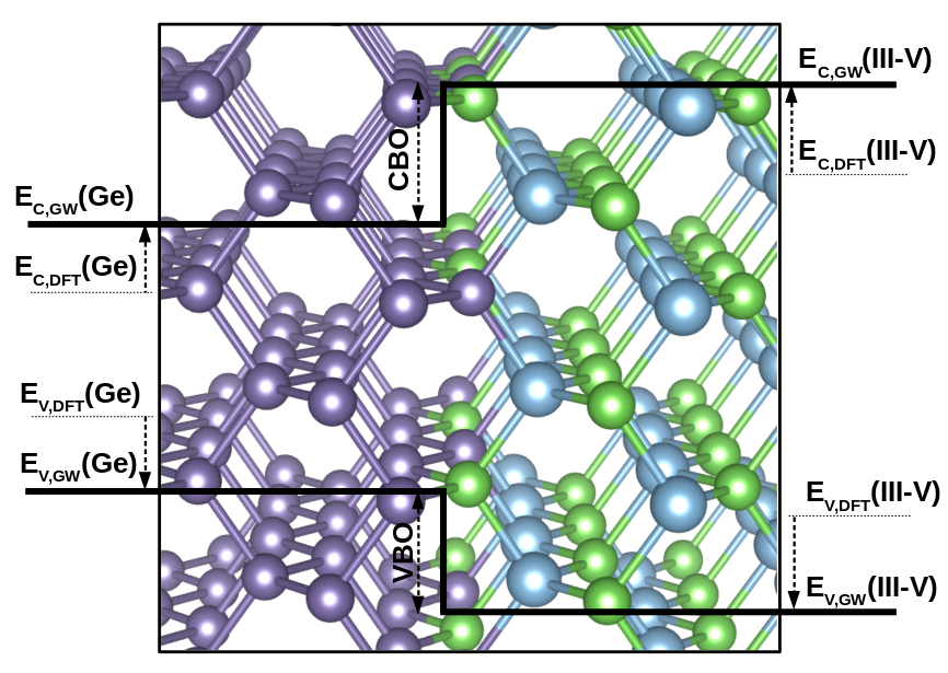
Clearly, accurate band offsets require accurate calculations of the bulk band structures, which is precluded in DFT due to the well-known band gap problem.Perdew et al. (1982); Sham and Schlüter (1985); Godby et al. (1988) The DFT+ approach corrects the energy levels using the approximation to the electron self-energyHedin (1965); Aryasetiawan and Gunnarsson (1998); Hybertsen and Louie (1986) providing sufficiently accurate bulk band structures for evaluating band alignments at semiconductor/oxide interfaces.Grüning et al. (2010); Giantomassi et al. (2011) In this work, differences of 0.17 eV between the VBO calculated with and without the correction are found for the lattice matched Ge/AlAs(001) and for lattice mismatched -Ge/InxAl1-xAs(001). For these reasons, all VBOs and CBOs calculated in this work are obtained using the DFT+ approach. This yields a first-order approximation to the quasiparticle band gaps from which band offsets are derived.Grüning et al. (2010); Giantomassi et al. (2011) Valence and conduction band offsets are computed using
| (1) |
| (2) |
where () is the valence band maximum of Ge (InxAl1-xAs) relative to of the bulk cells, () is the DFT conduction band minimum of Ge (InxAl1-xAs) relative to (), () is the GW correction to the valence band maximum (conduction band minimum) and () represents the difference between the materials in the GW correction for the valence/conduction band edge (V/CBE). is the offset in m across the interface. To obtain , the entire self-consistent potential was taken, however the change in across the interface does not significantly involve the exchange-correlation potential, which is flat throughout the interface cell. For unstrained Ge, the conduction band minimum resides at the L point, while for sufficient biaxial strain Ge Ge exhibits a direct minimum gap. After relaxing the lattice constants of AlAs and InAs, and assuming a linear variation of the InxAl1-xAs lattice constant with , the corresponding change in cell parameters is applied to the relaxed Ge cell, resulting in Ge = 1.76% when In content = 0.25. As discussed in the results section, the varying In content affects the ordering of the satellite valleys of both Ge and In, which has important implications for the band offsets.
We note that no spin-orbit coupling (SOC) is included in these calculations. The effect of SOC is to split the heavy hole states (with = 1/2 angular momentum) near the top of the valence band. This splitting is 0.30 eV in Ge, and 0.275 eV in AlAsMadelung (2004). As this difference of 0.025 eV is relatively small, we expect a correspondingly small effect on our calculated band offsets, which in this work always correspond to the offset between band extrema. Hence, we consider the gain in accuracy to be insufficient to justify the increased computational load of including relativistic terms, and we omit SOC.
III Results
III.1 Abrupt ordered interfaces
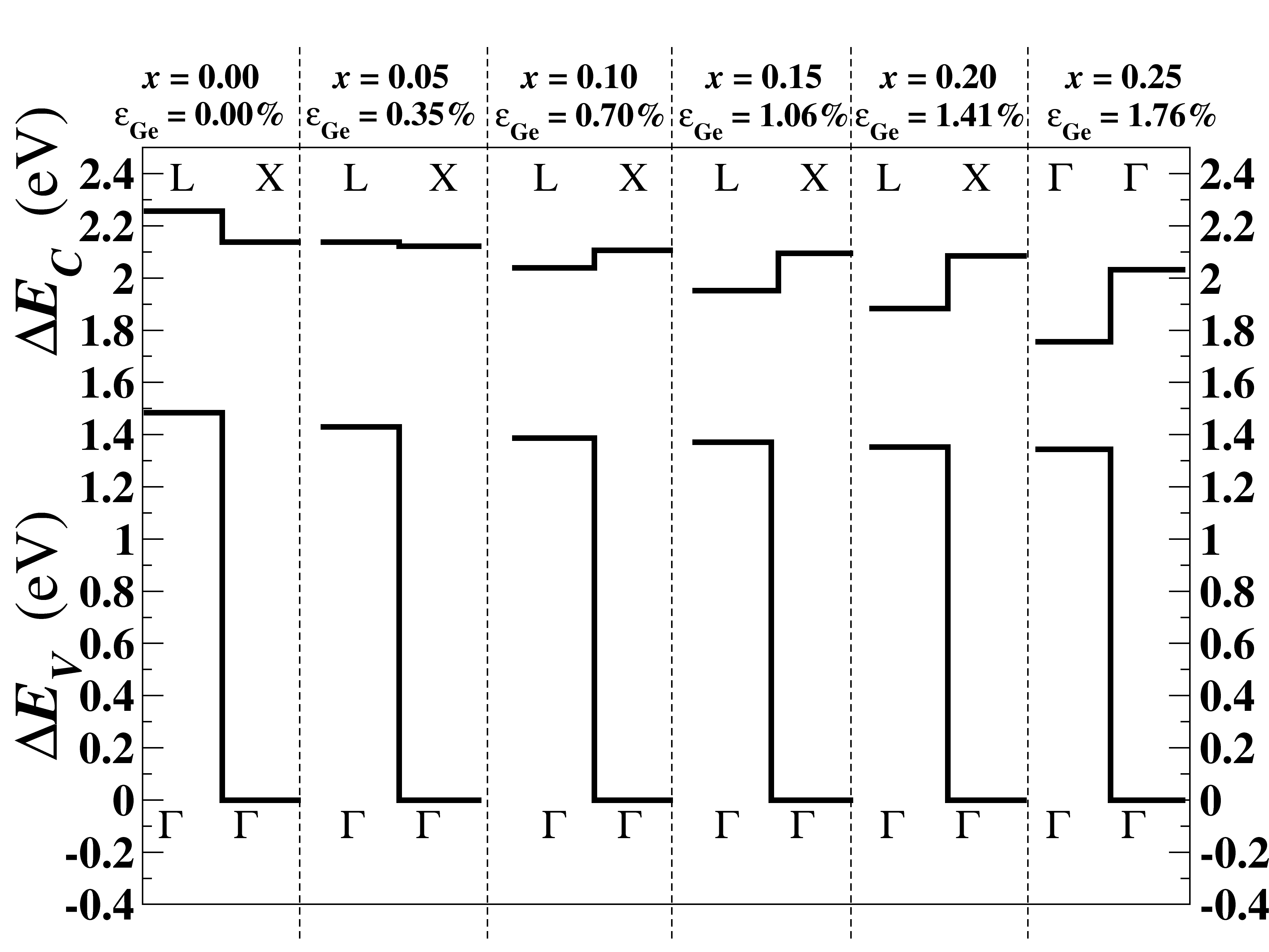
In this section, we focus on the interface that is atomically abrupt and localized to a single mixed monolayer which resides precisely between the slabs forming the heterojunction. The mixed interfacial monolayer (MIML) consists of either Ge and As atoms, or of Ge and In/Al atoms. This is exemplified by the ordered interface shown in Fig. 1. No interdiffusion is considered at this stage. Considering this as a fixed interfacial configuration, the InxAl1-x stoichiometry of the substrate is varied from = 0 to = 0.25 and the valence and conduction band offsets are tracked in steps of = 0.05. Varying the In content affects the lattice constant of the substrate which in turn changes the strain state of the Ge slab. As Ge increases beyond 1.5%, the conduction band satellite valleys are reordered in energy and Ge becomes a direct gap material. An analogous statement can be made for the conduction band valleys of InxAl1-xAs. Our calculations show that for 0.20, the minimum energy valley in InxAl1-xAs resides at the X point, while for larger proportions of In, InxAl1-xAs exhibits a direct minimum gap at .
In recent experimental works, III-V substrate growth is immediately followed by cooling under an As2 overpressure before transfer to a vacuum chamber for Ge growth,Clavel et al. (2015) such that the resulting heterostructure most likely corresponds to Ge grown on an As-terminated InxAl1-x slab, rendering an interfacial layer consisting of Ge and As atoms. In other experimental studies, group-III precursors was introduced immediately prior to Ge growth,Cheng et al. (2012) or even coverages of group-III and V atoms on the III-V surface before Ge growth were inferred from the observed surface reconstructionMaeda et al. (1995) with significant III segregation into Ge after Ge growth.Maeda and Tanaka (1999) All of these studies taken together provide an impetus to study both III-terminated and V-terminated InxAl1-xAs interfaced with Ge. As will be shown below, alternative interfacial stoichiometries can lead to interesting behavior in the form of qualitative changes to the band alignments. Hence, we study BOs for both cases, starting with the interface in which InxAl1-xAs is As terminated (see Fig. 1 for structure). The results are displayed in Fig. 2.

With the interfacial configuration fixed to that shown in Fig. 1 (group-V-terminated), a relatively small change in the valence band alignment is observed as a function of In content; 0.11 eV change in the VBO is observed between = 0.00 and = 0.25. The CBO exhibits a larger change of 0.47 eV as a function of In content. Thus a type-I BO is observed for Ge interfaced with As-terminated InxAl1-xAs, and modifications of the group-III composition of the substrate for 0.00 0.25 (neglecting changes due to the randomized cation alloy) does not qualitatively change the band alignment.
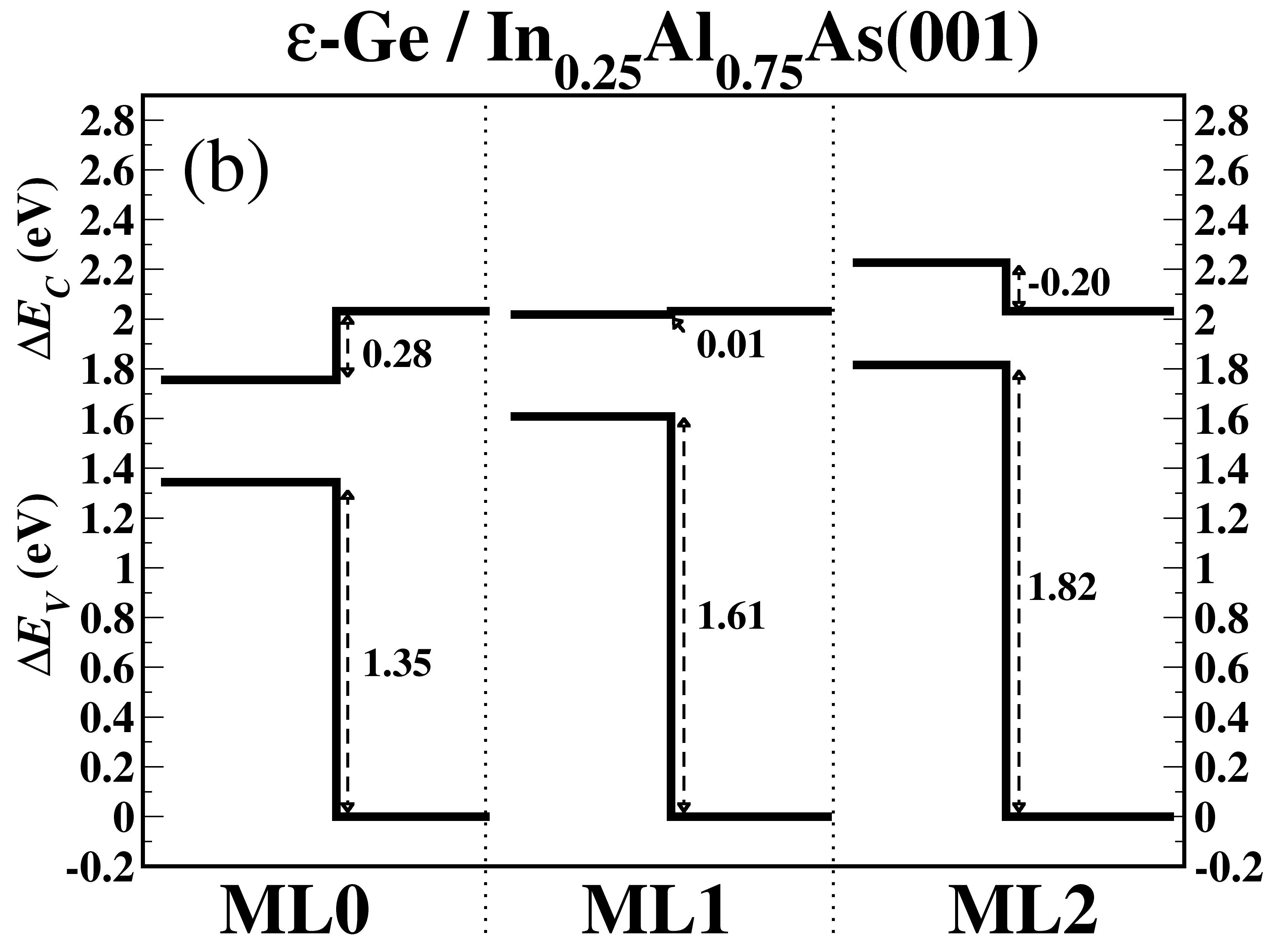
Changing to the group-III-terminated InxAl1-xAs, in which the MIML consists of Ge and In/Al cation atoms, a stark contrast is observed in the band alignments compared to the As-terminated case. Fig. 3 shows much larger VBOs and correspondingly smaller CBOs, with the CBO becoming negative (corresponding to the Ge CBE being higher in energy than that of InxAl1-xAs, see equation (2)) for small values of ; a type-II band offset is calculated for 0.05, and so a type-II to type-I transition in the band alignment occurs as a function of III content for the abrupt III-terminated -Ge/InxAl1-x(001) interface, with the BOs being type-I for 0.05.
In addition to showing the BO dependence on substrate stoichiometry, this is also a strong indication of the high sensitivity of band alignments to interfacial stoichiometry for -Ge/InxAl1-xAs(001) (compare Figs. 2 and 3 for a given value of ), and shows that the band alignment can also change from type-I to type-II when comparing As-terminated to III-terminated Ge/AlAs interfaces. This is in qualitative agreement with the results of Pavarelli et al.Pavarelli et al. (2013) who reported an analogous change in the calculated band offset type for anion and cation dominated interface stoichiometries in the -Ge/In0.3Ga0.7As(001) interface. The results also indicate a comparable change in the VBO and CBO as a function of In content for both the III-terminated case and the As-terminated case, although a slightly larger change is seen for the III-terminated case. This is explained by the presence of group-III atoms at the interface. As the latter corresponds to a III rich InxAl1-xAs surface, the larger variation of the VBO (0.15 eV) and CBO (0.5 eV) with respect to the InxAl1-x stoichiometry is observed due to the slightly larger effect that has on the interface potential term , where the latter is derived from the atomic potentials present in the interface supercell.
III.2 Interdiffusion
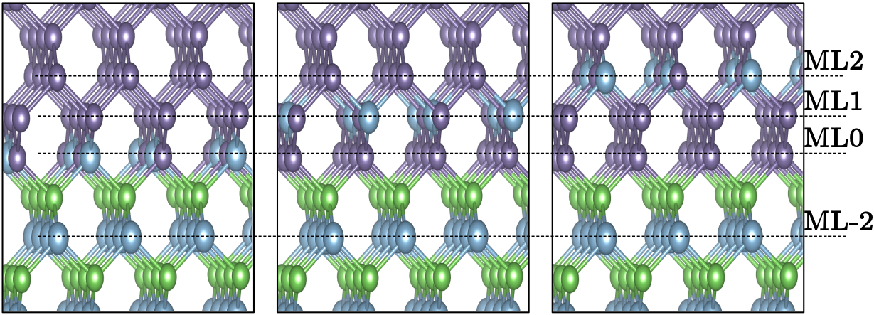
In order to investigate the effects of interdiffusion of atomic species across the interface on band offsets, the position of the MIML was shifted up to 2 monolayers away from the abrupt interfacial layer separating the materials, either towards Ge or towards InxAl1-xAs (Fig. 4). This corresponds to a maximum thickness of 6 Å over which atomic diffusion is considered (i.e. 3 Å from the ML0 position, see Fig. 4), which is consistent with previous experimental reports of interface abruptness in comparable heterostructures.Clavel et al. (2015); Nguyen et al. (2015) However, these interfacial configurations are unrealistic, and for heterostructures present in experimental samples, interfacial configurations involving mixed depths of diffusing species throughout the interfacial region are much more likely to occur. As a first approximation, this can be investigated by linearly varying the stoichiometric balance of atoms between adjacent MIMLs (while always maintaining charge neutral configurations) near the interface.
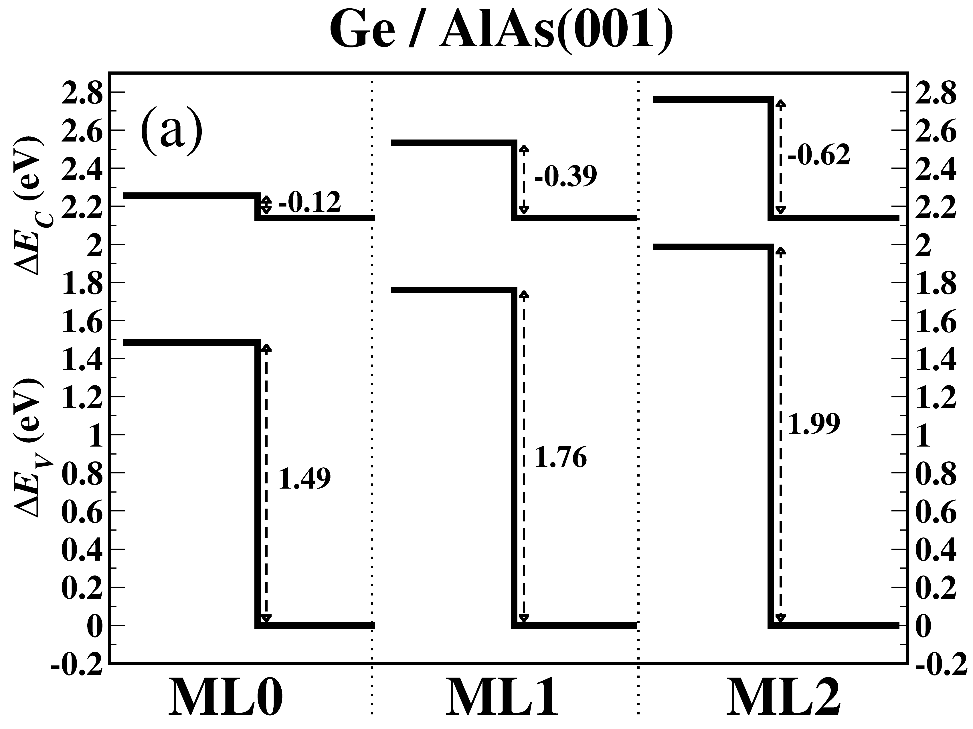
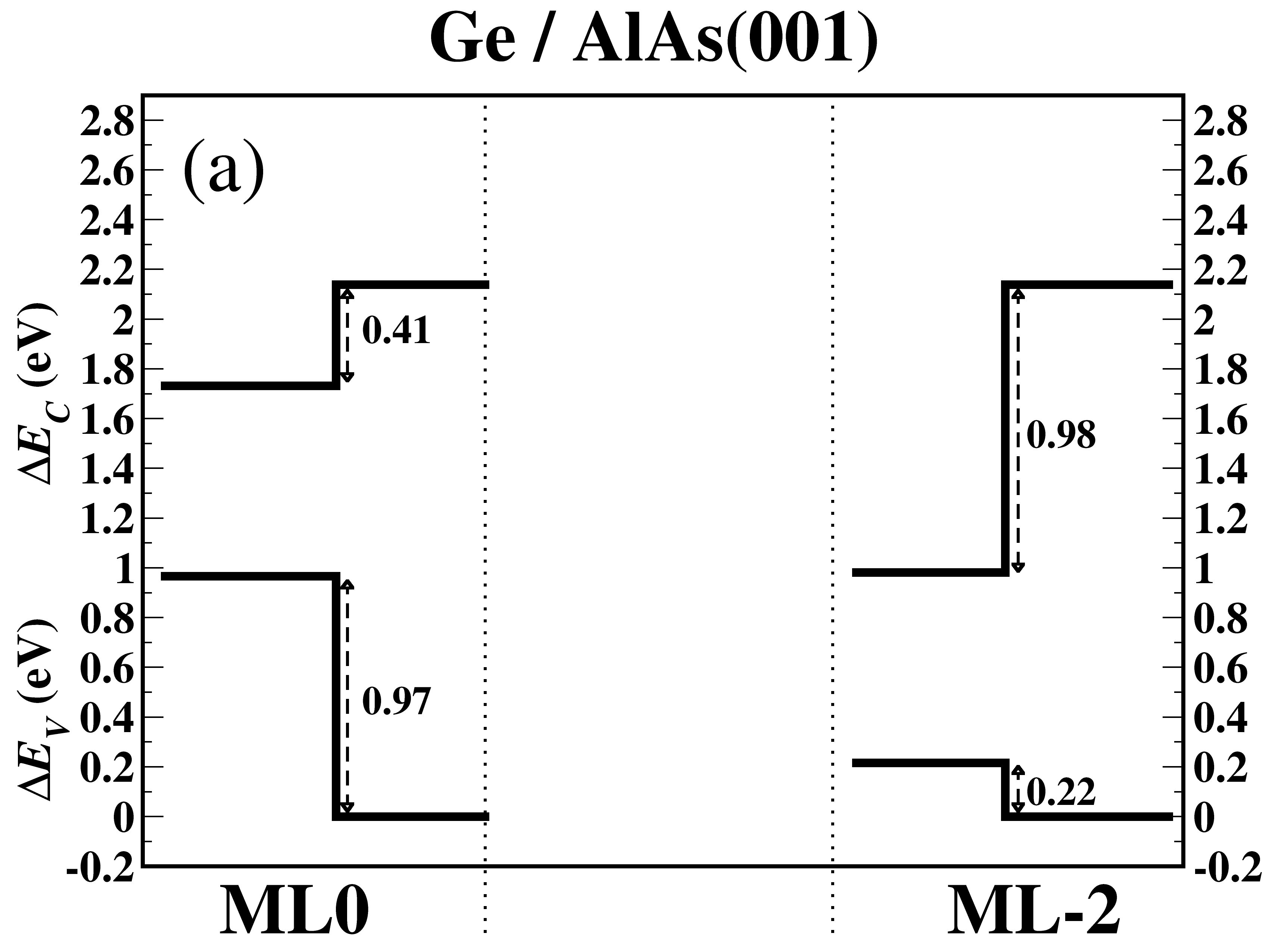
For example, consider the Ge/AlAs heterojunction with an abrupt interface in which the MIML consists of Ge and Al atoms (corresponding to the band offsets on the far left for = 0 and Ge = 0 in Fig. 3). This position of the MIML is referred to as ML0 (see right panel of Fig. 4). By using the VCA to linearly mix the atoms of ML0 and ML1 (see middle panel of Fig. 4), an approximation to an interfacial configuration involving mixed diffusion depths of Al atoms into the Ge slab can be achieved. For the case of Al atoms diffusing from ML0 to ML1, the stoichiometric balance between the monolayers required to maintain neutrality results in the relation
[Al0.5-−aGe0.5+a] = [AlaGe1−-a]
where [AlaGe1-a] is the composition of ML0/1, and is varied from 0 to 0.5. This is repeated for the case of Al atoms diffusing between ML1 and ML2, with used as the stoichiometry parameter instead of to avoid confusion. For the case of As atoms diffusing into Ge (see Sec. III.2.2), the stoichiometric relation is analogous, with Al sites being replaced by As. This procedure is also repeated for the case of Ge atoms diffusing into InxAl1-xAs (see Sec. III.2.3) which would more likely correspond to the scenario of a III-V slab grown on a Ge substrate.Chia et al. (2008) The stoichiometries of the endpoints (e.g. Al0.5Ge0.5 in ML0, ML1, or ML2, see Fig. 4) are calculated using explicit atomistic models (see Fig. 3) and compared to the corresponding VCA results for comparison.
As an additional assessment of the error associated with modeling the mixed layer stoichiometries with the VCA, the cluster expansion formalism is used to generate a special quasirandom structure (SQS)Wei et al. (1990) representation of the mixed monolayer with = 0.5. The ATAT codevan de Walle et al. (2002, 2013) is used to generate the periodic monolayer cell which exhibits multisite correlation functions for th nearest neighbor -atom clusters that match those of an infinite random 2 dimensional binary alloy with 50/50 composition, for up to = 2 and = 3. This monolayer SQS is used to compare to the ordered monolayer structures, and to the end-point VCA stoichiometries. This is done for Al diffusing into Ge, and for Ge diffusing into AlAs.
The results of these simulations are also compared to an analytical model based on a linear response theory for polar, heterovalent interfacesPeressi et al. (1998); Harrison et al. (1978). This model is described in Sec.III.3, and the results obtained from this model are shown as dashed lines in Figs. 5, 6, and 7.


| MIML | VBO | CBO | |
|---|---|---|---|
| Ge/AlAs(001) | |||
| ML0 | 0.97 | 0.41 | |
| ML1 | 0.74 (0.70) | 0.65 (0.61) | |
| ML2 | 0.46 (0.43) | 0.92 (0.89) | |
| -Ge/In0.25Al0.75As(001) | |||
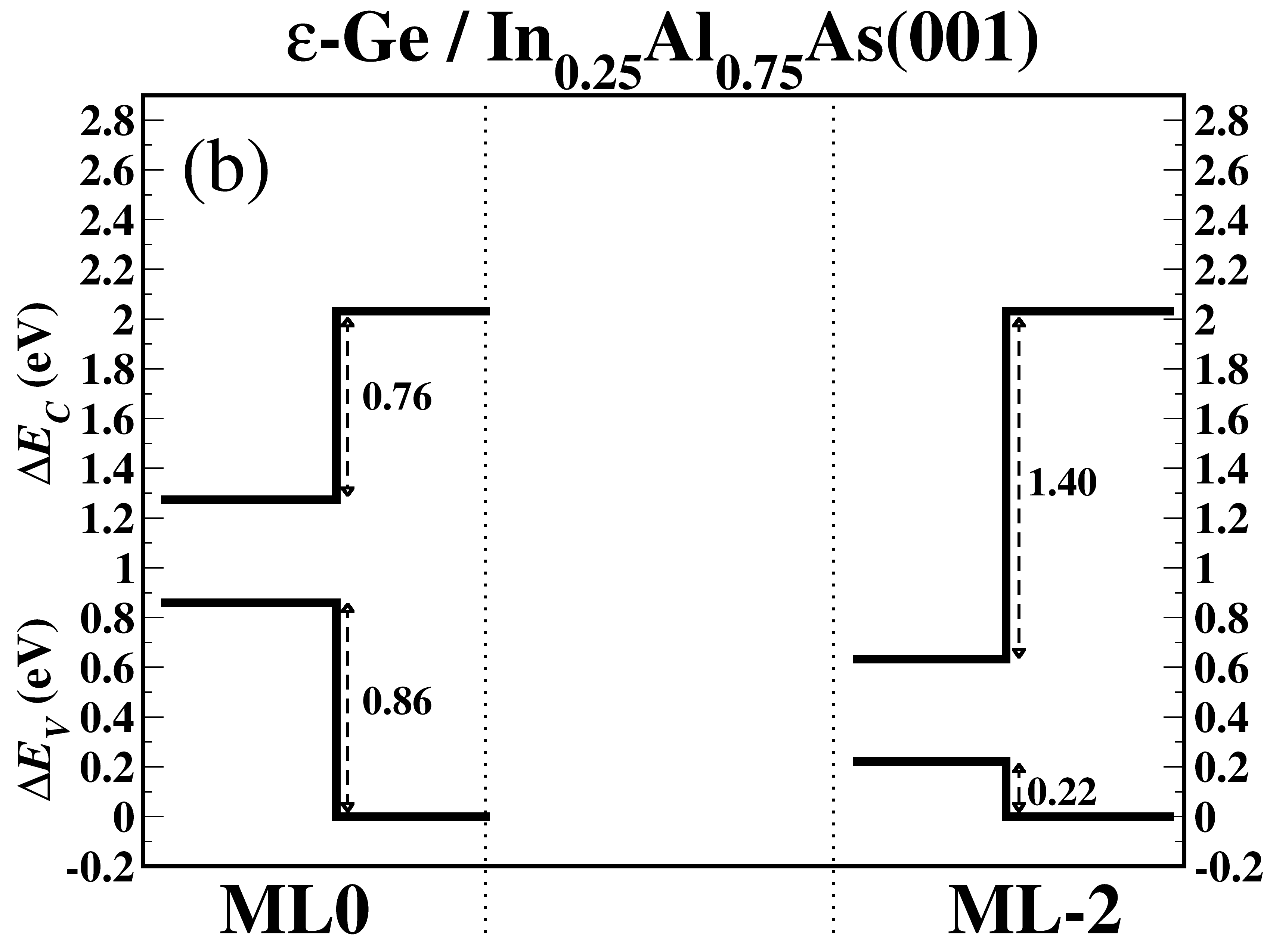
| ML0 | 0.86 | 0.75 | |
| ML1 | 0.72 (0.62) | 0.90 (0.80) | |
| ML2 | 0.48 (0.37) | 1.15 (1.04) |
III.2.1 InxAl1-x diffusion into Ge
For the case of Al atoms diffusing away from the Ge/AlAs(001) interface and into Ge, a linear change in the band offset is observed (panels (a) and (c) of Fig. 5). The band alignment is type-II for the case of the MIML residing at ML0 ([Al0.5Ge0.5]). Thus, for Ge films grown on Al-terminated AlAs(001), the valence (conduction) band edge of AlAs resides above (below) that of Ge, and for increasing diffusion depth of Al atoms into Ge the CBO becomes increasingly negative and the VBO increasingly positive. As a result, the band alignment is increasingly type-II over this range as a function of diffusion distance of Al. While a diffusion distance of up to 2 monolayers (corresponding to 3 Å) into Ge is particularly short, an increase in the band alignments of 0.50 eV (0.51 eV) is calculated for the explicit (VCA) models of the interface, which shows again the large sensitivity of band alignments to diffusion distance.
Turning to the lattice-mismatched interface -Ge/In0.25Al0.75As(001), a qualitatively similar movement of VBO and CBO with respect to diffusion distance of group-III (In and Al) atoms compared to Ge/AlAs(001) is calculated. The major difference compared to Ge/AlAs(001) is that the VBO for [(InAl)0.5Ge0.5] is small enough to yield a type-I band alignment. A type-I to type-II transition in the band alignment is observed as a function of diffusion distance for this case, with the CBO for [(InAl)0.5Ge0.5] being close to flat (0.01 eV) and [(InAl)0.5Ge0.5] exhibiting a type-II band offset (Fig. 5 (b)).
Thus for group-III cations diffusing across the interface and into -Ge, calculations show that this can have a large enough effect as to change the character of the band alignment relative to the abrupt interface, even for a very short diffusion distance of two monolayers. From the perspective of device physics, this finding has significant consequences. For example, for devices involving sandwiches of -Ge between In0.25Al0.75As(001) layers, the trapping of both electrons and holes (required for optically active recombination in optoelectronic applications) will be highly dependent on the diffusion depth of In and Al atoms into the -Ge layer. As the abrupt -Ge/In0.25Al0.75As(001) exhibits a type-I band alignment, these calculations show that atomic-scale abruptness of this interface is required to achieve significant optical recombination in the -Ge layer, which hinders the use of this particular interface in optical devices.
III.2.2 As diffusion into Ge
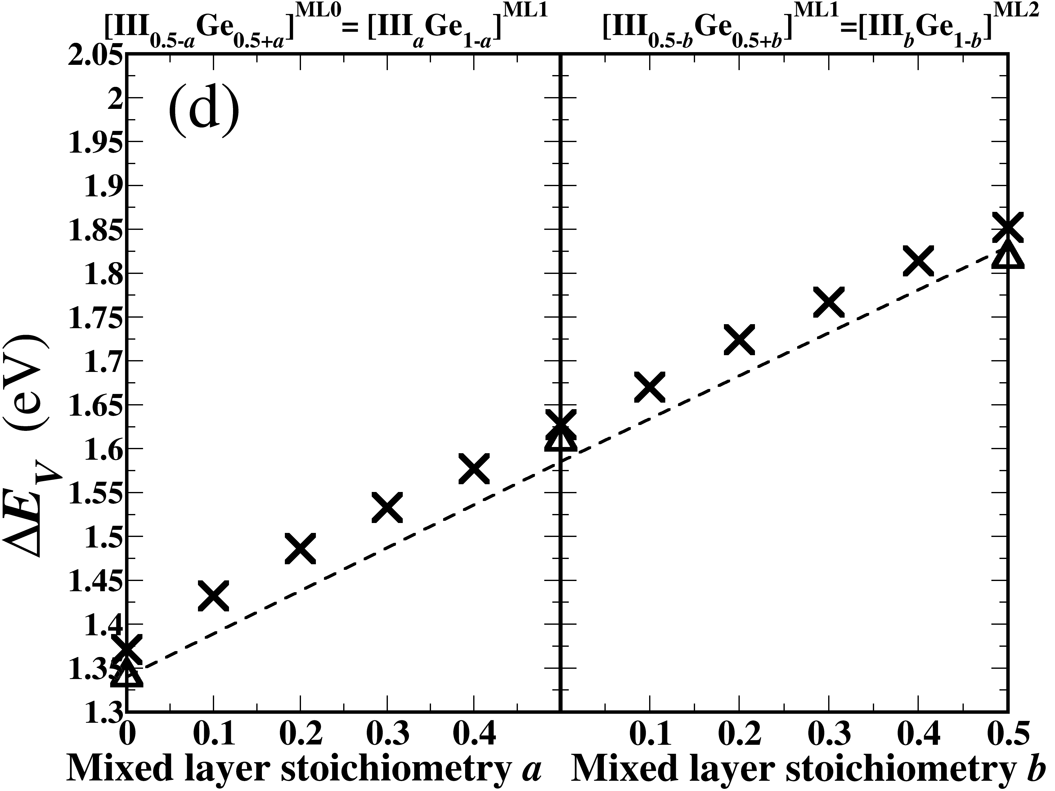
Calculations of band offsets were also performed for the case of As-terminated InxAl1-xAs, see Table 1.222For this case the As atoms of the MIML are moved into Ge in the manner described in sec. III.2, where the mixed layer stoichiometries are related by [As0.5-−aGe0.5+a] = [AsaGe1−-a] for As atoms diffusing from ML0 to ML1, and [As0.5-−bGe0.5+b] = [AsbGe1−-b] for As atoms diffusing from ML1 to ML2. The results show that band alignments are quite sensitive to diffusion distance into Ge. For the case of As atoms residing in ML1 ([As0.5Ge0.5]), the VBO is reduced by 0.23 eV compared to the abrupt (ML0) case, while the CBO correspondingly increases by 0.24 eV. For -Ge/In0.25Al0.75As(001), the VBO (CBO) decreases (increases) by 0.14 eV (0.15 eV). When As atoms have diffused to ML2 ([As0.5Ge0.5]), the BOs continue to move in the same direction, showing again a linear change with respect to interface stoichiometry as in the case of group-III diffusion into Ge (Sec. III.2.1), but with a slope of the opposite sign.
The VBO and CBO of Ge/AlAs for the [As0.5Ge0.5] case (0.46 eV and 0.92 eV, respectively) compare very well with recent BO measurements of the Ge/AlAs interface.Hudait et al. (2014) The calculated VBO (CBO) of -Ge/In0.25Al0.75As(001) for [As0.5Ge0.5] is 0.48 eV (1.15 eV). The latter BOs also compare well with unpublished experimental XPS measurements Clavel and Hudait of the band alignment of -Ge/In0.25Al0.75As(001).333The manuscript reporting this joint experimental and theoretical effort is currently under preparation. We therefore omit the band offset figures for this case (refer to Fig. 2 for the explicit models of [As0.5Ge0.5] in Ge/AlAs(001) and -Ge/In0.25Al0.75As(001)).
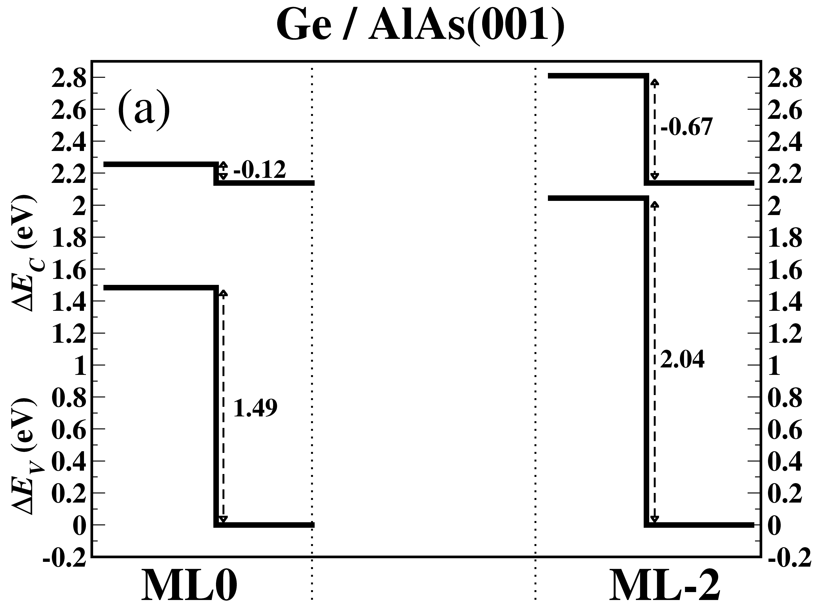
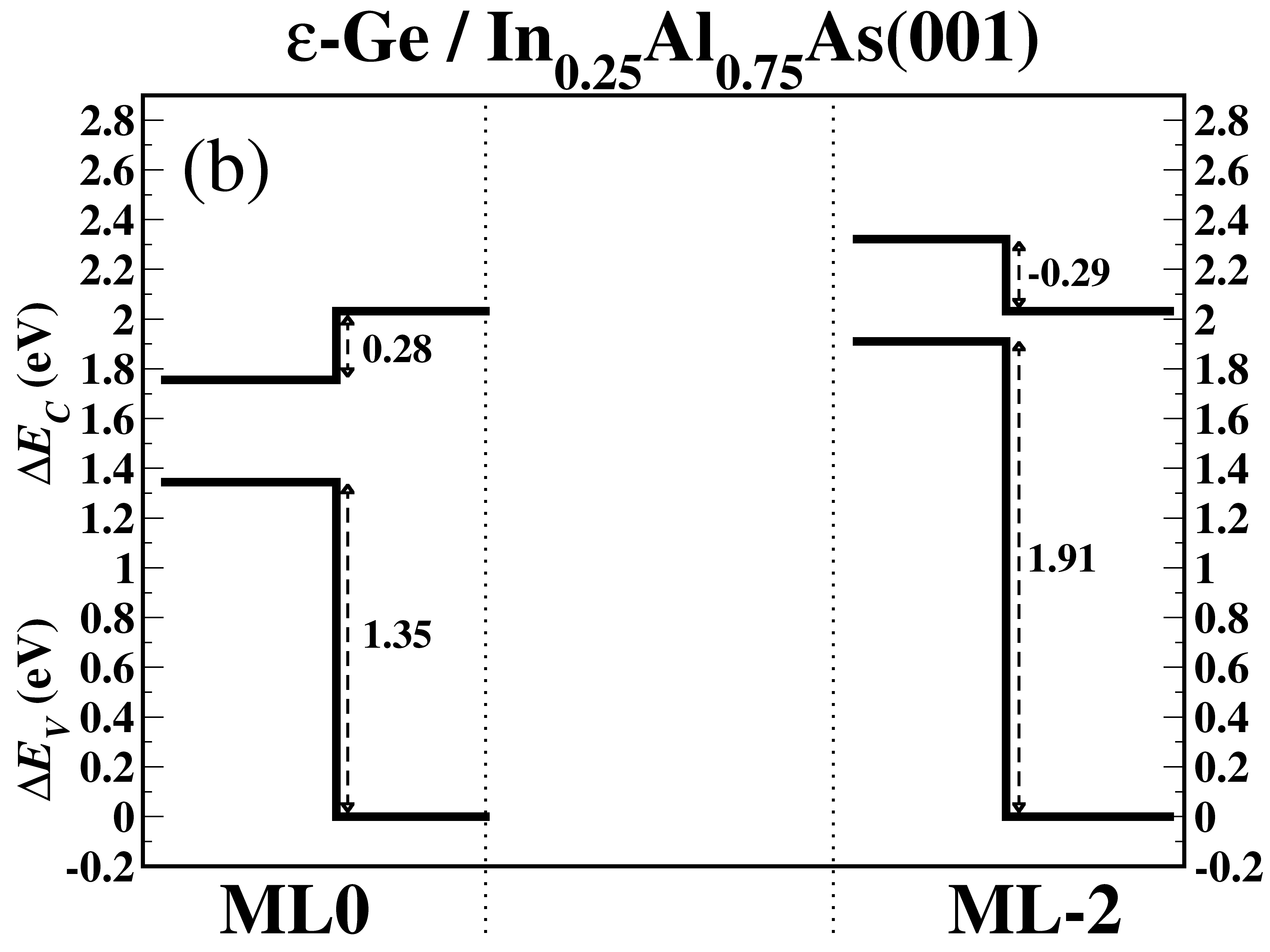
III.2.3 Ge diffusion into InxAl1-xAs
Due to the solid solubility of Ge in GaAs,Bosi and Attolini (2010) Ge diffusing through the interface towards the overlayer is a common observation in III-V/Ge(001) heterostructures (i.e. a III-Vs grown on Ge) such as GaAs/Ge(001). To a certain extent this diffusion and the overall interface quality can be controlled by growth conditions,Tanoto et al. (2006); Brammertz et al. (2008); Bosi et al. (2011); Sophia et al. (2015); Jia and Fitzgerald (2016) as well as by thin interlayers of AlAs (or alloys thereof) between GaAs and Ge.Chia et al. (2008); Li et al. (2013); Qi et al. (2014); Chen et al. (2016) The latter technique can decrease interdiffusion due to the large Al-As bond energy and yield heterostructures with very sharp interfaces between the III-V region and Ge. However diffusion cannot be completely suppressed and Ge diffusion distances of a few nm to tens of nm into the AlAs region can be observed.Chia et al. (2008) Many factors influence the investigation of heterostructures involving III-Vs grown on Ge, such as the potential of CMOS compatible monolithic integration of optical devicesFitzgerald et al. (1992); Chilukuri et al. (2007) where graded GeSi alloys act as a buffer between the III-V overlayer and the Si substrate. Also, high-quality III-V/Ge interfaces with a type-I BO could offer advantages for photovoltaic technologies.Bosi and Pelosi (2007); Guter et al. (2009); Qi et al. (2014) An understanding of the effects of Ge diffusion through the interface is imperative to the assessment of these potential applications.
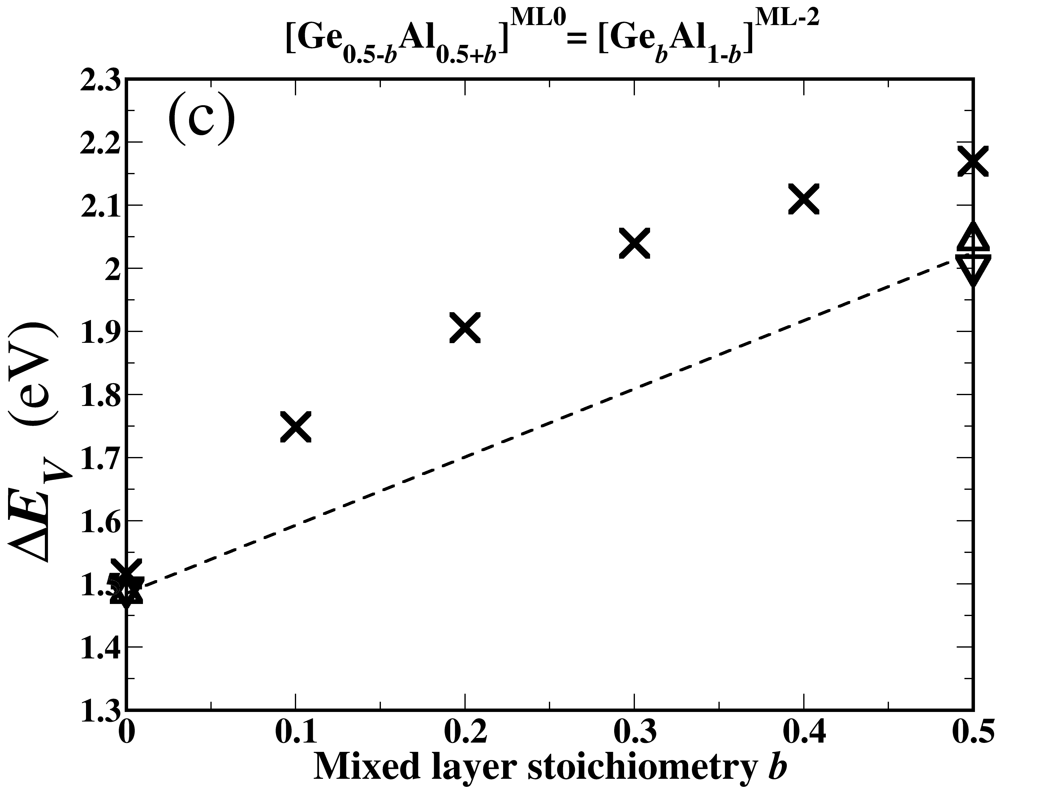
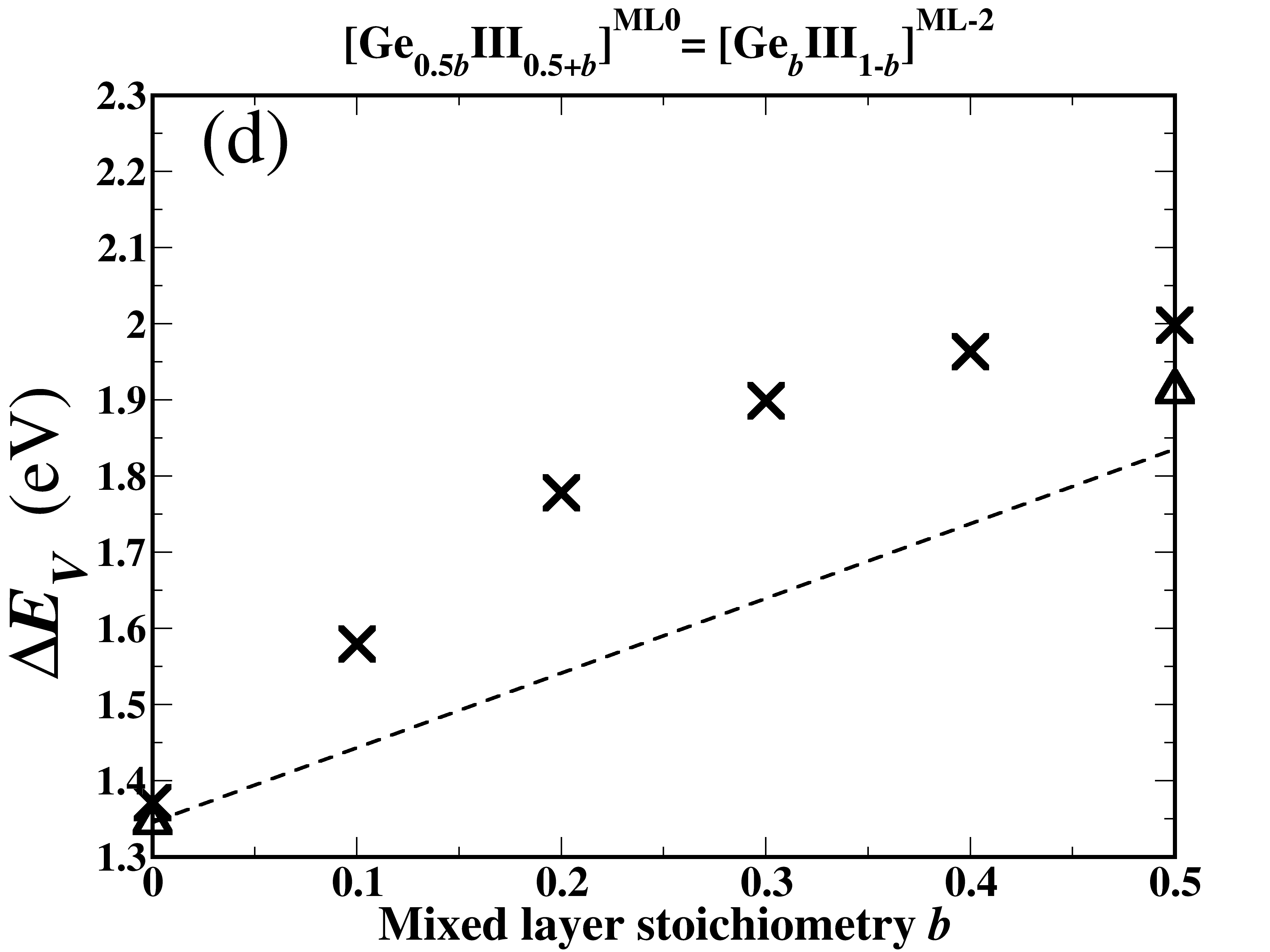
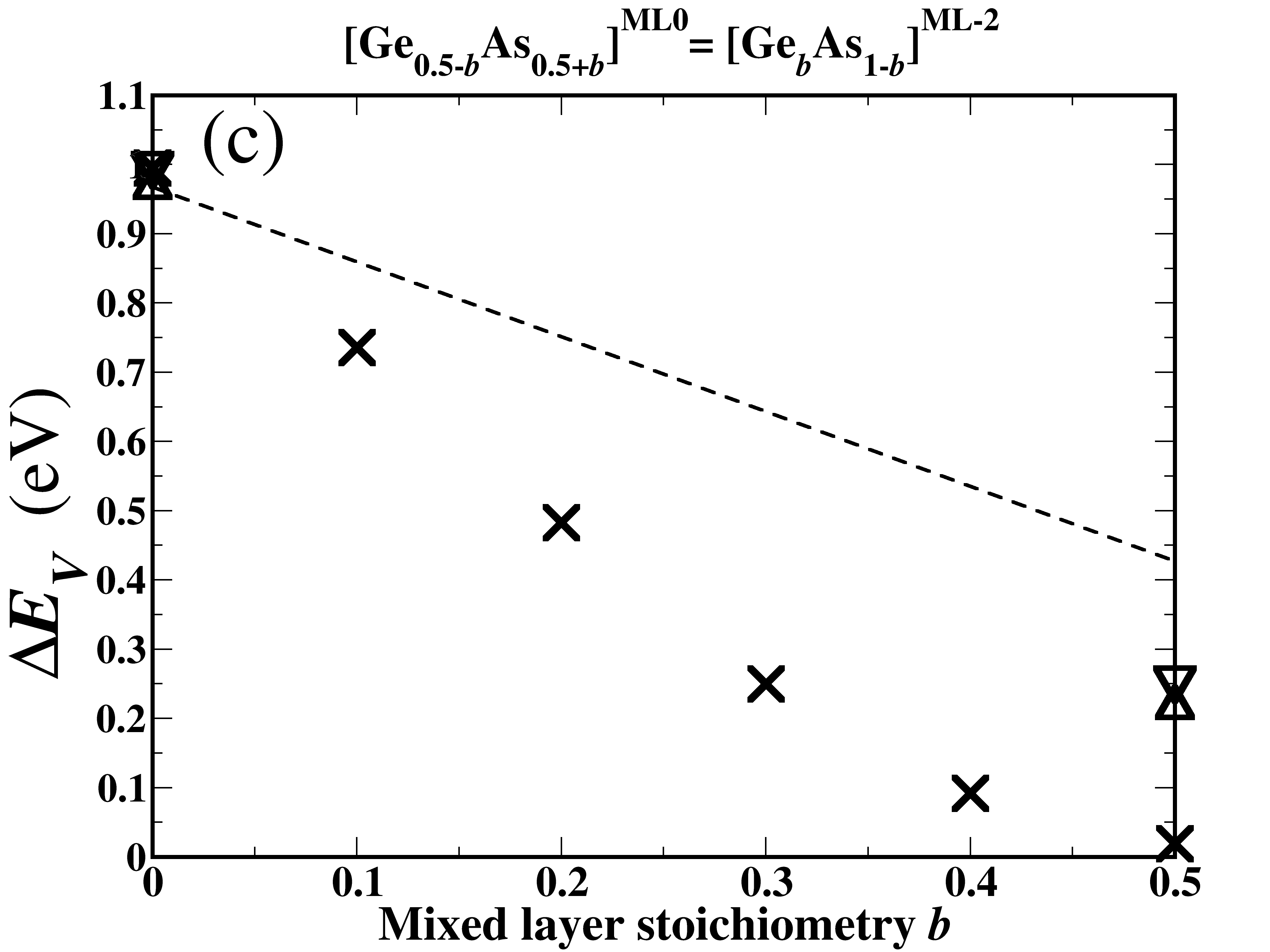
In this section, the effects of Ge diffusion into AlAs and In0.25Al0.75As on the BOs are studied for short diffusion distances. For the interface with In0.25Al0.75As, Ge is tensile strained to the III-V lattice constant, which models the top In0.25Al0.75As/-Ge interface of a confined -Ge region between a III-V overlayer and a III-V substrate, as is considered for optoelectronic applications.Pavarelli et al. (2013) Only the positions of Ge atoms which satisfy electron counting rulesPeressi et al. (1998); Martin (1980); Pashley (1989) for interfacial bonding are considered for this investigation, as this prevents the accumulation of an electric field across each slab which would result in unstable interface structures. For this reason, only the position of Ge atoms corresponding to the second monolayer away from the ML0 position and towards InxAl1-xAs (ML-2) is considered. In terms of the stoichiometric expression for the mixed layer as defined at the beginning of Sec. III.2, this corresponds to only [Geb(III)1−-b] ([Geb(As)1−-b]) being considered and compared to the abrupt [(III)0.5Ge0.5] ([As0.5Ge0.5]) interfaces for group-III (group-V) terminated InxAl1-xAs.
In contrast to the results of Secs. III.2.1 and III.2.2 involving InxAl1-xAs atoms diffusing into Ge, the band alignments in this section vary by a larger amount for a given diffusion distance. For group-III terminated InxAl1-xAs (see Fig. 6), an increase of 0.55 eV (0.56 eV) in the VBO is calculated for Ge diffusing to the ML-2 position in AlAs (In0.25Al0.75As). For AlAs, this almost results in a broken gap band alignment, as the CBE of AlAs is only 0.09 eV above the VBE of Ge. The CBE of In0.25Al0.75As(001) is also close to the VBE of -Ge, but with a larger separation (0.12 eV) compared to Ge-AlAs. Assuming continued linearity of the BOs as a function of diffusion distance, broken gap alignments are expected for these interfaces with a further diffusion of Ge into InxAl1-xAs.
This has important consequences for devices involving AlAs (with possibly small proportions of In) grown on Ge. At variance, movement of the VBO in the opposite direction is calculated for Ge atoms diffusing into AlAs (InxAl1-xAs) through an As terminated interface (see Fig. 7). In this case the VBO decreases by 0.75 eV (0.64 eV), which is qualitatively similar but significantly higher than the maximum VBO variation of 0.51 eV (0.38 eV) for As atoms diffusing through the Ge/AlAs(001) (-Ge/In0.25Al0.75As(001)) interface.
An apparent bowing of the VBO as a function of the mixed layer stoichiometry can be observed in panels (c) and (d) of Figs. 6 and 7, whereas this bowing effect is largely suppressed for the case of group-III atoms diffusing into Ge (Fig. 5 (c) and (d)). The bowing effect in Figs. 6 and 7 is likely an artifact of the VCA model of the interfacial region; the VCA cannot correctly capture local structural propertiesJaros (1985) which translates to errors in bond lengths and interlayer distances. These errors are exacerbated when the mixed monolayer, represented by the VCA, bonds to the neighboring ionic layers within the III-V crystal. The difference in bond lengths between III-V bonds and Ge-III/V bonds makes an important contribution to the local potential within the III-V slab and this contribution is missed in the VCA representation of the mixed layers for Ge diffusing into AlAs or In0.25Al0.75As. This causes larger errors for the intermediate values of which involve two types of VCA ‘atoms’ in the supercell, thus producing the bowing effect. For group-III atoms diffusing into Ge (see Sec. III.2.1), the VCA sites are now bonding to covalent rather than to ionic layers and the structural errors of the VCA are not so apparent.
The origin of the apparent bowing effect is further investigated by comparing the VCA results to explicit models of the mixed monolayer which are statistically representative of a 2 dimensional 50/50 random alloy (see panel (c) of Figs. 5, 6, and 7). For the cases of Ge diffusing into AlAs, the VBOs obtained by the SQS monolayer are much closer to those obtained by the ordered model, compared to those obtained by the VCA. This lends further credence to the possibility that the apparent bowing effect seen in the VCA VBOs is due to structural errors associated with the VCA, as opposed to a realistic effect. This is also the case for Al diffusing one monolayer into Ge (see Fig. 6), although for two monolayers of Al diffusion the VBO from the ordered model resides midway between the VCA and SQS result. In addition, the reduced bowing in this case (Fig. 6) indicates that the VCA is a better approximation for modeling mixed layers in materials with purely covalent bonding, compared to materials with some degree of ionic bonding.
III.2.4 Stability of diffused impurities
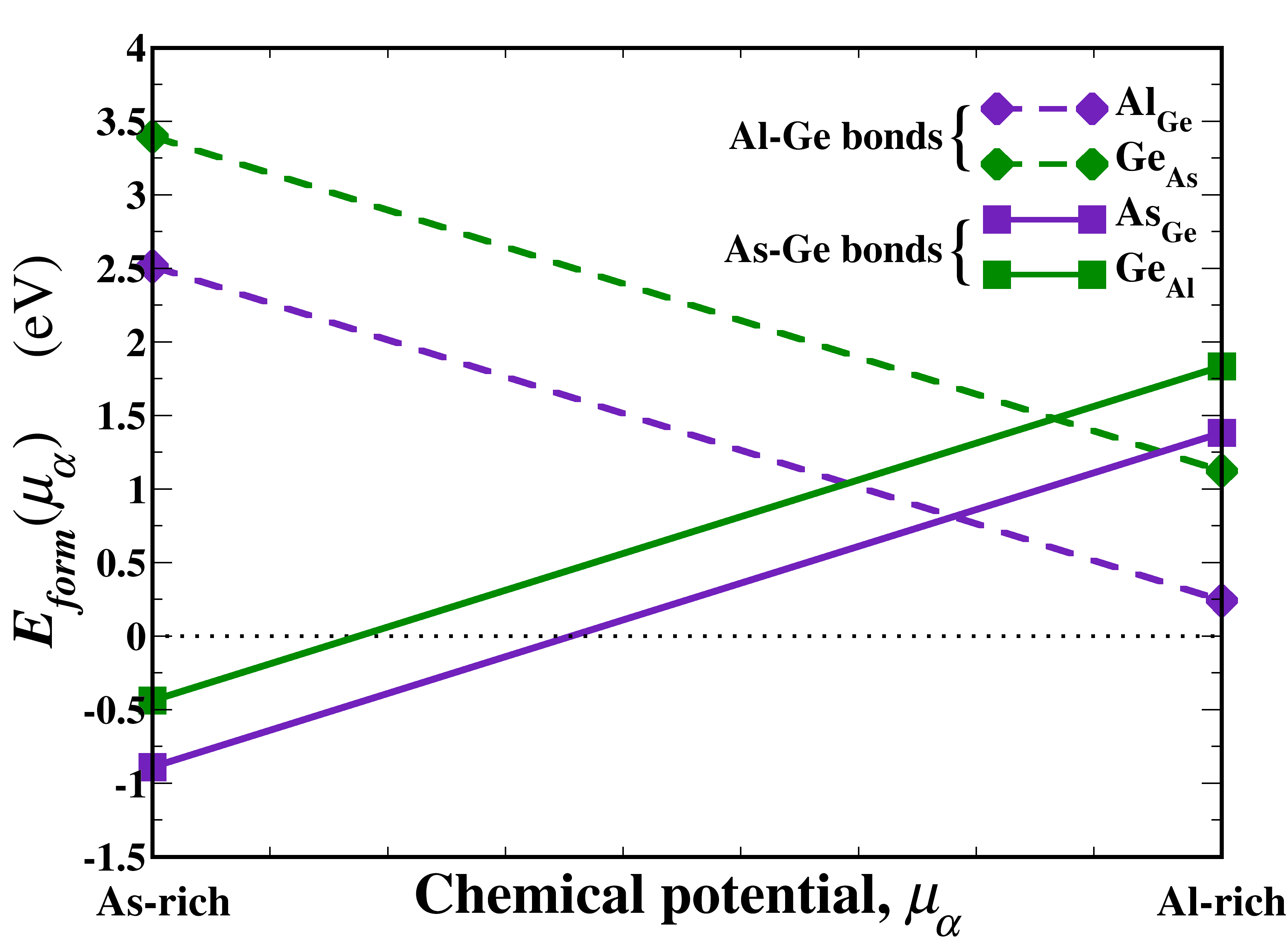
The formation energiesVan de Walle and Neugebauer (2004); Freysoldt et al. (2014); Zhang and Northrup (1991) of substitutional impurities were calculated in bulk cells in order to establish the relative stability (under conditions of thermodynamic equilibrium) of diffused impurities present in either Ge or AlAs after growth on top of either an AlAs substrate or a Ge substrate, respectively. Thus, the formation energetics establish, as a function of growth conditions, which diffused impurities are more likely to be present in either material after growth. The formation energies Eform(α) are plotted as a function of α for the each diffused impurity in Fig 8. For the majority of the range of α, the substitutional impurities which result in bonds between As and Ge have consistently lower formation energies than impurities corresponding to Al bonding to Ge.
In particular, these As-Ge bonding impurities have very low formation energies (note that negative formation energies correspond to impurities which form spontaneously under thermodynamic equilibrium, hence a kinetic process would be required to prevent their formation) under As-rich conditions. The latter has been used to realize high quality, abrupt interfaces,Clavel et al. (2015); Nguyen et al. (2015) hence we expect As-rich growth conditions to be favored for applications of these heterostructures. We also mention that our calculated heat of formation of AlAs is 2.27 eV, which overestimates the magnitude compared to the experimental value of 1.53 eVBerger (1996). While this affects the formation energetics, our purpose is simply to establish an approximate, qualitative picture of the relative stabilities, and the error (0.74 eV) does not reverse the relative stability of As-Ge bonding impurities and Al-Ge bonding impurities under As-rich growth conditions.
III.3 Analysis — Relation between band offsets and interface configurations
III.3.1 Electrostatic potential, charge density, and interface diffusion
The changes in band offsets presented in Sec. III.2 arise purely from changes in the term in Eqs. (1) and (2). This is equivalent to stating that the changes in band offsets arise purely from interfacial effects, specifically from changes in the interface dipole derived from the macroscopic average of the atomic potentials near the interface, (where the growth orientation is aligned to the direction). There is no contribution from bulk properties in the band alignment variations observed when comparing different interface structures (for a given group-III stoichiometry of InxAl1-xAs and strain state of Ge).
In general, atomic mixing affects the electrostatic potential line up by changing the charge density profile across the interface .Harrison et al. (1978); Brillson (2016) In fact, it can be shown that the electrostatic potential (Hartree potential + bare ionic ) step across the interface is given by
| (3) |
and it is equivalent to the interface dipole ( is the electronic charge, is the macroscopic average of ).Peressi et al. (1998) Then, modifications to the local charge density arising from changes to the bonding configuration near the interface can provide either an enhancement or reduction of the interface dipole,Peressi et al. (1998); McKinley et al. (1992) depending on the polarity of bonds to the diffusing species, and their diffusion depth. For this reason, the VBO and CBO variations can be explained by electrostatic considerations involving the effect of positions of IV-III and IV-V bonds on the local potential.
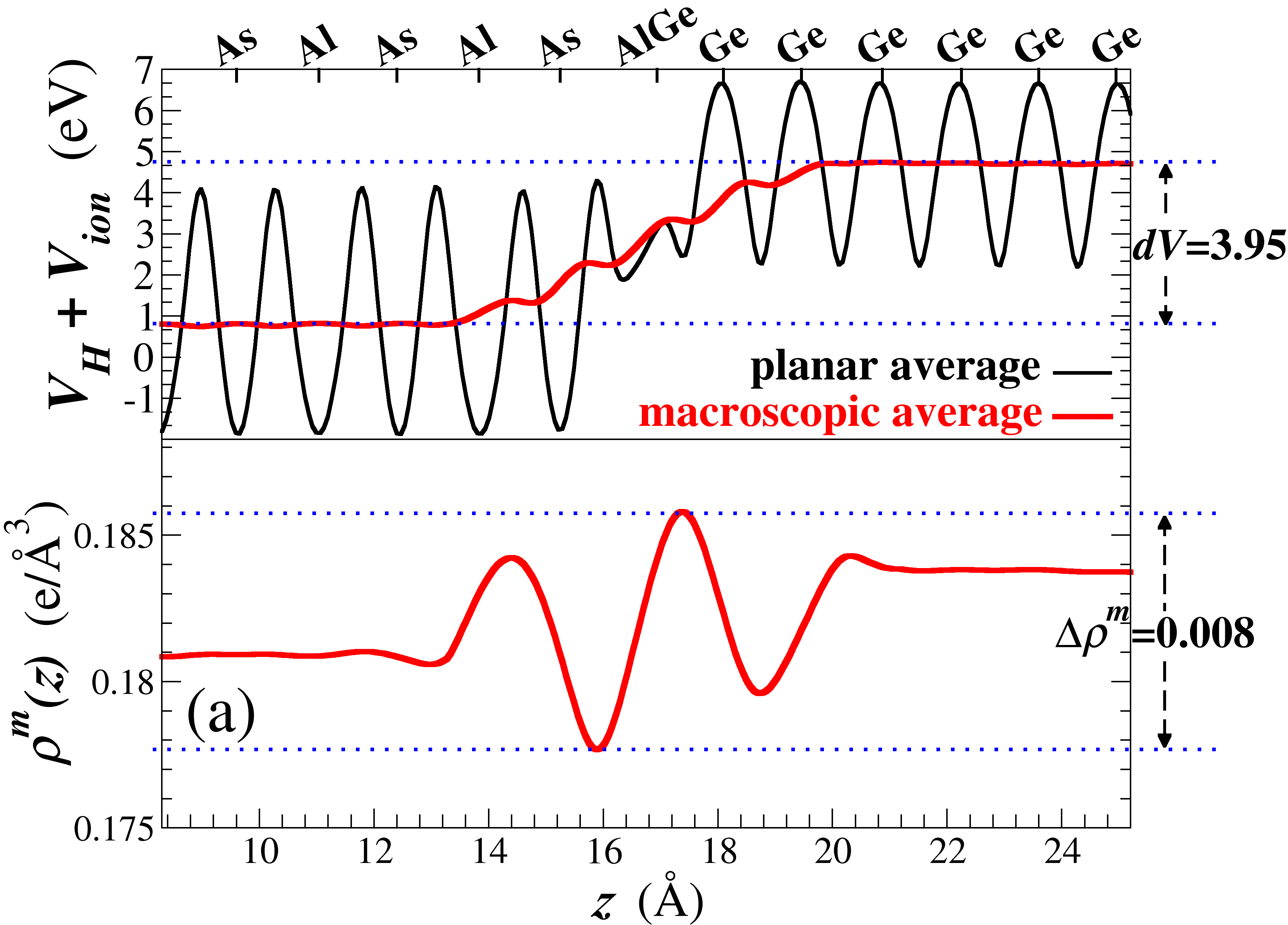
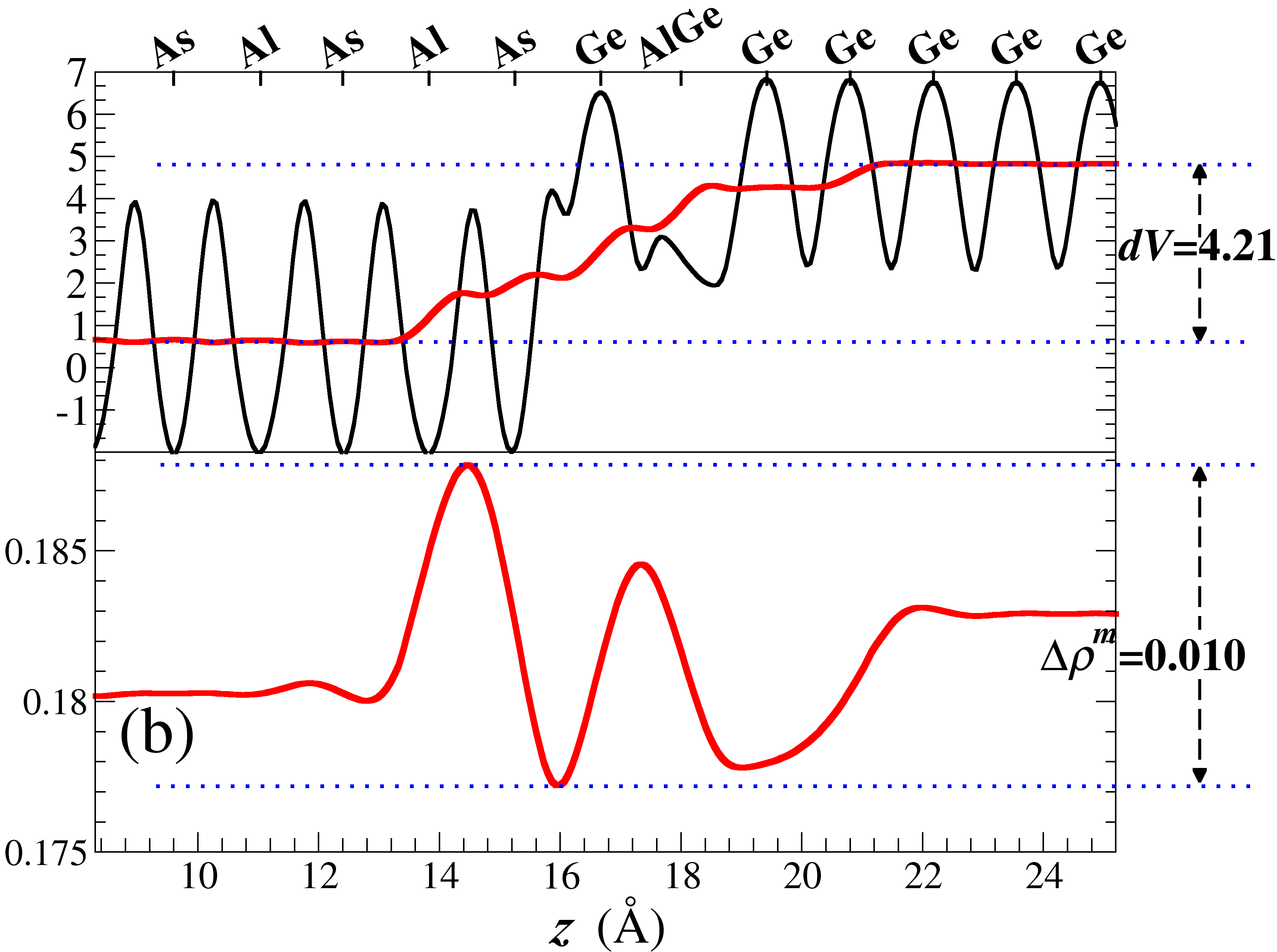
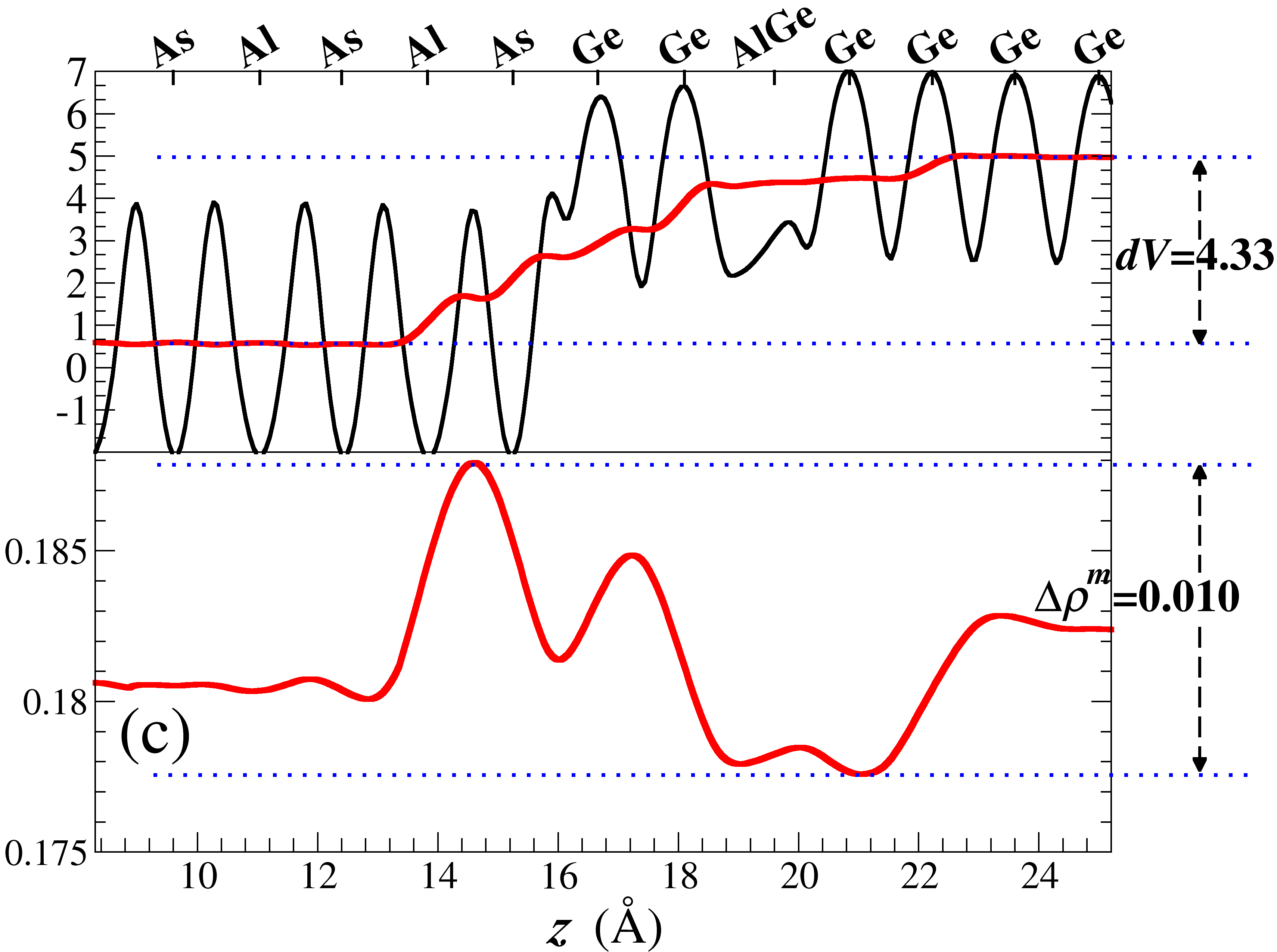
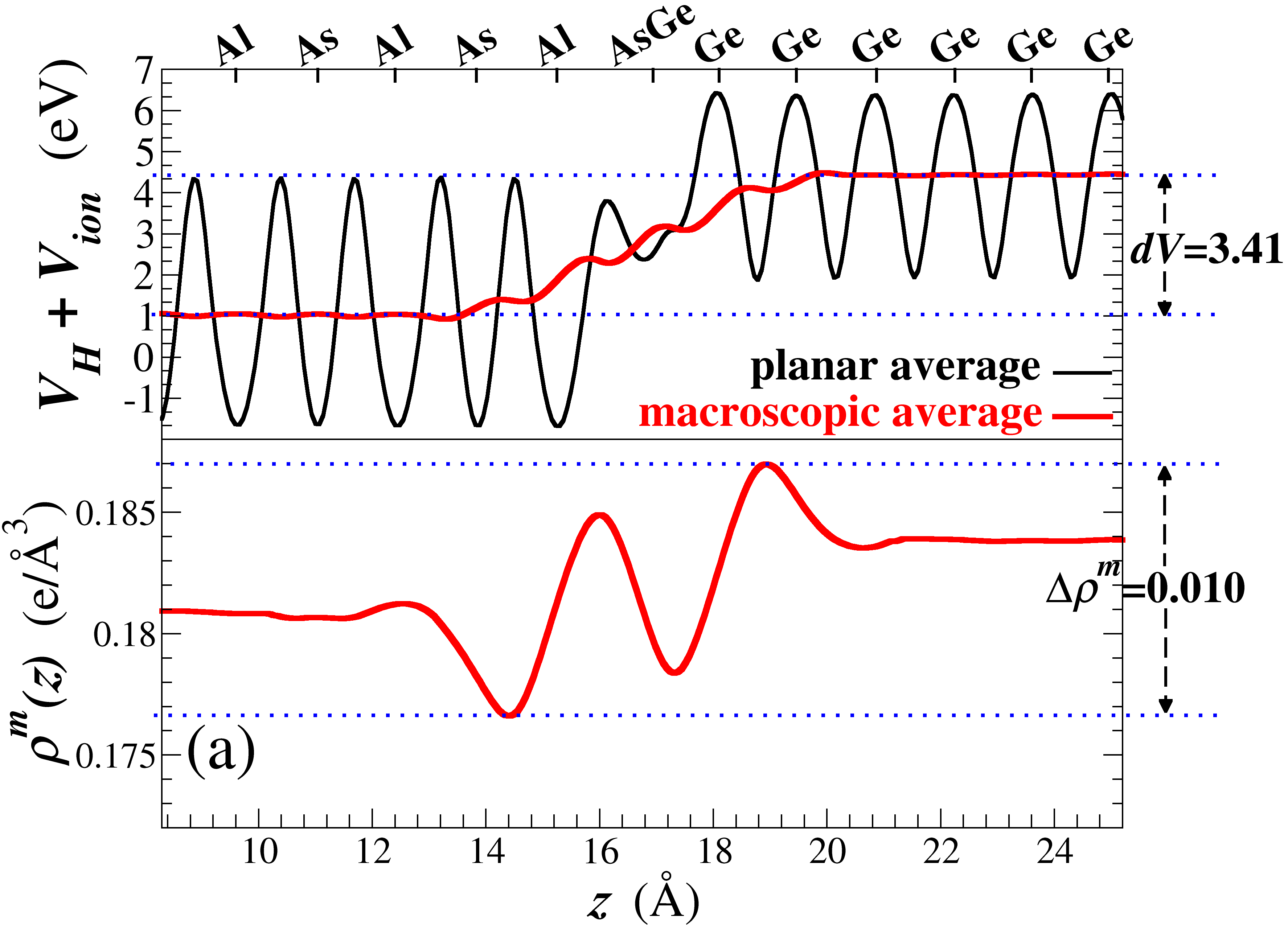
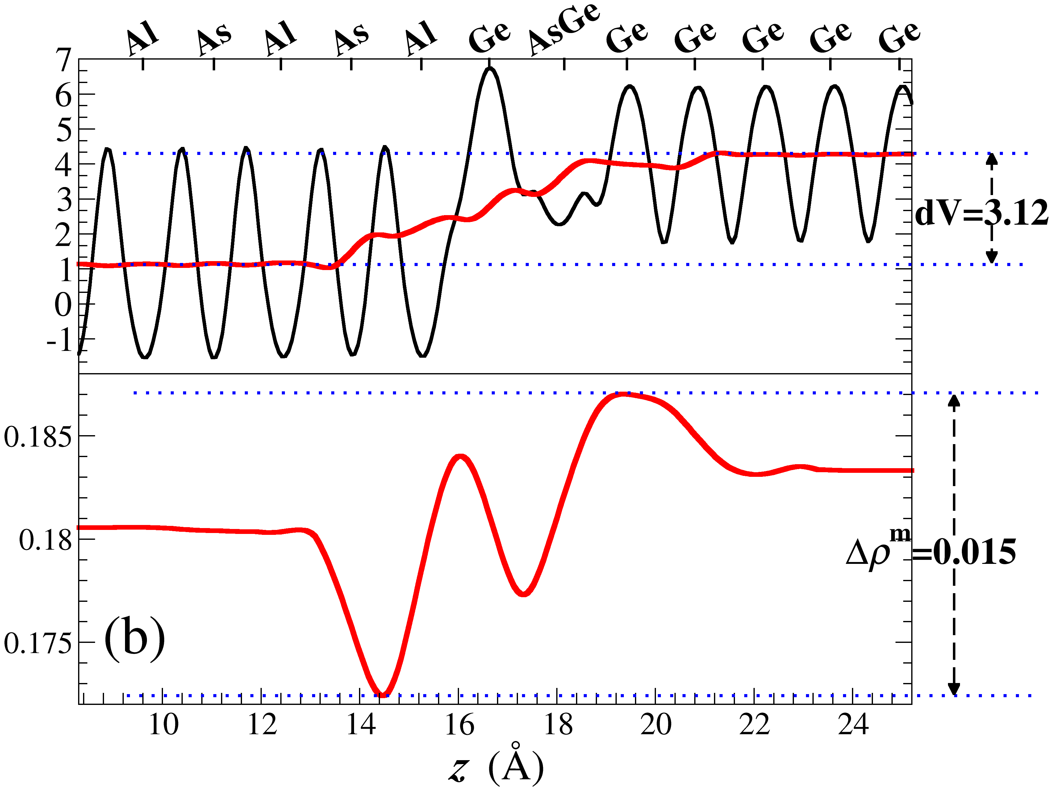
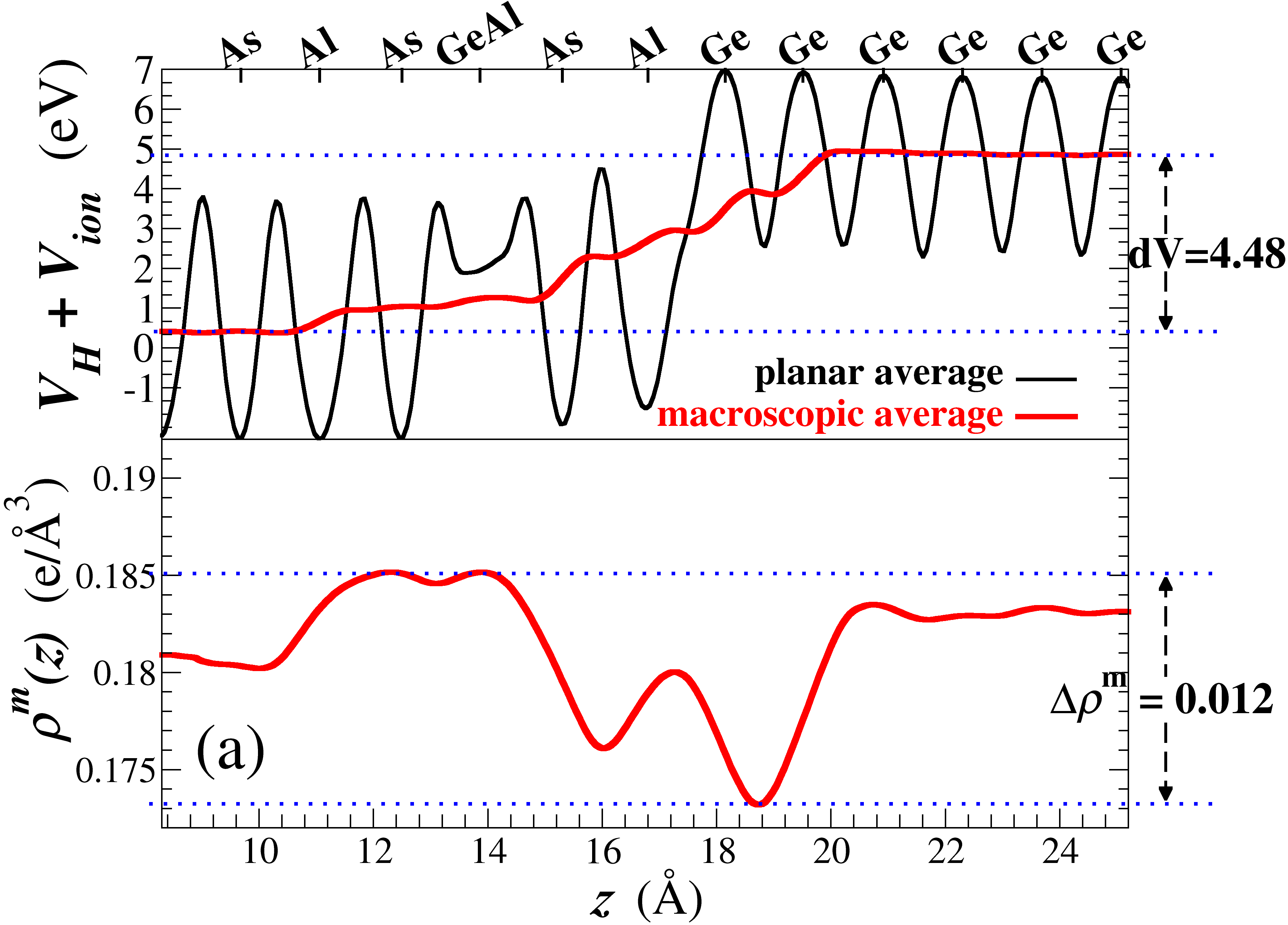
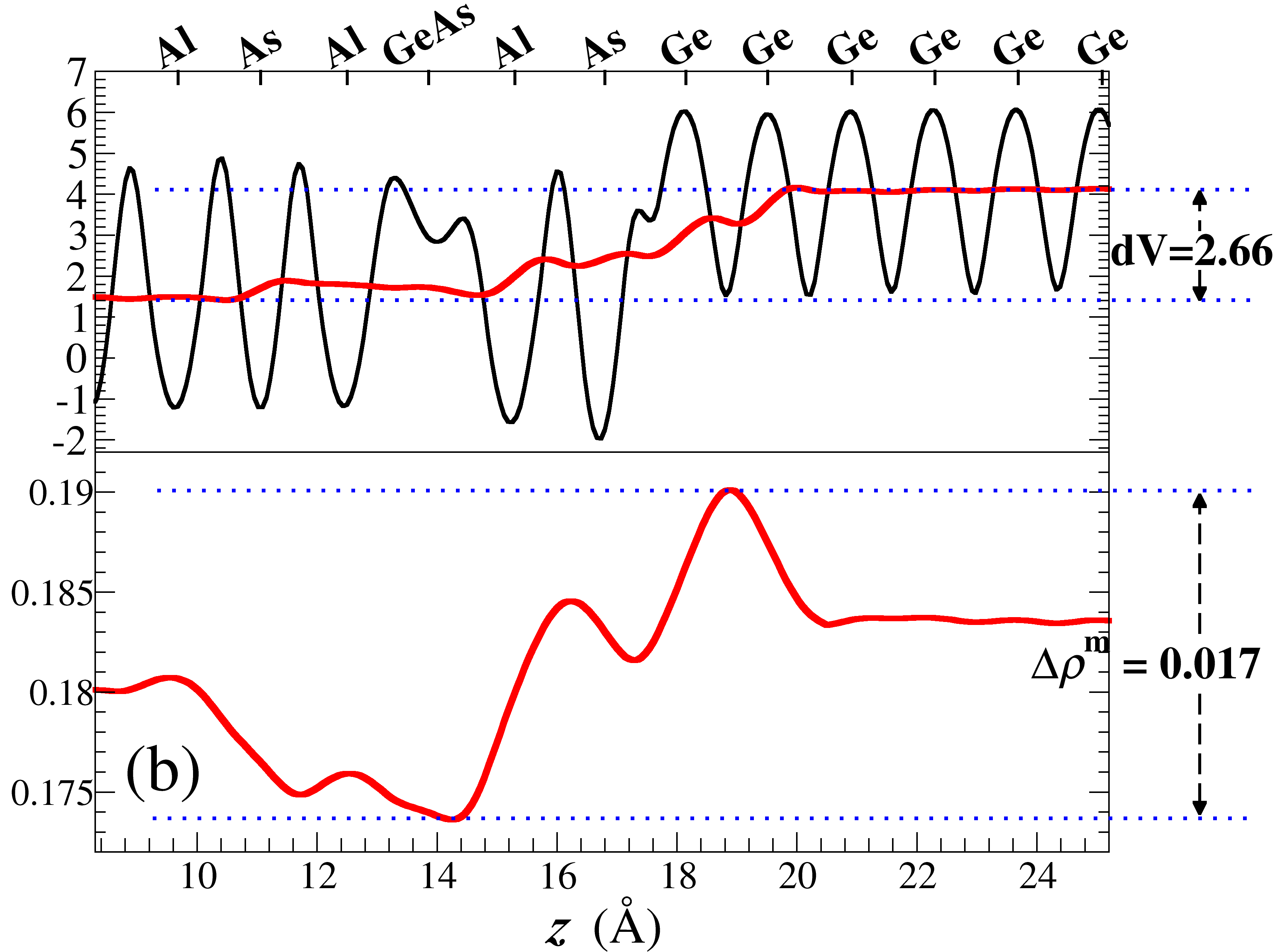
As a result of the valence charge carried by the diffusing atoms, we expect Ge-III bonds to contribute positively to as a function of diffusion distance of III atoms into Ge, and Ge-V bonds to contribute negatively to as a function of diffusion distance. This is indeed consistent with what we observe in Figs. 9 and 10. The former shows the planar and macroscopic averages of +, and for the explicit models of [Al0.5Ge0.5], [Al0.5Ge0.5], and [Al0.5Ge0.5] for the Ge-AlAs interface; the latter shows the same quantities for the [As0.5Ge0.5], [As0.5Ge0.5], and [As0.5Ge0.5] interface configurations of Ge/AlAs(001). It can be seen that as Ge-III (Ge-V) bonds move away from the abrupt interfacial layer and into Ge the step in the electrostatic potential increases (decreases), while the region over which charge transfer occurs widens. A similar conclusion is reached by plotting m and for the -Ge/In0.25Al0.75As(001) interfaces, which are not shown for brevity.
For Ge diffusing into InxAl1-xAs, (see Fig. 11) a larger change in relative to the abrupt interfaces is observed compared to the change in for Al and As atoms diffusing the same distance into Ge. This is not unexpected, given the relation between and Peressi et al. (1998); the variations in density across the interface m have a slightly larger amplitude for Ge diffusion into Al- or As-terminated AlAs compared to [Al0.5Ge0.5] or [As0.5Ge0.5] (compare to corresponding m values in Figs. 10 and 9), and this translates to a larger effect on the interface dipole for Ge diffusion.
III.3.2 Linear response theory applied to interface diffusion
Here we derive a simple model to describe the relationship between interface dipole and mixed layer stoichiometry across a heterovalent interface. We follow the linear response theory approachPeressi et al. (1998) put forward by Peressi et al. which is based on the model for polar interfaces proposed by Harrison Harrison et al. (1978). Within this approach, the interface is treated as a perturbation of a periodic reference crystal and the potential lineup consists of an isovalent (i.e. interface independent) and heterovalent terms = + . The is then obtained via the Poisson equation from the additional nuclear charges (carried by the perturbation) at each site.
For Al diffusing into Ge, we consider bulk Ge as the reference crystal. Hence, the additional nuclear charge per site along each monolayer across the interface is (schematically)
|
|
(4) |
where 0 is the mixed layer stoichiometry. The accumulated charge, found by summing adjacent sites from left to right, is then used to find the net contribution of interfacial charge to , which for Al diffusing into Ge becomes
| (5) |
where is the electron charge, the lattice constant of a GeAlAs alloy444Since Ge and AlAs are lattice matched this will be the bulk lattice constant of either Ge or AlAs and the dielectric constant of the same alloy obtained as an average of the Ge and the AlAs dielectric constant. This is similar for the case of As diffusing into Ge, but with the opposite sign,
| (6) |
For Ge diffusing into Al terminated AlAs, a similar line of reasoning results in the following interface contribution to the potential line up (again, is used here for the mixed stoichiometry instead of )
| (7) |
and for Ge diffusing into As terminated AlAs,
| (8) |
By considering as the average of the abrupt (ML0, = = = 0) cases for Al and As terminated AlAs, the isovalent contribution to the VBO follows from Eq. 1. for either Al(+) or As() terminated ML0 cases is then obtained from the difference - = , giving a value for the proportionality constant 0.27 eV in Ge/AlAs and 0.245 eV in -Ge/In0.25Al0.75As. The contribution due to diffusing away from the ML0 plane is then simply an additional 0.27 (0.245) eV per monolayer of diffusion through the Ge/AlAs (-Ge/In0.25Al0.75As) interface, which results in a linear relation between the VBO and stoichiometry of mixed layers containing diffused impurities.555We have also derived from first-principle by substituting in the expression the and values estimated from the LDA. In this case we obtained 0.29 eV and 0.27 eV respectively which would give comparable, though somewhat worse agreement with the values from the simulations.
Results show that this model agrees qualitatively with VBOs obtained from supercell calculations. We observe generally a better agreement between this model and calculations involving explicit interface configurations (non-VCA) than with VBOs obtained from the VCA representation of the interfaces (with the exception of Al diffusing 2 monolayers into Ge). The latter is particularly true for Ge atoms diffusing into (In)AlAs, which again shows the weakness of using VCA to represent mixed layers in a ionically bonded material.
IV Conclusions
First-principles calculations of valence and conduction band offsets have been performed using the DFT+ approach. The correction was applied to obtain accurate bulk bandgaps, while DFT within the LDA formulation provided the interfacial profile of the self-consistent potential from which the interface dipole can be derived. By varying the stoichiometry of monolayers near the interface using the VCA, the atomic diffusion away from the abrupt interfacial layer can be modeled. Within this approach, the term can be changed depending on the interlayer stoichiometry with a sensitivity large enough to, in some cases, change the character of the band alignment.
The results of this work are qualitatively consistent with the linear response theory developed for semiconductor interfaces,Resta et al. (1989) where for heterovalent interfaces the change in interface dipole (and hence the change in band offset) should be linear in the stoichiometries of mixed layers.Peressi et al. (1998); Bratina et al. (1994) We attribute the deviations from linearity showing an apparent bowing effect, especially for the cases of Ge diffusing into the III-V slab to the structural errors associated with the VCA.
The VCA has also been used to model the group-III alloy of the III-V slab, thus introducing a further error in the calculations of the band offsets. This error has been investigated in Ref. Greene-Diniz et al., 2016 for In0.5Ga0.5As. By comparing with the most accurate SQS, it was found that most of the error in the VCA resides in the indirect L-point satellite valley band gap, while the minimum error of the VCA corresponds to the direct -point band gap. As indicated by the early studies on SQS models, errors in band gaps obtained by averaging between the constituent binary materials generally follow the same trend for different III-V materials,Wei et al. (1990) hence the trends in VCA-errors should be transferable to InxAl1-xAs. For —the highest In content alloy studied in the present work—the band gap is direct at the -point, and we expect the least amount of error. While this error is not negligible (likely 0.1 eV), it is not large enough to change qualitative conclusions and trends of the present study.
Future studies will involve a wider range of explicit models of disordered configurations for the interface, in which various SQSZunger et al. (1990); Wei et al. (1990) representations of the interfacial layers will be compared against each other. This will shed more light on the band offset bowing effect and, by comparison, more accurately quantify the error in the band offsets when representing the mixed layer stoichiometries by the VCA. SQSs will also be used to model the group-III alloy of the III-V slab.
While the importance of the interface structure for heterovalent interfaces along with the associated departure from band offset transitivity seen for many isovalent interfaces is by now well-established, this work shows that variations in the interface stoichiometry can be enough to dramatically change the band alignment characteristics for the lattice (mis)matched (-)Ge/InxAl1-xAs(001) interface. Combining this with the experimentally validated band offsets achievable from DFT+ for conduction and valence band offsets, this work shows that due to variations in the interface dipole, both type-I and type-II band offsets should be observable for this interface depending on the details of the interface structure. Calculations of the formation energetics of diffused substitutional impurities indicate consistently greater stability of impurities which involve As bonding to Ge, for both materials comprising the interface. For the commonly used experimental approach of growing Ge on As-rich (nominally As-terminated) III-As substrates, from which atomically sharp interfaces can be achieved, these results are consistent with the observation of type-I band offsets for (-)Ge/InxAl1-xAs(001) for 0 0.25.
Acknowledgements.
The authors thank J. C. Abreu for providing the SQS models. The authors are grateful for helpful discussions with J. C. Abreu, F. Murphy-Armando, T. J. Ochalski, D. Saladukha, M. B. Clavel, M. K. Hudait, and J. Kohanoff. The authors acknowledge the use of computational facilities at the Atomistic Simulation Centre—Queen’s University Belfast. This work is financially supported by the Department for the Employment of Northern Ireland and InvestNI through the US-Ireland R&D partnership programme (USI-073).References
- Hudait et al. (2014) M. K. Hudait, M. Clavel, P. Goley, N. Jain, and Y. Zhu, Scientific Reports 4, 6964 (2014).
- Clavel et al. (2015) M. Clavel, P. Goley, N. Jain, Y. Zhu, and M. K. Hudait, IEEE Journal of the Electron Devices Society 3, 184 (2015).
- Nguyen et al. (2015) P. D. Nguyen, M. B. Clavel, P. S. Goley, J. S. Liu, N. P. Allen, L. J. Guido, and M. K. Hudait, IEEE Journal of the Electron Devices Society 3, 341 (2015).
- Ionescu and Riel (2014) A. M. Ionescu and H. Riel, Nature 8, 3136 (2014).
- Miller (2009) D. A. B. Miller, Proceedings of the IEEE 97, 1166 (2009).
- Assefa et al. (2010) S. Assefa, F. Xia, and Y. A. Vlasov, Nature 464, 80 (2010).
- Pavarelli et al. (2013) N. Pavarelli, T. J. Ochalski, F. Murphy-Armando, Y. Huo, M. Schmidt, G. Huyet, and J. S. Harris, Phys. Rev. Lett. 110, 177404 (2013).
- del Alamo (2011) J. A. del Alamo, Nature 479, 317 (2011).
- Ferain et al. (2011) I. Ferain, C. A. Colinge, and J.-P. Colinge, Nature 479, 310 (2011).
- Peressi et al. (1998) M. Peressi, N. Binggeli, and A. Baldereschi, Journal of Physics D: Applied Physics 31, 1273 (1998).
- Margaritondo (2012) G. Margaritondo, Electronic Structure of Semiconductor Heterojunctions, Perspectives in Condensed Matter Physics (Springer Netherlands, 2012).
- Agostini and Lamberti (2013) G. Agostini and C. Lamberti, Characterization of Semiconductor Heterostructures and Nanostructures (Elsevier Science, 2013).
- Brillson (2016) L. Brillson, An Essential Guide to Electronic Material Surfaces and Interfaces (Wiley, 2016).
- Van de Walle and Martin (1987) C. G. Van de Walle and R. M. Martin, Phys. Rev. B 35, 8154 (1987).
- Vandenberg et al. (1988) J. M. Vandenberg, M. B. Panish, H. Temkin, and R. A. Hamm, Applied Physics Letters 53, 1920 (1988).
- Christensen (1988) N. E. Christensen, Phys. Rev. B 38, 12687 (1988).
- Peressi et al. (1990) M. Peressi, S. Baroni, A. Baldereschi, and R. Resta, Phys. Rev. B 41, 12106 (1990).
- Hybertsen (1990) M. S. Hybertsen, Phys. Rev. Lett. 64, 555 (1990).
- Hybertsen (1991) M. S. Hybertsen, Applied Physics Letters 58, 1759 (1991).
- Harrison et al. (1978) W. A. Harrison, E. A. Kraut, J. R. Waldrop, and R. W. Grant, Phys. Rev. B 18, 4402 (1978).
- Waldrop and Grant (1979) J. R. Waldrop and R. W. Grant, Phys. Rev. Lett. 43, 1686 (1979).
- Kraut et al. (1980) E. A. Kraut, R. W. Grant, J. R. Waldrop, and S. P. Kowalczyk, Phys. Rev. Lett. 44, 1620 (1980).
- Biasiol et al. (1992) G. Biasiol, L. Sorba, G. Bratina, R. Nicolini, A. Franciosi, M. Peressi, S. Baroni, R. Resta, and A. Baldereschi, Phys. Rev. Lett. 69, 1283 (1992).
- Dahmen et al. (1993) M. Dahmen, U. Rau, M. Kawanaka, J. Sone, and J. H. Werner, Applied Physics Letters 62, 261 (1993).
- Volodin et al. (2014) V. A. Volodin, L. V. Sokolov, M. A. Pytyato, N. I. Petikov, M. Stoffel, H. Rinnert, and M. Vergnat, Journal of Applied Physics 115, 053518 (2014).
- Martin (1980) R. M. Martin, Journal of Vacuum Science and Technology 17, 978 (1980).
- Kunc and Martin (1981) K. Kunc and R. M. Martin, Phys. Rev. B 24, 3445 (1981).
- Peressi et al. (1991) M. Peressi, S. Baroni, R. Resta, and A. Baldereschi, Phys. Rev. B 43, 7347 (1991).
- Franciosi et al. (1993) A. Franciosi, L. Sorba, G. Bratina, and G. Biasiol, Journal of Vacuum Science & Technology B: Microelectronics and Nanometer Structures Processing, Measurement, and Phenomena 11, 1628 (1993).
- Resta et al. (1989) R. Resta, S. Baroni, and A. Baldereschi, Superlattices and Microstructures 6, 31 (1989).
- Chason and Guduru (2016) E. Chason and P. R. Guduru, Journal of Applied Physics 119, 191101 (2016).
- Liang and Bowers (2010) D. Liang and J. E. Bowers, Nature Photonics 4, 511 (2010).
- Perdew and Zunger (1981) J. P. Perdew and A. Zunger, Phys. Rev. B 23, 5048 (1981).
- Perdew and Wang (1992) J. P. Perdew and Y. Wang, Phys. Rev. B 45, 13244 (1992).
- Troullier and Martins (1991) N. Troullier and J. L. Martins, Phys. Rev. B 43, 1993 (1991).
- Giannozzi et al. (2009) P. Giannozzi, S. Baroni, N. Bonini, M. Calandra, R. Car, C. Cavazzoni, D. Ceresoli, G. L. Chiarotti, M. Cococcioni, I. Dabo, A. D. Corso, S. de Gironcoli, S. Fabris, G. Fratesi, R. Gebauer, U. Gerstmann, C. Gougoussis, A. Kokalj, M. Lazzeri, L. Martin-Samos, N. Marzari, F. Mauri, R. Mazzarello, S. Paolini, A. Pasquarello, L. Paulatto, C. Sbraccia, S. Scandolo, G. Sclauzero, A. P. Seitsonen, A. Smogunov, P. Umari, and R. M. Wentzcovitch, Journal of Physics: Condensed Matter 21, 395502 (2009).
- Louie et al. (1982) S. G. Louie, S. Froyen, and M. L. Cohen, Phys. Rev. B 26, 1738 (1982).
- Monkhorst and Pack (1976) H. J. Monkhorst and J. D. Pack, Phys. Rev. B 13, 5188 (1976).
- Baldereschi et al. (1988) A. Baldereschi, S. Baroni, and R. Resta, Phys. Rev. Lett. 61, 734 (1988).
- Giantomassi et al. (2011) M. Giantomassi, M. Stankovski, R. Shaltaf, M. Grüning, F. Bruneval, P. Rinke, and G.-M. Rignanese, physica status solidi (b) 248, 275 (2011).
- Van de Walle and Neugebauer (2004) C. G. Van de Walle and J. Neugebauer, Journal of Applied Physics 95, 3851 (2004).
- Freysoldt et al. (2014) C. Freysoldt, B. Grabowski, T. Hickel, J. Neugebauer, G. Kresse, A. Janotti, and C. G. Van de Walle, Rev. Mod. Phys. 86, 253 (2014).
- Note (1) We do not consider InxAl1-xAs with 0 for this purpose due to the inaccurate bond lengths resulting from the VCA approach which would lead to inaccurate impurity-host bonding energies.
- Zhang and Northrup (1991) S. B. Zhang and J. E. Northrup, Phys. Rev. Lett. 67, 2339 (1991).
- Bylander and Kleinman (1990) D. M. Bylander and L. Kleinman, Phys. Rev. B 41, 3509 (1990).
- Perdew et al. (1982) J. P. Perdew, R. G. Parr, M. Levy, and J. L. Balduz, Phys. Rev. Lett. 49, 1691 (1982).
- Sham and Schlüter (1985) L. J. Sham and M. Schlüter, Phys. Rev. B 32, 3883 (1985).
- Godby et al. (1988) R. W. Godby, M. Schlüter, and L. J. Sham, Phys. Rev. B 37, 10159 (1988).
- Hedin (1965) L. Hedin, Phys. Rev. 139, A796 (1965).
- Aryasetiawan and Gunnarsson (1998) Aryasetiawan and Gunnarsson, Reports on Progress in Physics 61, 237 (1998).
- Hybertsen and Louie (1986) M. S. Hybertsen and S. G. Louie, Phys. Rev. B 34, 5390 (1986).
- Grüning et al. (2010) M. Grüning, R. Shaltaf, and G.-M. Rignanese, Phys. Rev. B 81, 035330 (2010).
- Madelung (2004) O. Madelung, Semiconductors: Data Handbook (Springer Berlin Heidelberg, 2004).
- Cheng et al. (2012) Y. Cheng, C. Chia, Y. Chai, and D. Chi, Thin Solid Films 522, 340 (2012).
- Maeda et al. (1995) T. Maeda, H. Tanaka, M. Takikawa, and K. Kasai, Journal of Crystal Growth 150, 649 (1995).
- Maeda and Tanaka (1999) T. Maeda and H. Tanaka, Journal of Crystal Growth 201-202, 194 (1999).
- Chia et al. (2008) C. K. Chia, J. R. Dong, D. Z. Chi, A. Sridhara, A. S. W. Wong, M. Suryana, G. K. Dalapati, S. J. Chua, and S. J. Lee, Applied Physics Letters 92, 141905 (2008).
- Wei et al. (1990) S.-H. Wei, L. G. Ferreira, J. E. Bernard, and A. Zunger, Phys. Rev. B 42, 9622 (1990).
- van de Walle et al. (2002) A. van de Walle, M. D. Asta, and G. Ceder, Calphad 26, 539 (2002).
- van de Walle et al. (2013) A. van de Walle, P. Tiwary, M. M. de Jong, D. L. Olmsted, M. D. Asta, A. Dick, D. Shin, Y. Wang, L.-Q. Chen, and Z.-K. Liu, Calphad 42, 13 (2013).
- Note (2) For this case the As atoms of the MIML are moved into Ge in the manner described in sec. III.2, where the mixed layer stoichiometries are related by [As0.5-−aGe0.5+a] = [AsaGe1−-a] for As atoms diffusing from ML0 to ML1, and [As0.5-−bGe0.5+b] = [AsbGe1−-b] for As atoms diffusing from ML1 to ML2.
- (62) M. Clavel and M. K. Hudait, private communication.
- Note (3) The manuscript reporting this joint experimental and theoretical effort is currently under preparation. We therefore omit the band offset figures for this case (refer to Fig. 2 for the explicit models of [As0.5Ge0.5] in Ge/AlAs(001) and -Ge/In0.25Al0.75As(001)).
- Bosi and Attolini (2010) M. Bosi and G. Attolini, Progress in Crystal Growth and Characterization of Materials 56, 146 (2010).
- Tanoto et al. (2006) H. Tanoto, S. F. Yoon, W. K. Loke, E. A. Fitzgerald, C. Dohrman, B. Narayanan, M. T. Doan, and C. H. Tung, Journal of Vacuum Science & Technology B: Microelectronics and Nanometer Structures Processing, Measurement, and Phenomena 24, 152 (2006).
- Brammertz et al. (2008) G. Brammertz, M. Caymax, M. Meuris, M. Heyns, Y. Mols, S. Degroote, and M. Leys, Thin Solid Films 517, 148 (2008).
- Bosi et al. (2011) M. Bosi, G. Attolini, C. Ferrari, C. Frigeri, M. Calicchio, F. Rossi, K. Vad, A. Csik, and Z. Zolnai, Journal of Crystal Growth 318, 367 (2011).
- Sophia et al. (2015) P. J. Sophia, G. Attolini, M. Bosi, E. Buffagni, C. Ferrari, C. Frigeri, K. Vad, A. Csik, V. Takáts, and Z. Zolnai, ECS Journal of Solid State Science and Technology 4, 53 (2015).
- Jia and Fitzgerald (2016) R. Jia and E. A. Fitzgerald, Journal of Crystal Growth 435, 50 (2016).
- Li et al. (2013) S. Li, Q. Chen, J. Zhang, H. Chen, W. Xu, H. Xiong, Z. Wu, Y. Fang, C. Chen, and Y. Tian, Journal of Vacuum Science & Technology B, Nanotechnology and Microelectronics: Materials, Processing, Measurement, and Phenomena 31, 041202 (2013).
- Qi et al. (2014) M. Qi, C. A. Stephenson, V. Protasenko, W. A. O’Brien, A. Mintairov, H. G. Xing, and M. A. Wistey, Applied Physics Letters 104, 073113 (2014).
- Chen et al. (2016) J. X. Chen, W. He, S. P. Jia, D. S. Jiang, S. L. Lu, L. F. Bian, and H. Yang, Journal of Electronic Materials 45, 853 (2016).
- Fitzgerald et al. (1992) E. A. Fitzgerald, Y. Xie, D. Monroe, P. J. Silverman, J. M. Kuo, A. R. Kortan, F. A. Thiel, and B. E. Weir, Journal of Vacuum Science & Technology B: Microelectronics and Nanometer Structures Processing, Measurement, and Phenomena 10, 1807 (1992).
- Chilukuri et al. (2007) K. Chilukuri, M. J. Mori, C. L. Dohrman, and E. A. Fitzgerald, Semiconductor Science and Technology 22, 29 (2007).
- Bosi and Pelosi (2007) M. Bosi and C. Pelosi, Progress in Photovoltaics: Research and Applications 15, 51 (2007).
- Guter et al. (2009) W. Guter, J. Schöne, S. P. Philipps, M. Steiner, G. Siefer, A. Wekkeli, E. Welser, E. Oliva, A. W. Bett, and F. Dimroth, Applied Physics Letters 94, 223504 (2009).
- Pashley (1989) M. D. Pashley, Phys. Rev. B 40, 10481 (1989).
- Jaros (1985) M. Jaros, Reports on Progress in Physics 48, 1091 (1985).
- Berger (1996) L. Berger, Semiconductor Materials (Taylor & Francis, 1996).
- McKinley et al. (1992) J. McKinley, Y. Hwu, B. Koltenbah, G. Margaritondo, S. Baroni, and R. Resta, Applied Surface Science 56-58, 762 (1992).
- Note (4) Since Ge and AlAs are lattice matched this will be the bulk lattice constant of either Ge or AlAs.
- Note (5) We have also derived from first-principle by substituting in the expression the and values estimated from the LDA. In this case we obtained 0.29 eV and 0.27 eV respectively which would give comparable, though somewhat worse agreement with the values from the simulations.
- Bratina et al. (1994) G. Bratina, L. Vanzetti, L. Sorba, G. Biasiol, A. Franciosi, M. Peressi, and S. Baroni, Phys. Rev. B 50, 11723 (1994).
- Greene-Diniz et al. (2016) G. Greene-Diniz, M. V. Fischetti, and J. C. Greer, Journal of Applied Physics 119, 055707 (2016).
- Zunger et al. (1990) A. Zunger, S.-H. Wei, L. G. Ferreira, and J. E. Bernard, Phys. Rev. Lett. 65, 353 (1990).