Shahid Beheshti University]Department of Physical and Computational Chemistry, Shahid Beheshti University, G.C., Evin, 1983969411 Tehran, Iran Northwestern University]Department of Materials Science and Engineering, Northwestern University, Evanston, Illinois 60208, USA Argonne National Laboratory]Center for Nanoscale Materials, Argonne National Laboratory, 9700 South Cass Avenue, Lemont, Illinois 60439, United States Northwestern University]Department of Materials Science and Engineering, Northwestern University, Evanston, Illinois 60208, USA
Pd2Se3 Monolayer: A Promising Two Dimensional Thermoelectric Material with Ultralow Lattice Thermal Conductivity and High Power Factor
Abstract
A high power factor and low lattice thermal conductivity are two essential ingredients of highly efficient thermoelectric materials. Although monolayers of transition metal dichalcogenides possess high power factors, high lattice thermal conductivities significantly impede their practical applications. Our first-principles calculations show that these two ingredients are well fulfilled in the recently synthesized Pd2Se3 monolayer, whose crystal structure is composed of [Se2]2- dimers, Se2- anions, and Pd2+ cations coordinated in a square planar manner. Our detailed analysis of third-order interatomic force constants reveals that the anharmonicity and soft phonon modes associated with [Se2]2- dimers lead to ultra-low lattice thermal conductivities in Pd2Se3 monolayers (1.5 and 2.9 Wm-1K-1 along the - and -axes at 300 K respectively), which are comparable to those of high-performance bulk thermoelectric materials such as PbTe. Moreover, the “pudding-mold” type band structure, caused by Pd2+ () cations coordinated in a square planar crystal field, leads to high power factors in Pd2Se3 monolayers. Consequently, both electron and hole doped thermoelectric materials with a considerably high can be achieved at moderate carrier concentrations, suggesting that Pd2Se3 is a promising two-dimensional thermoelectric material.
KEYWORDS: Pd2Se3 monolayer, thermoelectric, ultralow lattice thermal conductivity, pudding-mold band
Thermoelectric (TE) materials enable an environmentally friendly solution for direct and reversible conversion between heat and electricity. This two-way process has found increasing technological applications, such as solid-state refrigerators 1, flat-panel solar thermoelectric generators 2, space power, and recovery of waste heat 1. Nevertheless, for a widespread use of TE materials, their efficiencies need to be significantly improved 3. The efficiency of TE materials is indexed by the dimensionless figure of merit , where is electrical conductivity, is thermopower or Seebeck coefficient, is absolute temperature, and are respectively electrical and lattice thermal conductivities; is usually called power-factor (). An effective approach to improve is to reduce , either by searching for materials with intrinsically strong anharmonicity, or by enhancing phonon scattering by phonon engineering 4, e.g., nanostructuring 5, 6, 7, 8. Likewise, another strategy is to enhance the by band structure engineering 9, 10, 11 or finding a material with a desirable electronic structure, such as small band effective mass and high valley degeneracy 9, or the flat-and-dispersive band structure12, 13 (or pudding-mold band). 14, 15, 12, 13, 16 In general, improving the electronic part (i.e., , , and ) is challenging: and are generaly inversely related 17 and is proportional to (Wiedemann-Franz law). Therefore, improving the PF requires the tuning of three conflicting parameters, making the optimization of an extremely difficult task.
Alternatively, early theoretical work by Dresselhaus et al. 18, 19, 20 and subsequent experimental work 21, 22, 23, 24, 25, 26 suggest that reducing the dimensionality of materials could significantly enhance . The quantum confinement effect in low dimensional materials significantly increases the density of electronic states, thus increasing PF, and their interfaces/surfaces can effectively scatter heat carrying phonons and thus suppressing . In fact, a simultaneous increase of and reduction of has been observed in one-dimensional semiconducting materials (Bi2Te3 nanowires 24) and many two-dimensional (2D) semiconductors, such as phosphorene monolayers 25, silicene 26, and germanene 26.
In this context, transition-metal chalcogenide monolayers with nonzero band gaps have been intensively studied as promising candidates for 2D TE applications 27, 28, 29, 30, 31, 32, 33, 34, 35, 36, 37, 38, 39, 40, 41, 42, 43. In particular, transition-metal dichalcogenides (TMDCs) have been the focus of recent studies due to their large 30, 31, 32. A previous study 30 found a remarkable enhancement of in MoS2 monolayers (30 mVK-1) relative to the bulk phase ( 7 mVK-1). Despite improving , a sizable has not been yet realized in TMDCs owing to their high 27, 28, 29, 44 rooted in the covalent nature of bond between transition metal and chalcogenide atoms.45, 46 The calculated of MoS2, MoSe2 and WSe2, based on density functional theory (DFT), at 300 K are respectively 140, 80 and 40 28, which are in good agreement with the measured .
1 Structure
Transition-metal tri-chalcogenide (TMTCs) monolayers 47, 48, 49 usually offer more complex atomic configurations and therefore more tortuous phonon paths 43 by incorporating both dimers and (=S and Se) anions in their crystal structures. For instance, the of TiS3 43 at 300 K ( 10 ) is much lower than that of WSe2 (40 ), even though both Ti and S atoms have much smaller atomic masses than W and Se. Nevertheless, such complex crystal structures are scarce in monolayers. Recently, Lin et. al. 50 successfully synthesized a novel semiconducting Pd2Se3 monolayer with a unique crystal structure. The Pd2Se3 monolayer was synthesized by the fusion of two monolayers of PdS2, though no Pd2Se3 bulk compound is yet reported. Due to the complex crystal structure ([Se2]2- and Se2-) and a large void in the monolayer, which is also not common among 2D materials, Pd2Se3 monolayers are expected to have a low . Moreover, the presence of pudding-mold type band structure 14, 15, 12, 13 could lead to a high PF in the Pd2Se3 monolayer.
In this work, we use first-principles DFT band structure, anharmonic phonon calculations, and Boltzmann transport theory51, to provide a comprehensive study on the electronic and phonon transport properties of the Pd2Se3 monolayer. Our results show that Pd2Se3 monolayers have much lower and higher PF than all the previously reported transition-metal dichalcogenides 28 and trichalcogenides 43, and thus possesses an overall better TE performance.
All the DFT calculations were performed using the projector-augmented wave (PAW) method 52, 53 as implemented in the Vienna Ab-initio Simulation Package (VASP) 54, 55. A plane wave basis set with energy cutoff of 350 eV and the generalized gradient approximation of Perdew-Burke-Ernzerhof (PBE)56 to the exchange-correlation functional were used. A -mesh is used to sample the first Brillouin zone. All structures were fully relaxed with respect to lattice vectors and atomic positions until the forces on each atom are less than 0.1 meV Å-1. We found that the spin-orbit coupling (SOC) does not alter the dispersion of energy levels close to the Fermi level (see Figure S3) and therefore SOC was not included in our calculations. Electrical transport properties, i.e., , and , were calculated using the Boltzmann transport theory within the constant relaxation time approximation as implemented in BoltzTrap.57 The reciprocal space was sampled with a dense -grid of , to enable accurate Fourier interpolation of the Kohn-Sham eigenvalues. The was calculated using the Wiedemann-Franz law ( = ) with . Using the ShengBTE code 58, 59, 60, the is computed by solving the Boltzmann transport equation of phonons with the second- and third-order interatomic force constants (IFCs) as input. The second-order IFCs were calculated by the Phonopy code 61 using a supercell with -point sampling. A supercell with -point sampling was used to obtain third-order IFCs uing ShengBTE code 58, 59, 60. A well-converged -mesh () was used to calculate and related phonon properties.
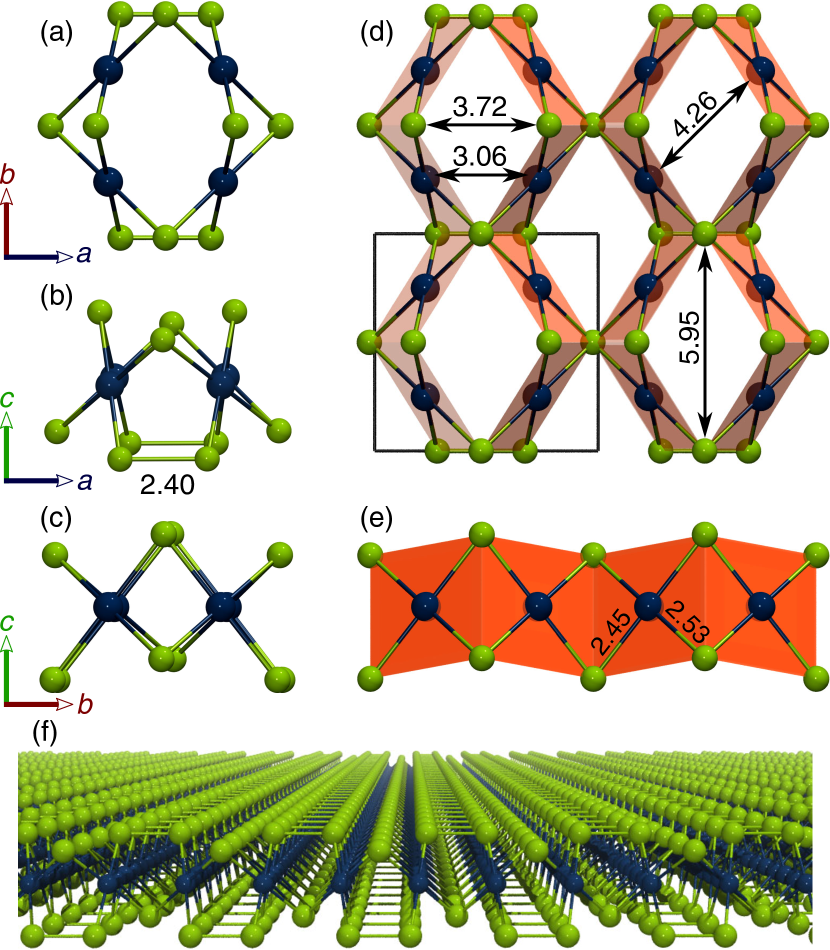
Experimentally, Pd2Se3 monolayers have been synthesized by interlayer fusion of two defective PdSe2 layers. 50 The monolayer is stable when exposed to air and at elevated temperatures 50. Its crystal structure has an inversion center with the point group of () and DFT calculated lattice parameters are 6.12 and 5.95 Å. As shown in Figure 1, the Pd atom has a square-planar coordination formed by [Se2]2- and Se2-. Such a coordination geometry is common among transition-metal complexes with the electronic configuration 12, 16, suggesting that the oxidation state of Pd is 2+ in Pd2Se3. Therefore, the coexistence of [Se2]2- dimers and Se2- anions leads to oxidation states of the stoichiometric compound as [Pd2+]2[Se]2-[Se2]2-. The formation of [Se2]2- dimers are supported by DFT calculated electron localization function (ELF) shown in Figure 4 (e), where the attractors (red area) on the midpoint of two selenide atoms indicate the covalent nature of bonding. The calculated Se–Se bond length of 2.4 Å (see Figure 1) is consistent with a fully oxidized two-center two-electron [Se2]2- dimer 62. Therefore, there are two types of Pd–Se bonds in the Pd2Se3 monolayer: the longer Pd–Se bond formed between Pd2+ cation and Se2- anion (2.53 Å) and the shorter one formed between Pd2+ and dimer (2.45Å). The resulting crystal structure is thus complex with large rhombus-shape voids, as shown in Figure 1.
Slack’s theory 63 reveals that four factors lead to low : i) complex crystal structure, ii) high average mass, iii) weak interatomic bonding, and iv) anharmonicity. As will be discussed later, the complex crystal structure of Pd2Se3 features all those key characteristics, in particular, a strong anharmonicity stemming from the [Se2]2- dimer.
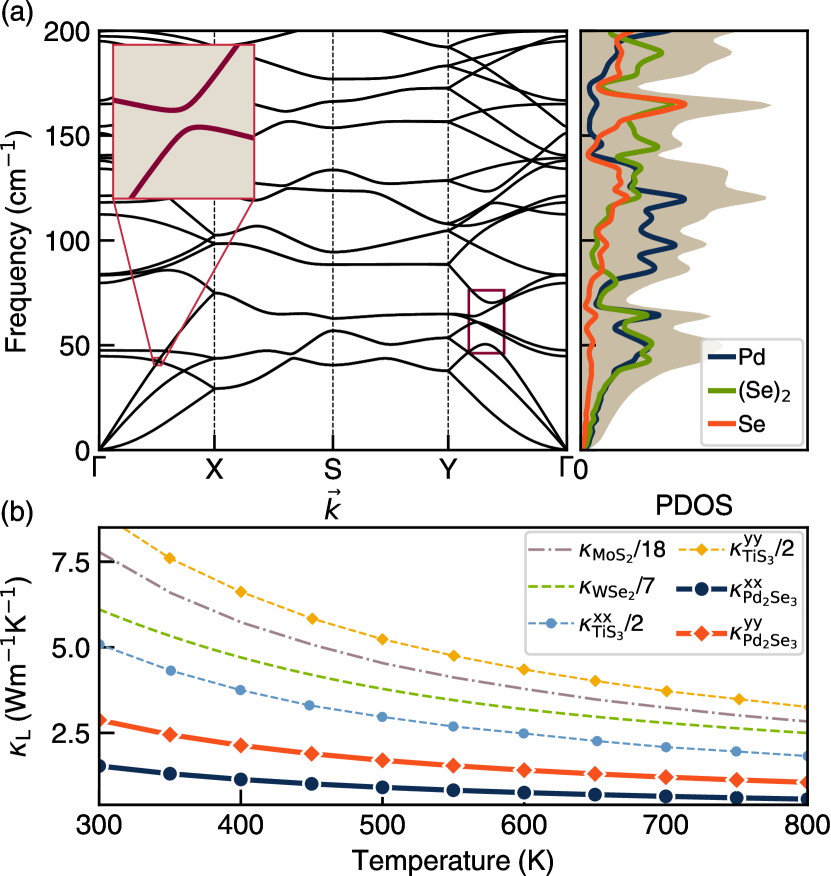
Figure 2 (a) displays the phonon dispersion of the Pd2Se3 monolayer. The frequencies of all modes are positive in the whole Brillouin zone (BZ), implying that the Pd2Se3 monolayers are dynamically stable.
The zone-boundary frequencies along – and - are as low as 30 and 40 cm-1. As seen in Figure 2, the acoustic bands, which play a dominant role in lattice heat transfer, have frequencies from 0 to 70 cm-1, and are mainly localized on [Se2]2- dimers and Pd2+ cations. Although Se2- is light and its associated vibrations appear at high-frequency regions, the [Se2]2- dimer acts like a heavy atom participating in low-frequency vibration modes.
The for each direction (i.e., - and -axes) is proportional to the square of the phonon group velocity along the respective direction65. The phonon group velocities of Pd2Se3 for the out-of-plane acoustic (ZA), transverse acoustic (TA), and longitudinal acoustic (LA) modes in the long-wavelength limit are listed in Table 1. The sound velocities of Pd2Se3 for all the acoustic branches are lower than those of MoS2 and TiS3 43, suggesting a lower in the Pd2Se3 monolayer. On the other hand, the avoided crossing between the optical and acoustic modes is clearly seen in Figure 2 (a) along –X and –Y directions. The sizable gap at the avoided crossing point indicates a high coupling strength (hybridization) between optical and acoustic modes, which significantly increases the phonon scattering rates and reduces acoustic mode velocities, and thus leads to the low .
For the quantitative description of , we use first-principles calculations in conjunction with the self-consistent iterative solution of the Boltzmann transport equation (BTE) for phonons as implemented in ShengBTE 58. The calculated as a function of temperature along the - and directions are shown in Figure 2 (b). The lattice thermal conductivity along the () and -axes () are 1.5 and 2.85 Wm-1K-1 at 300 K, respectively. They are comparable to those of high bulk materials such as PbTe, but much lower than other TMCs monolayers such as MoS2 (140 Wm-1K-1), TiSe3 (10 Wm-1K-1), and WSe2 (42 Wm-1K-1). The calculated cumulative with respect to mean free path is shown in Figure S7. The result indicates that the can be further reduced by decreasing grain size of the polycrystal; for instance, at the size of 75 nm the and of the Pd2Se3 monolayer drop by 50%.
| Monolayer | Direction | ZA (Km/s) | TA(Km/s) | LA(km/s) |
|---|---|---|---|---|
| Pd2Se3 | 0.51 | 2.25 | 3.12 | |
| 0.50 | 2.27 | 3.19 | ||
| TiS3 | 0.88 | 3.01 | 5.43 | |
| 1.11 | 2.31 | 6.16 | ||
| MoS2 | , | 1.40 | 3.96 | 6.47 |
A comparison of for two selenide based TMCs monolayers, Pd2Se3 and WSe2, is illuminating. The atomic mass of the Pd (106.42) is much smaller than the W (183.4) and thus one might expect a higher for the Pd2Se3. Nevertheless, as seen in Figure 2 the calculated of the Pd2Se3 monolayer is more than 20 times lower than WSe2. We next explore the origin of this behavior.
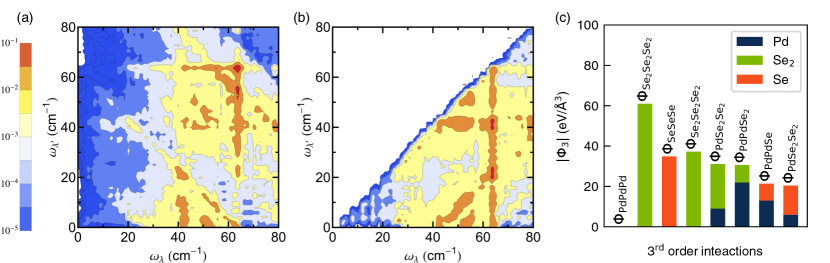
From the cumulative of phonon frequency (see Figure S8 in Supplementary Materials) we see that lattice heat transport is dominated by phonon modes with frequencies less than 80 cm-1. In Figure 3 (a) and (b) we show the scattering rates associated with these low-lying phonon modes from three-phonon interactions, namely, the absorption (: ) and emission (:) processes. Different colors in the scattering rates plot show the scattering magnitude of the first phonon mode () induced by the second phonon mode (). In the absorption process, a low-frequency phonon mode contributes to other low-frequency phonon modes, giving rise to a high-frequency optical mode. In the emission process, the phonon mode is only allowed to decompose into a lower-frequency mode, thus restricting the second phonon mode () in the right lower triangle. Both processes satisfy energy and crystal-momentum conservation. Figure 3 (a) shows the strong scattering of acoustic modes through combination with low-lying optical modes ( 40 cm-1), which is near the avoided crossing, consisting with high scattering rates due to avoided crossing bands. Phonon modes with frequencies ranging from 40 to 70 cm-2, as shown in Figure 3 (a) and (b), are heavily scattered in both absorption and emission processes, indicating that the presence of low-lying optical modes significantly enhances overall phonon scattering rates.
To specify the role of each atom in the observed low , we calculate the atom projected , as shown in Figure S9 in Supplementary Materials. [Se2]2- dimers and Pd2+ cation are largely responsible (90% in total) for heat transport in the Pd2Se3 monolayer, whereas the contribution of Se2- is negligible. We also calculate the norm of third-order IFCs defined as ( and are the total energy and atom displacement for different atom species , , and ). Since the phonon scattering rates are roughly proportional to 58, 66, a high absolute value of suggests a large anharmonicity. As shown in Figure 3 (c), indicates a large anharmonicity associated with [Se2]2- dimers, which is much higher than Pd2+ and Se2- anions. Therefore, the low is a combined effect of strong anharmonic phonon-phonon interactions and small group velocities, stemming from the formation of [Se2]2- dimers. This answers the question on why Pd2Se3 has a much lower than other TMCs, where such dimers do not form.
2 Electronic
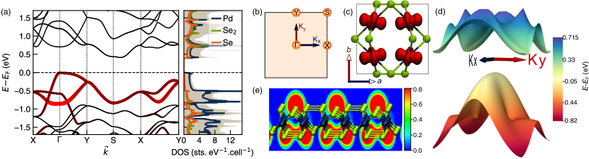
As already mentioned, in the Pd2Se3 monolayers the Pd2+ cation has a electronic configuration and a square planar crystal field, under which obritals split into four energy levels, /, , , and from low to high energy. On the other hand, the packing of square planar units in the crystal lattice induces a weak interaction between the nearby Pd2+ cations, separated by 3.06 Å, via obritals as seen in Figure 4 (c). This interaction switches the energy levels of with (see Figure S1 in Supplementary Materials). Note that in the Pd2Se3 monolayers, the orbital almost lies along the -axis. Due to the strong crystal field splitting associated with square planar geometry, the low spin state is always preferred in Pd2+. As a result, the four low-energy levels are occupied by the eight electrons of Pd2+ () cations, where the is the highest occupied orbitals (the top of the valence band). Therefore the Pd2Se3 monolayer is a band insulator, in which the top of the valence band is mainly composed of orbital, as seen in Figure 4 (a), and the bottom of the conduction band is largely from (see Figure S2).
As the overlap of orbital with the and orbitals of the nearest anion is negligible, a relatively flat band along the -axis is expected. As seen in Figure 4 (a) and (b), the valence band maximum along the is relatively flat, affording a high density of states (DOS) near the Fermi level. On the other hand, a proper overlap between Pd2+ orbitals along the -axis leads to a very dispersive band along the direction, indicating a small band effective mass and therefore high carrier mobility. This type of band structure, known as the flat-and-dispersive or “pudding-mold” type band structure, has been found in high-performance bulk TE materials16 such as NaxCoO2 14, 15, Bi2PdO4 12, and some full Heusler compounds.13, 67 This actually coincides with the idea proposed by Mahan and Sofo 66 that “we have to search for materials where the distribution of energy carriers is as narrow as possible, but with high carrier velocity in the direction of the applied electric field.”. A highly dispersive band (small band effective mass) around the Fermi level gives rise to a large , while a sharp increase in the density of states owing to the presence of a flat band (large band effective mass) usually leads to a large 66. In the case of the Pd2Se3 monolayers, the calculated effective masses () for holes along the dispersive band is about 0.17 m0 and for the flat band is 9.14 m0, thus a high and are expected along the -axis.
In Figure 5, we plot the calculated electronic transport coefficients for hole (-type) and electron (-type) doped Pd2Se3 monolayers at varying temperatures. The calculated PF along the -axis for both -type and -type systems, assuming s and T=300 K, are respectively 1.61 and 1.29 mW/mK2. Along the -axis, while the PF of -type is large (0.7 mW/mK2), the -type is quite small (0.1 mW/mK2). Thus, a large PF anisotropy is established with a dominant PF along the -axis in the -type Pd2Se3 monolayers. Using the same electronic relaxation time, the maximum PF for MoS2, MoSe2, WSe2, and TiS3 at the same temperature are 1.8 mW/mK2 (-type)68, 0.8 mW/mK2 (-type)28, 1.7 mW/mK2 (-type)28 and 1.8 mW/mK2 (-type) 43, respectively. The PF of Pd2Se3 monolayers, 1.61 mW/mK2 (-type) and 1.21 mW/mK2 (-type), is comparable to these TMCs, while its is one to two orders of magnitudes lower (see Figure 2). Therefore, a larger for the Pd2Se3 monolayers is expected.
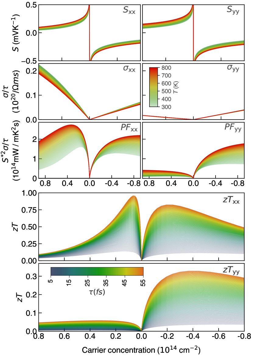
In Figure 5 we calculate the at the varying relaxation times within a reasonable range 69 from 5 to s. The of -type Pd2Se3 monolayers along the -axis is about 16% larger than the -type one. Depending on the relaxation time the calculated -type values vary between 0.15 to 1. Along -axis, a large difference between - and -type values is found. Using the same , our calculated values are much larger than the previously reported TMCs such as TiS3 43, MoSe2, WSe2 28, PtSe2 29. Our calculations suggest that Pd2Se3 monolayers are promising TE material in both -type and -type applications.
In conclusion, we investigated the electronic structure, phonon, and electron and phonon transport properties of the recently synthesized Pd2Se3 monolayers by the means of first-principles calculations and Boltzmann transport theory. Our results demonstrate that the Pd2Se3 monolayers possess a much lower lattice thermal conductivity than other TMC monolayers, e.g., MoS2, MoSe2, WSe2, Ti2Se3. Detailed analysis of third-order force constants indicates that the anharmonicity and soft phonon modes associated with [Se2]2- dimers are responsible for the low lattice thermal conductivity of Pd2Se3. On the other hand, the “pudding-mold” type band structure, originating from the square-planar coordinated Pd2+ cation, offers a high power factor. An extremely low lattice thermal conductivity in conjunction with a high power factor leads, of course, to the superior TE performance in the Pd2Se3 monolayer. Our results suggest the Pd2Se3 monolayer is a promising two-dimensional thermoelectric material with a high for both hole and electron doping.
ACKNOWLEDGMENTS
J. H. and C. W. (electronic structure, thermoelectric calculations and analysis) acknowledge support by the U.S. Department of Energy, Office of Science and Office of Basic Energy Sciences, under Award No. DE-SC0014520. Y.X (analysis of phonon calculations) acknowledges the Center for Nanoscale Materials, an Office of Science user facility, supported by the U. S. Department of Energy, Office of Science, Office of Basic Energy Sciences, under Contract No. DE-AC02-06CH11357. The authors acknowledge computing resources provided on Blues, a high-performance computing cluster operated by the Laboratory Computing Resource Center at Argonne National Laboratory.
References
- Rowe 1995 Rowe, D. M. CRC handbook of thermoelectrics; CRC press, 1995
- Kraemer et al. 2011 Kraemer, D.; Poudel, B.; Feng, H.-P.; Caylor, J. C.; Yu, B.; Yan, X.; Ma, Y.; Wang, X.; Wang, D.; Muto, A.; McEnaney, K.; Chiesa, M.; Ren, Z.; Chen, G. High-performance flat-panel solar thermoelectric generators with high thermal concentration. Nat Mater 2011, 10, 532–538
- Snyder and Toberer 2008 Snyder, G. J.; Toberer, E. S. Complex thermoelectric materials. Nat Mater 2008, 7, 105–114
- Toberer et al. 2011 Toberer, E. S.; Zevalkink, A.; Snyder, G. J. Phonon engineering through crystal chemistry. J. Mater. Chem. 2011, 21, 15843–15852
- Majumdar 2004 Majumdar, A. Thermoelectricity in Semiconductor Nanostructures. Science 2004, 303, 777–778
- Xie et al. 2012 Xie, W.; Weidenkaff, A.; Tang, X.; Zhang, Q.; Poon, J.; Tritt, T. Recent Advances in Nanostructured Thermoelectric Half-Heusler Compounds. Nanomaterials 2012, 2, 379–412
- Poudel et al. 2008 Poudel, B.; Hao, Q.; Ma, Y.; Lan, Y.; Minnich, A.; Yu, B.; Yan, X.; Wang, D.; Muto, A.; Vashaee, D.; Chen, X.; Liu, J.; Dresselhaus, M. S.; Chen, G.; Ren, Z. High-Thermoelectric Performance of Nanostructured Bismuth Antimony Telluride Bulk Alloys. Science 2008, 320, 634–638
- Biswas et al. 2012 Biswas, K.; He, J.; Blum, I. D.; Chun-IWu,; Hogan, T. P.; Seidman, D. N.; Dravid, V. P.; Kanatzidis, M. G. Corrigendum: High-performance bulk thermoelectrics with all-scale hierarchical architectures. Nature 2012, 490, 570–570
- Pei et al. 2011 Pei, Y.; Shi, X.; LaLonde, A.; Wang, H.; Chen, L.; Snyder, G. J. Convergence of electronic bands for high performance bulk thermoelectrics. Nature 2011, 473, 66–69
- Liu et al. 2012 Liu, W.; Tan, X.; Yin, K.; Liu, H.; Tang, X.; Shi, J.; Zhang, Q.; Uher, C. Convergence of Conduction Bands as a Means of Enhancing Thermoelectric Performance of -Type Solid Solutions. Phys. Rev. Lett. 2012, 108, 166601
- Yu et al. 2012 Yu, B.; Zebarjadi, M.; Wang, H.; Lukas, K.; Wang, H.; Wang, D.; Opeil, C.; Dresselhaus, M.; Chen, G.; Ren, Z. Enhancement of thermoelectric properties by modulation-doping in silicon germanium alloy nanocomposites. Nano Lett. 2012, 12, 2077–2082
- He et al. 2017 He, J.; Hao, S.; Xia, Y.; Naghavi, S. S.; Ozoliņš, V.; Wolverton, C. Bi2PdO4 : A Promising Thermoelectric Oxide with High Power Factor and Low Lattice Thermal Conductivity. Chem. Mater. 2017, 29, 2529–2534
- Bilc et al. 2015 Bilc, D. I.; Hautier, G.; Waroquiers, D.; Rignanese, G.-M.; Ghosez, P. Low-Dimensional Transport and Large Thermoelectric Power Factors in Bulk Semiconductors by Band Engineering of Highly Directional Electronic States. Phys. Rev. Lett. 2015, 114, 136601
- Usui and Kuroki 2017 Usui, H.; Kuroki, K. Enhanced power factor and reduced Lorenz number in the Wiedemann–Franz law due to pudding mold type band structures. Journal of Applied Physics 2017, 121, 165101
- Kuroki and Arita 2007 Kuroki, K.; Arita, R. “Pudding Mold” Band Drives Large Thermopower in NaxCoO2. J. Phys. Soc. Japan 2007, 76, 083707
- Isaacs and Wolverton 2018 Isaacs, E. B.; Wolverton, C. Inverse Band Structure Design via Materials Database Screening: Application to Square Planar Thermoelectrics. Chemistry of Materials 2018,
- Mateeva et al. 1998 Mateeva, N.; Niculescu, H.; Schlenoff, J.; Testardi, L. R. Correlation of Seebeck coefficient and electric conductivity in polyaniline and polypyrrole. J. Appl. Phys. 1998, 83, 3111–3117
- Hicks and Dresselhaus 1993 Hicks, L. D.; Dresselhaus, M. S. Thermoelectric figure of merit of a one-dimensional conductor. Phys. Rev. B 1993, 47, 16631–16634
- Dresselhaus et al. 1999 Dresselhaus, M. S.; Dresselhaus, G.; Sun, X.; Zhang, Z.; Cronin, S. B.; Koga, T. Low-dimensional thermoelectric materials. Phys. Solid State 1999, 41, 679–682
- Dresselhaus et al. 2007 Dresselhaus, M. S.; Chen, G.; Tang, M. Y.; Yang, R.; Lee, H.; Wang, D.; Ren, Z.; Fleurial, J.-P.; Gogna, P. New directions for low-dimensional thermoelectric materials. Advanced materials 2007, 19, 1043–1053
- Harman 2002 Harman, T. C. Quantum Dot Superlattice Thermoelectric Materials and Devices. Science 2002, 297, 2229–2232
- Venkatasubramanian et al. 2001 Venkatasubramanian, R.; Siivola, E.; Colpitts, T.; O’Quinn, B. Thin-film thermoelectric devices with high room-temperature figures of merit. Nature 2001, 413, 597–602
- Hochbaum et al. 2008 Hochbaum, A. I.; Chen, R.; Delgado, R. D.; Liang, W.; Garnett, E. C.; Najarian, M.; Majumdar, A.; Yang, P. Enhanced thermoelectric performance of rough silicon nanowires. Nature 2008, 451, 163–167
- Zhang et al. 2012 Zhang, G.; Kirk, B.; Jauregui, L. A.; Yang, H.; Xu, X.; Chen, Y. P.; Wu, Y. Rational Synthesis of Ultrathin n-Type Bi2Te3 Nanowires with Enhanced Thermoelectric Properties. Nano Lett. 2012, 12, 56–60
- Fei et al. 2014 Fei, R.; Faghaninia, A.; Soklaski, R.; Yan, J.-A.; Lo, C.; Yang, L. Enhanced Thermoelectric Efficiency via Orthogonal Electrical and Thermal Conductances in Phosphorene. Nano Lett. 2014, 14, 6393–6399
- Yang et al. 2014 Yang, K.; Cahangirov, S.; Cantarero, A.; Rubio, A.; D’Agosta, R. Thermoelectric properties of atomically thin silicene and germanene nanostructures. Phys. Rev. B 2014, 89, 125403
- Huang et al. 2013 Huang, W.; Da, H.; Liang, G. Thermoelectric performance of M ( Mo,W; S,Se) monolayers. J. Appl. Phys. 2013, 113, 104304
- Kumar and Schwingenschlögl 2015 Kumar, S.; Schwingenschlögl, U. Thermoelectric Response of Bulk and Monolayer MoSe2 and WSe2. Chem. Mater. 2015, 27, 1278–1284
- Guo 2016 Guo, S.-D. Biaxial strain tuned thermoelectric properties in monolayer PtSe2. J. Mater. Chem. C 2016, 4, 9366–9374
- Wu et al. 2014 Wu, J.; Schmidt, H.; Amara, K. K.; Xu, X.; Eda, G.; Özyilmaz, B. Large thermoelectricity via variable range hopping in chemical vapor deposition grown single-layer MoS2. Nano Lett. 2014, 14, 2730–2734
- Yoshida et al. 2016 Yoshida, M.; Iizuka, T.; Saito, Y.; Onga, M.; Suzuki, R.; Zhang, Y.; Iwasa, Y.; Shimizu, S. Gate-Optimized Thermoelectric Power Factor in Ultrathin WSe 2 Single Crystals. Nano Lett. 2016, 16, 2061–2065
- Buscema et al. 2013 Buscema, M.; Barkelid, M.; Zwiller, V.; van der Zant, H. S. J.; Steele, G. A.; Castellanos-Gomez, A. Large and Tunable Photothermoelectric Effect in Single-Layer MoS 2. Nano Lett. 2013, 13, 358–363
- Li et al. 2013 Li, W.; Carrete, J.; Mingo, N. Thermal conductivity and phonon linewidths of monolayer MoS 2 from first principles. Appl. Phys. Lett. 2013, 103, 253103
- Guo 2016 Guo, S.-D. Strain effect on power factor in monolayer Mo. Comput. Mater. Sci. 2016, 123, 8–13
- Ding et al. 2016 Ding, G.; Gao, G. Y.; Huang, Z.; Zhang, W.; Yao, K. Thermoelectric properties of monolayer MSe2 ( Zr, Hf): low lattice thermal conductivity and a promising figure of merit. Nanotechnology 2016, 27, 375703
- Guo and Wang 2017 Guo, S. D.; Wang, Y. H. Thermoelectric properties of orthorhombic group IV-VI monolayers from the first-principles calculations. J. Appl. Phys. 2017, 121, 034302
- Shafique and Shin 2017 Shafique, A.; Shin, Y.-H. Thermoelectric and phonon transport properties of two-dimensional compounds. Sci. Rep. 2017, 7, 506
- Jin et al. 2016 Jin, Z.; Liao, Q.; Fang, H.; Liu, Z.; Liu, W.; Ding, Z.; Luo, T.; Yang, N. A Revisit to High Thermoelectric Performance of Single-layer MoS2. Sci. Rep. 2016, 5, 18342
- Sun et al. 2015 Sun, J.; Shi, H.; Siegrist, T.; Singh, D. J. Electronic, transport, and optical properties of bulk and mono-layer PdSe2. Appl. Phys. Lett. 2015, 107, 2–6
- Wang et al. 2017 Wang, J.; Xie, F.; Cao, X.-H.; An, S.-C.; Zhou, W.-X.; Tang, L.-M.; Chen, K.-Q. Excellent Thermoelectric Properties in monolayer WSe2 Nanoribbons due to Ultralow Phonon Thermal Conductivity. Sci. Rep. 2017, 7, 41418
- Wang et al. 2015 Wang, Y.; Li, Y.; Chen, Z. Not your familiar two dimensional transition metal disulfide: structural and electronic properties of the PdS2 monolayer. J. Mater. Chem. C 2015, 3, 9603–9608
- Zhang et al. 2016 Zhang, Z.; Xie, Y.; Peng, Q.; Chen, Y. A theoretical prediction of super high-performance thermoelectric materials based on MoS2/WS2 hybrid nanoribbons. Sci. Rep. 2016, 6, 21639
- Zhang et al. 2017 Zhang, J.; Liu, X.; Wen, Y.; Shi, L.; Chen, R.; Liu, H.; Shan, B. Titanium Trisulfide Monolayer as a Potential Thermoelectric Material: A First-Principles-Based Boltzmann Transport Study. ACS Appl. Mater. Interfaces 2017, 9, 2509–2515
- Peng et al. 2016 Peng, B.; Zhang, H.; Shao, H.; Xu, Y.; Zhang, X.; Zhu, H. Thermal conductivity of monolayer MoS2, MoSe2, and WS2: interplay of mass effect, interatomic bonding and anharmonicity. RSC Adv. 2016, 6, 5767–5773
- Chhowalla et al. 2013 Chhowalla, M.; Shin, H. S.; Eda, G.; Li, L.-J.; Loh, K. P.; Zhang, H. The chemistry of two-dimensional layered transition metal dichalcogenide nanosheets. Nat. Chem. 2013, 5, 263–275
- Yun et al. 2012 Yun, W. S.; Han, S. W.; Hong, S. C.; Kim, I. G.; Lee, J. D. Thickness and strain effects on electronic structures of transition metal dichalcogenides: 2H- semiconductors ( Mo, W; S, Se, Te). Phys. Rev. B 2012, 85, 033305
- Island et al. 2014 Island, J. O.; Buscema, M.; Barawi, M.; Clamagirand, J. M.; Ares, J. R.; Sánchez, C.; Ferrer, I. J.; Steele, G. A.; van der Zant, H. S.; Castellanos-Gomez, A. Ultrahigh photoresponse of few-layer TiS3 nanoribbon transistors. Adv. Opt. Mater. 2014, 2, 641–645
- Lipatov et al. 2015 Lipatov, A.; Wilson, P.; Shekhirev, M.; Teeter, J.; Netusil, R.; Sinitskii, A. Few-layered titanium trisulfide (TiS<inf>3</inf>) field-effect transistors. Nanoscale 2015, 7, 12291–12296
- Pawbake et al. 2015 Pawbake, A. S.; Island, J. O.; Flores, E.; Ares, J. R.; Sanchez, C.; Ferrer, I. J.; Jadkar, S. R.; Van Der Zant, H. S.; Castellanos-Gomez, A.; Late, D. J. Temperature-Dependent Raman Spectroscopy of Titanium Trisulfide (TiS3) Nanoribbons and Nanosheets. ACS Appl. Mater. Interfaces 2015, 7, 24185–24190
- Lin et al. 2017 Lin, J.; Zuluaga, S.; Yu, P.; Liu, Z.; Pantelides, S. T.; Suenaga, K. Novel Pd2Se3 Two-Dimensional Phase Driven by Interlayer Fusion in Layered PdSe2. Phys. Rev. Lett. 2017, 119, 016101
- Allen 1996 Allen, P. Boltzmann theory and resistivity of metals. KLUWER INTERNATIONAL SERIES IN ENGINEERING AND COMPUTER SCIENCE 1996, 219–250
- Blöchl 1994 Blöchl, P. E. Projector augmented-wave method. Phys. Rev. B 1994, 50, 17953–17979
- Kresse and Joubert 1999 Kresse, G.; Joubert, D. From ultrasoft pseudopotentials to the projector augmented-wave method. Phys. Rev. B 1999, 59, 1758–1775
- Kresse and Furthmüller 1996 Kresse, G.; Furthmüller, J. Efficient iterative schemes for ab-initio total-energy calculations using a plane-wave basis set. Phys. Rev. B 1996, 54, 11169–11186
- Kresse and Furthmüller 1996 Kresse, G.; Furthmüller, J. Efficiency of ab-initio total energy calculations for metals and semiconductors using a plane-wave basis set. Comput. Mater. Sci. 1996, 6, 15–50
- Perdew et al. 1997 Perdew, J. P.; Burke, K.; Ernzerhof, M. Generalized Gradient Approximation Made Simple. Phys. Rev. Lett. 1997, 78, 1396–1399
- Madsen and Singh 2006 Madsen, G. K.; Singh, D. J. BoltzTraP. A code for calculating band-structure dependent quantities. Computer Physics Communications 2006, 175, 67 – 71
- Li et al. 2014 Li, W.; Carrete, J.; Katcho, N. A.; Mingo, N. ShengBTE: a solver of the Boltzmann transport equation for phonons. Comp. Phys. Commun. 2014, 185, 1747–1758
- Li et al. 2012 Li, W.; Mingo, N.; Lindsay, L.; Broido, D. A.; Stewart, D. A.; Katcho, N. A. Thermal conductivity of diamond nanowires from first principles. Phys. Rev. B 2012, 85, 195436
- Li et al. 2012 Li, W.; Lindsay, L.; Broido, D. A.; Stewart, D. A.; Mingo, N. Thermal conductivity of bulk and nanowire Mg2SixSn1-x alloys from first principles. Phys. Rev. B 2012, 86, 174307
- Togo et al. 2008 Togo, A.; Oba, F.; Tanaka, I. First-principles calculations of the ferroelastic transition between rutile-type and -type at high pressures. Phys. Rev. B 2008, 78, 134106
- O’Keeffe and Brese 1992 O’Keeffe, M.; Brese, N. E. Bond-valence parameters for anion-anion bonds in solids. Acta Crystallogr. Sect. B Struct. Sci. 1992, 48, 152–154
- Slack 1973 Slack, G. Nonmetallic crystals with high thermal conductivity. J. Phys. Chem. Solids 1973, 34, 321–335
- Gandi and Schwingenschlögl 2016 Gandi, A. N.; Schwingenschlögl, U. Thermal conductivity of bulk and monolayer MoS 2. EPL (Europhysics Lett. 2016, 113, 36002
- Mingo et al. 2014 Mingo, N.; Stewart, D.; Broido, D.; Lindsay, L.; Li, W. Length-Scale Dependent Phonon Interactions; Springer, 2014; pp 137–173
- Mahan and Sofo 1996 Mahan, G. D.; Sofo, J. O. The best thermoelectric. Proc. Natl. Acad. Sci. 1996, 93, 7436–7439
- He et al. 2016 He, J.; Amsler, M.; Xia, Y.; Naghavi, S. S.; Hegde, V. I.; Hao, S.; Goedecker, S.; Ozoliņš, V.; Wolverton, C. Ultralow thermal conductivity in full Heusler semiconductors. Physical review letters 2016, 117, 046602
- Babaei et al. 2014 Babaei, H.; Khodadadi, J. M.; Sinha, S. Large theoretical thermoelectric power factor of suspended single-layer MoS 2. Appl. Phys. Lett. 2014, 105, 193901
- González-Romero et al. 2017 González-Romero, R. L.; Antonelli, A.; Meléndez, J. J. Insights into the thermoelectric properties of SnSe from ab initio calculations. Phys. Chem. Chem. Phys. 2017, 19, 12804–12815